1. Introduction
Silicon, as the most common semiconductor in electronic integrated circuits, has been considered as one of the best candidates for the natural hybrid of photonic and electronic devices [
1]. In recent years, various silicon-based devices have been proposed for the generation, modulation and detection of light [
2,
3,
4,
5]. The combination of silicon photonics with electronic devices not only brings the advantage of improved bandwidth and fundamental speed, but also shows the potential of massive production with low fabrication cost in comparison with other semiconductors. Among all the silicon-based photonics units, the optical modulator, as one of the most critical components in optical communication, thermal sensing and imaging systems, has drawn great research interest lately [
6].
The conventional approach to optical modulation is based on the first order electro-optical effect (Pockels effect) of materials. That is, by applying an external electric field, the dielectric function of the material alters and results in a modification of the optical response and a change of the reflectance or transmittance. However, as a centrosymmetric semiconductor, intrinsic silicon has a weak electro-optical coefficient and therefore is not an ideal material for implementation in electro-optical modulation [
7,
8]. As an alternative method, thermal-optical modulation was investigated by Cocorullo et al., but it is only suitable for low repetition rate applications due to its slow response [
9,
10]. Currently, the free carrier plasma dispersion effect, where the material optical response varied with the free carrier density, is the most commonly-investigated modulation mechanism in silicon [
11]. The free carrier density can be altered by the carrier depletion, accumulation or injection by either electronic or optical means [
12]. The latter case is known as all-optical modulation, which has its primary advantage in ultrafast modulation speed, typically in the picosecond range [
13]. As early as in 2004, Almeida et al. demonstrated a scheme of ultrafast all-optical modulation with silicon photonic structures in telecommunication wavelengths. A modulation depth of
with less than a 500-ps modulation speed was achieved [
14]. Soon after, Takasumi’s team reported an improved modulation speed of 70 ps by using ion-implanted silicon photonic crystal nanocavities [
15]. So far, most of the research interests and achievements in silicon optical modulators (including the examples mentioned above) have explored the range of telecommunication wavelengths. The Mid- to Long Wavelength Infrared region (MWIR and LWIR, respectively) has so far attracted less attention, despite the enormous potential and high demand on the market [
16].
The most demanding applications operating in MWIR, such as thermal imaging, security countermeasures and free space communication, exploit the high transmittance of the Earth’s atmosphere in the wavelength range between 3.5 and 5
m. A longer wavelength assures that there is less scattering compared to the near-infrared and visible light, as well as no active vibrational transitions of H
O and CO
molecules, making it suitable for remote sensing and detection with little influence from weather conditions [
17]. Despite the importance and maturity of the current MWIR detection and imaging technology, the present applications rely entirely on electronic and mechanical modulators, which limits the modulation speed to a few hundreds of nanoseconds. The development of all-optical modulators aims not only at improving the performance speed, but also at enabling new functionalities, such as ultrafast time-of-flight detection, anti-fluctuation atmosphere imaging and broadband free space communication, based on the current MWIR detection technologies [
18]. In 2011, Nedeljkovic et al. theoretically demonstrated the feasibility of all-optical modulation with crystalline silicon in a broad infrared range (1–14
m) [
19]. More recently, Shen et al. showed a 50-MHz all-optical modulator with germanium-on-silicon waveguides in the wavelength range between 2 and 3
m [
20]. In our previous work [
6], we used a time of flight detection scheme based on the all-optical modulation in the range between 2.1 and 3.5
m, demonstrating a potential to reach sub-picosecond temporal resolution. Up to date, there have been only a few experiments conducted on MWIR all-optical modulators, and the reported results only covered the short wavelength part of the mid-infrared spectrum.
In this work, we aim to explore for the first time a reflective-type silicon-based all-optical modulator in the wavelength range between 4 and 6 m, covering almost the entire MWIR range. Sub-wavelength structured silicon optical membranes were used as the active material for the modulator, and its reflectance in the MWIR regime was modified by external excitation of the free charge carriers (electron-hole plasma) using an intense laser beam of 800 nm. We show the overall performance of the modulator in the frequency and time domains and quantify the pump fluence required to achieve the optimised modulation. The results suggest the enhanced modulation depth of the sub-wavelength structured silicon in comparison to the bulk counterpart under the same experimental condition. An optical model was developed to fit the experimental data and extract the associated carrier concentration, charge carriers’ scattering rate and the complex dielectric function of the optically-excited membranes. We explored the temporal response of the modulator and designed the experimental conditions to achieve the ultrafast modulation of 0.55 ps. These unique conditions for the ultrafast switching in the time domain take advantage of the dielectric function variation following the carrier concentration evolution before reaching the equilibrium state and before the onset of the carrier density decay.
3. Optical Model
Before we proceed to the discussion of the results and analysis, we present the optical model, which aims to approximate the optical response and the experimentally-measured reflectance of the membranes. The main points that should be included in the model are: (1) approximation of the membrane dielectric function by the Maxwell–Garnett mixing rule; (2) incorporation of the contribution of the optically-excited free charge carriers into the dielectric function using the high-frequency conductivity Drude theory; (3) accounting for the variation of charge carrier density along the sample depth by Wentzel–Kramers–Brillouin (WKB) approximation.
The reflectance of a single-layer thin slab based on the WKB approximation is given by:
with the reflection coefficients of the front
and rear
interfaces, respectively. The
z-coordinate was chosen to be along the membrane depth.
and
q are
z-components of the wavevector of light outside and inside the material, respectively.
is the complex phase accumulated by the signal propagating through the sample with the thickness
m.
is the position-dependent wavevector of the signal along the sample depth, while
is the
x-component oriented parallel to the interfaces and has the same value of
outside of the material and at any location inside it; here,
is the angle of incidence. It can be seen that the model relies on the knowledge of the wavevector
, which is needed for the calculation of the phase,
, and the reflection coefficients
and
. To find
, one needs a good approximation of the effective dielectric function,
. The membrane structure has to be taken into account and the contribution of the free carriers excited by the pump should be considered. The later is, in general, non-uniform along the slab depth, but it can be approximated by
, where
F,
and
are the fluence, absorption coefficient and photon frequency of the pump. The dielectric function,
, which includes both contributions, the structures of the membrane and non-uniform longitudinal carrier distribution, can be calculated as follows:
where
is the intrinsic dielectric function of the bulk silicon,
is the volume fraction of the air pores,
and
are the optical mass and the scattering rate of the free carriers, and
is the frequency of the probe signal. In Equation (
2), the second term represents the 2D Maxwell–Garnett mixing rule, while the third term stands for the Drude contribution of the free carriers. The model and the fitting procedure were presented in more detail in previous publications on nanoporous silicon [
24,
25,
26,
27].
4. Wavelength Dependence and Ultrafast Temporal Response of Optically-Pumped Membranes
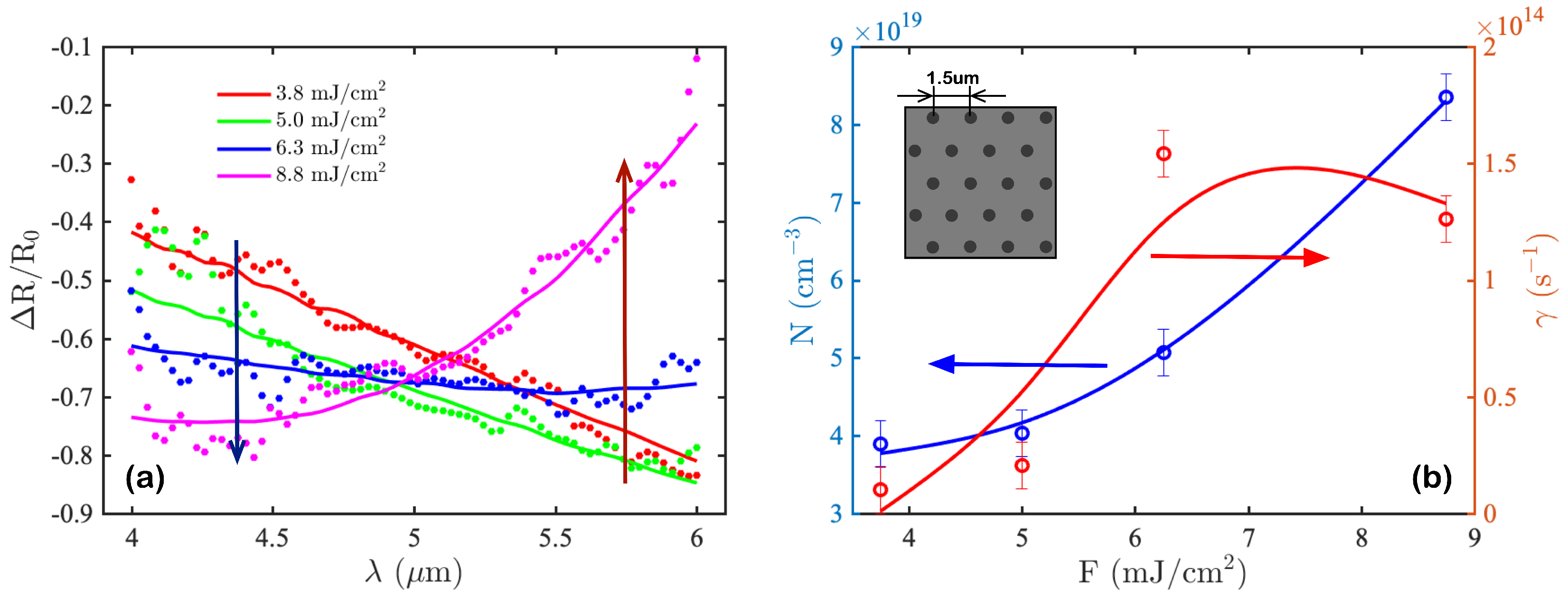
Figure 1a shows the reflectance change, ΔR/R
(R
R
)/R
, measured at the temporal overlap between the pump and signal pulses, as a function of the signal wavelength and for the different fluences of the pump, spanning between 3.8 and 8.8 mJ/cm
. R
and R
denote the reflectance with and without application of the pump pulse, respectively.
Figure 1a presents the experimental results as the dots and the model fitting, described in the previous section, as the solid lines. The corresponding carrier concentration used in the calculation of the optical model,
N, and scattering parameter,
, as a function of the pump fluence are shown in
Figure 1b. Note that
N and
are functions of the fluence only and were not influenced by the probe, as its fluence was too weak and the photon energy too small to alter them. In general, it can be seen that the optical model can be adequately fitted to the experimental results, providing a background to discuss the physics behind the findings and the feasibility to use the membranes for a reflective-type light modulator.
It can be seen that at certain conditions, the modulation efficiency can reach beyond 80%, yet it is not uniform over the entire range of wavelengths. At the lower fluence of about 4 mJ/cm
, the greatest modulation was observed at the longer wavelength of the spectrum around 6
m, while at the highest fluence, the situation was reversed: it was the shorter wavelength around 4
m that was the most affected. Such dependence of the reflectance spectra on the pump fluence can be considered for use in tunable spectral filters. At the lower pumping, the membrane acted as a shortwave reflecting filter, i.e., at 3.8 mJ/cm
, almost 70% of the 4
m probe was reflected back, while for 6
m, it was only 15%. At the highest fluence, the filter reflectance as a function of the wavelength was flipped over: it behaved as a a long-wavelength reflective filter with 90% of 6
m and 25% of 4
m reflected back, respectively. Overall, there are two critical details that need to be explained, which are the sign of the reflectance change as a function of the fluence, F, for a given wavelength
,
, indicated by the arrows on
Figure 1a, and its absolute value characterising the modulation contrast. It can be seen that
has the opposite sign: it was negative for the shorter wavelength and reversed to the opposite for the longer wavelength, while its absolute value was greater.
To understand this behaviour, one should examine Equation (
2) in terms of the evolution of
as a function of the injected free carrier density,
N, and relate it to the reflectance. When the carrier density,
N, increased, the dielectric function,
, monotonically dropped, yet the reflectance behaviour was more complex than that. At the lower carrier injection, when the third term in Equation (
2) was smaller than the sum of the first two, the increase of
N led to the decrease of the reflectance, while at a certain point where
, the minimum was reached, and the reflectance started to increase, reaching the maximum at
. The change of the sign at
corresponds to the onset of the transition of the optical response from dielectric to metal, also known as the plasma edge. Furthermore, it can be shown that in semiconductors at the conditions around the plasma edge for a given signal wavelength,
, the absolute value of reflectance change as a function of the carrier concentration has the relation of
. This discussion equally applies to
, assuming that
N is directionally proportional to
F. Thus, the opposite sign and the difference of the absolute values of the arrows in
Figure 1a indicated that the system was pumped in the region of dielectric-metal transition, where at the shorter wavelength
, while at longer wavelength approaching 6
m
and at the crossover around 5
m
. We note that, compared to the bulk semiconductor, less pumping was required to achieve this transition with structured membranes, as their dielectric function was lower due to the second negative term in Equation (
2), related to the dilution of
by the holes.
Figure 1b shows the fitting parameters used to calculate
. To improve the accuracy, we used a calculation routine that iteratively determines the real and imaginary parts of the effective dielectric function,
, in Equation (
2) from the amplitude and slope of the experimentally measured
as a function of
[
24]. The fitting results suggested that with the carrier concentration above 8 ×
cm
and scattering rate of about 1.5 ×
s
, dielectric-metal transition occurred for signals with
m. Moreover, it can be seen that
N is a non-linear function of
F; therefore, we had to correct our initial assumption of the linear absorption of the pump pulse. We note that a non-linear absorption in silicon optical membranes is not well-understood and reported, and we leave this point out of the arguments of this work. In addition, the scattering parameter,
, seemed to saturate at the higher fluences. We did not investigate this observation at a greater depth; however, the most likely reason for this is the saturation of the carrier-carrier collisions at the non-equilibrium conditions [
28].
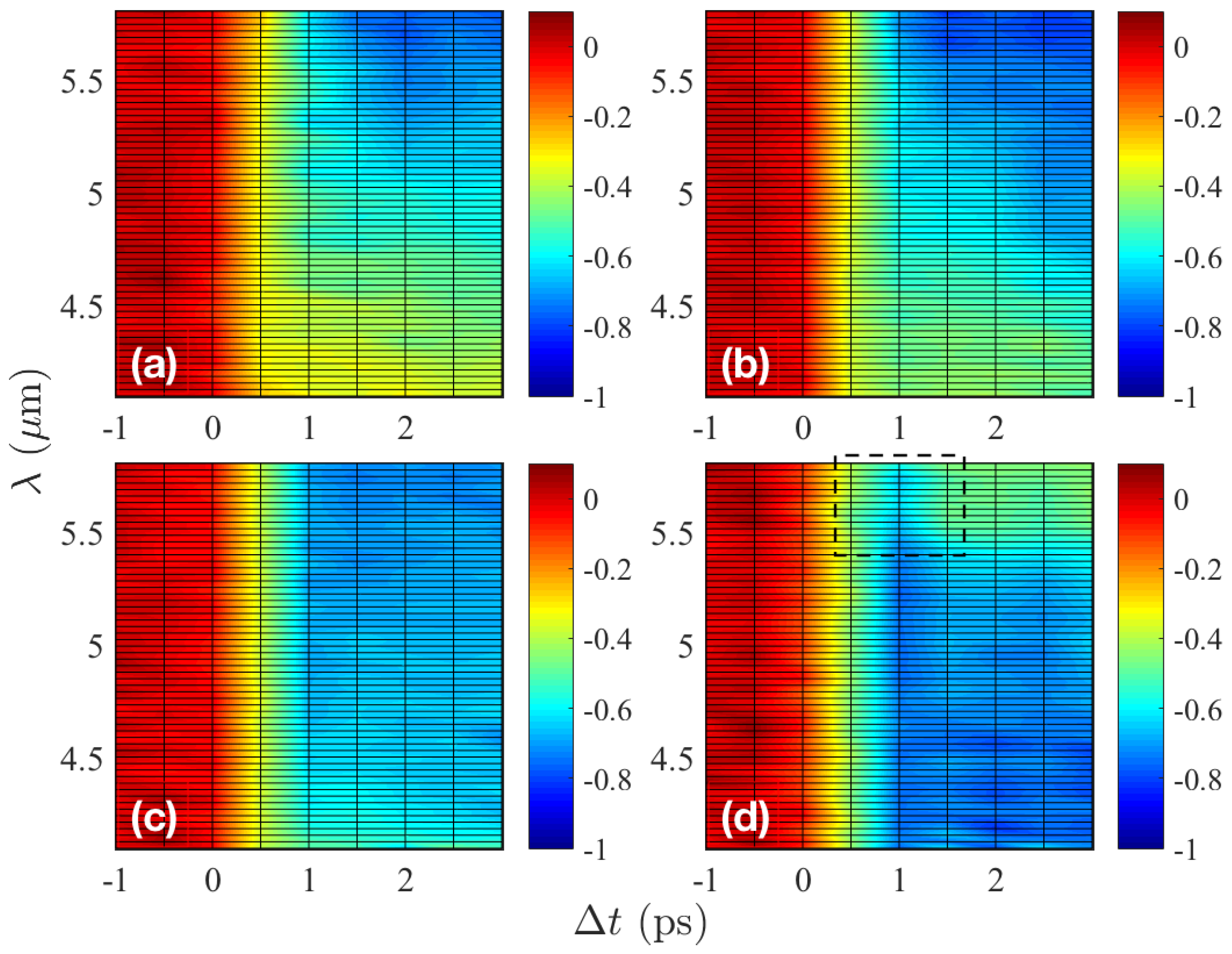
To further investigate the optical response and the temporal evolution of the spectra at different pump fluences, we performed ultrafast pump-probe measurements over a few picoseconds’ delay time between the pump and probe pulses. During this time, the injection of the charge carries reached saturation as the excitation process had been completed, but the recombination had not developed yet to affect the carrier density and optical response. We note that the temporal resolution was degraded by the convolution of the ultrafast excitation and somewhat longer probe pulse. The results are shown in
Figure 2a–d for the pump fluences of 3.8, 5.0, 6.3 and 8.8 mJ/cm
, respectively. These measurements can be viewed as the evolution of the curves shown in
Figure 1a as a function of time (along the horizontal axis).
Figure 2a–c show that after the excitation completed, the spectra did not change significantly after 1 ps as a function of the delay time,
. That is, once the equilibrium was achieved, the optical properties remained stable. However, in
Figure 2d, we observe a peculiar feature around 6
m and the delay time of 1 ps, as indicated by the dashed rectangular. Unlike anywhere else, in this region, the signal passed through the minimum before it recovered and stabilised. This curious behaviour was interesting for both understanding the physics behind the process and the possible development of applications. Indeed, such an ultrafast drop and recovery of the reflectance signal at a particular wavelength can be used for the extremely fast reflective-type all-optical switching. In the next section, we will focus on this ultrafast temporal variation of the reflected signal and discuss the physics behind it in more detail.
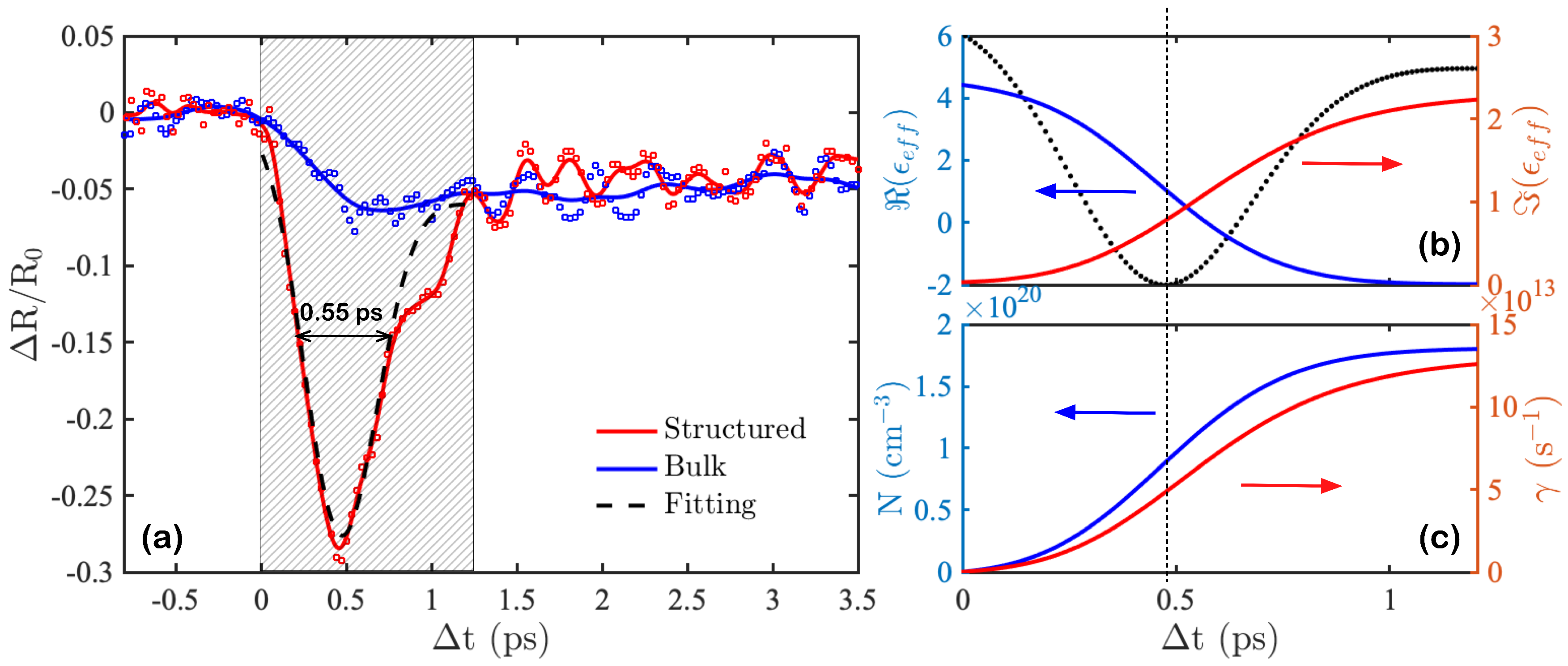
5. Demonstration of the Ultrafast Switching
Using the optical model shown above, we optimised the condition for the demonstration of the ultrafast switching, which can be operated at a speed far faster than the natural or enhanced decay processes in semiconductors related to trap states, surface recombination and Auger decay [
26,
29,
30,
31,
32,
33]. As an example of such a design, we show the reflective modulation of the signal at 4
m. This wavelength was also chosen because of its importance for the imaging and range-finding at MWIR [
6].
The performance of the modulator, demonstrating the contrast reaching 30% and the response time (as defined by the FWHM) of 0.55 ps, is shown in
Figure 3a. It surpassed an electro-optical reflective modulator based on a non-linear response of the surface plasmons [
34]. We noted that small oscillations of
for
ps were due the experimental noise and cannot be routinely reproduced.
Figure 3b shows the related temporal development of the real and complex parts of the effective dielectric function,
and
, following the excitation by the pump pulse. Besides, in
Figure 3c, we show the density of the carriers,
N, and their scattering rate,
, which transpired from the simulation of the experimentally-determined temporal evolution of
. The simulation itself is shown in
Figure 3a as the black dashed line.
We measured the bulk silicon to compare its performance with that of the optical membrane. In the absence of the pumping, the optical membranes and bulk silicon had reflectances of 0.2 and 0.3, respectively. It was apparent that for identical optical pumping, the response of the bulk silicon and optical membrane was quite different. The bulk material did not show a sharp negative peak, but rather dropped and remained constant. In addition, the modulation contrast was just above 5%.
To explain the sharp peaked response and enhancement in the modulation contrast, it will be helpful to investigate the development of
,
,
N and
as a function of time shown in
Figure 3b,c; Panel (b) also reproduces the reflectance response
as the dashed line for the convenience of the discussion. It can be seen that following the pump pulse application, the carrier density increased, causing a decrease of
and, alternatively, an increase of
. Yet at the earlier times, the main contribution to the reflectance change was from the variation of
, as
was still too small. Around 0.5 ps,
, at which
reached the minimum, and its value was set by
at this time. That is, higher
resulted in lower contrast of
. After 0.5 ps, the rate of
and its sign were determined by the the combined contribution of
and
as they have comparable absolute values. The steady state condition of
was reached after 1 ps when both the real and imaginary parts were saturated, on par with
N and
.
To summarise, initially, the rate of
drop was almost exclusively governed by the decrease of
; the minima was achieved when
; and the modulation contrast was determined by
. The
recovery rate was determined by the combination of the development of both
and
as a function of time, and their values determined the level at which
would saturate. We noted that the carriers did not recombine during this short time period, and therefore, the modulator switching speed did not depend on the recombination process. However, the modulator operation/repetition frequency was limited by the recombination time required for the modulator to return to the unexcited state before the next switching event happened. In our previous work, we showed that the complete recombination of the excited carriers occurred on the nanosecond time scale [
35].


