Article

An Inverter Topology for Wireless Power Transfer System with Multiple Transmitter Coils

by
Supapong Nutwong
,
Anawach Sangswang
* and
Sumate Naetiladdanon
Department of Electrical Engineering, Faculty of Engineering, King Mongkut’s University of Technology Thonburi, Bangkok 10140, Thailand
*
Author to whom correspondence should be addressed.
Appl. Sci. 2019, 9(8), 1551; https://doi.org/10.3390/app9081551
Submission received: 7 March 2019 / Revised: 27 March 2019 / Accepted: 11 April 2019 / Published: 14 April 2019
(This article belongs to the Section Electrical, Electronics and Communications Engineering)

Abstract

:
This paper presents an inverter topology for a wireless power transfer (WPT) system that is intended to reduce the component counts and complexity of the conventional excitation circuit for multiple transmitter coils. The proposed inverter topology requires only (n+2) power switches, where “n” is the number of transmitter coils. An excitation of a proper transmitter coil pattern with regard to the receiver coil position is determined. The output voltage can be regulated through the primary-side control by adjusting the duty cycles of the inverter switches. A detection method of the receiver coil position is presented using the detection switches on the secondary side. The detection algorithm is based on the reflected impedance knowledge and requires only a current sensor on the primary side. A proper transmitter coil pattern is energized to ensure maximum transfer efficiency throughout the operation. The proposed system is experimentally validated on the created 500-watt WPT multi-coil system. After the receiver coil is placed in a designated area, the proper transmitter coil pattern can be automatically selected and energized. The output voltage can be regulated to a desired value under the typical operation conditions, including load change.

1. Introduction

Safety, convenience, reliability, weatherproof, and maintenance-free are the key advantages of wireless power transfer (WPT) compared with wired or conductive power transfer [1]. Nowadays, the WPT technique has been successfully adopted in many applications, such as biomedical implants [2], electronic devices [3], kitchen appliances [4], electric vehicles [5], etc. A two-coil system, i.e., a single transmitter coil and a single receiver coil, is commonly found in conventional WPT systems. Both coils usually have the same shape and dimension, which simplifies the design and implementation [6,7]. The desired or ideal operation of the WPT system is that the receiver coil is always placed at the aligned position, where both the transmitter and receiver coils share the same center. The magnetic coupling coefficient is generally maximized at this position. Unfortunately, the misalignment between coupled coils is inevitable in practical operation. This leads to the magnetic coupling variation, which causes the output voltage or power to fluctuate. Moreover, the power transfer efficiency is drastically deteriorated with the reduction of the magnetic coupling coefficient [8,9,10]. Although the control of the duty cycle [11,12] or switching frequency [13,14] of the converter’s switches has been reported to address these problems, the misalignment tolerance is still limited to a low value. To improve the sensitivity to magnetic coupling variation, developments related to the coupled coil [15,16,17], optimized design of the magnetic core [18], and new compensation topology [19,20] are introduced. However, the transfer efficiency becomes problematic, because the magnetic coupling coefficient is reduced as the distance between coupled coils increases.
Recently, WPT multi-coil systems have become increasingly popular, especially in applications with free-positioning features. The key advantages of the multi-coil system include improvements in the working area and system efficiency compared with conventional two-coil systems [21,22,23]. However, excitation circuits for multiple transmitter coils remain an issue in the multi-coil system. A straightforward approach to a multi-coil configuration is to adopt multiple sources, where each transmitter coil is energized by an inverter. This increases component counts, cost, and size to the system. To achieve an optimal operation, there is a need for current regulation on each transmitter coil [24,25,26]. This often yields complicated control methods. The transmitter coils to be energized must be carefully selected, as the position of the receiver coil may be varied during operation. Energizing transmitter coils with weak coupling to the receiver coil would result in little to no contribution to the power transfer, and the system efficiency is sacrificed. A proper transmitter coil, where magnetic coupling is maximized, should be determined before the chosen transmitter coil pattern is energized. Therefore, the detection of the coil’s position and misalignment between coupled coils are indispensable. Pressure sensors [27], sensing coils [28], and tunneling magnetoresistive (TMR) sensors [29] have been adopted in past work. A tradeoff is that additional components and control are required, not to mention extra signal conditioner circuits to accommodate the sensors.
To reduce the component counts and complexity of the conventional excitation circuit for multiple transmitter coils, this paper presents a topology of the inverter circuit with receiver coil position detection. Only single-source and (n+2) power switches for n transmitter coils are required. The proposed inverter circuit can supply the transmitter coils individually or collectively, depending on the determined coil pattern. Each transmitter coil current flows in the same direction to produce a magnetic field with the same polarity. The DC output voltage is regulated through the primary-side control by adjusting the angle α of the inverter voltage. The detection method of the receiver coil position is introduced using detection switches on the secondary side. This method requires only a current sensor on the primary side. The proper transmitter coil pattern can be determined and energized by the proposed method. This improves the transfer efficiency of the WPT multi-coil system. This paper is organized as follows. The circuit configuration, timing diagram, and operating mode of the proposed system are described in Section 2. The detection method of the receiver coil position and selection of the transmitter coil pattern are proposed in Section 3. The proposed controller is outlined in Section 4. Experimental validation of the proposed system is presented in Section 5. Section 6 concludes this work.

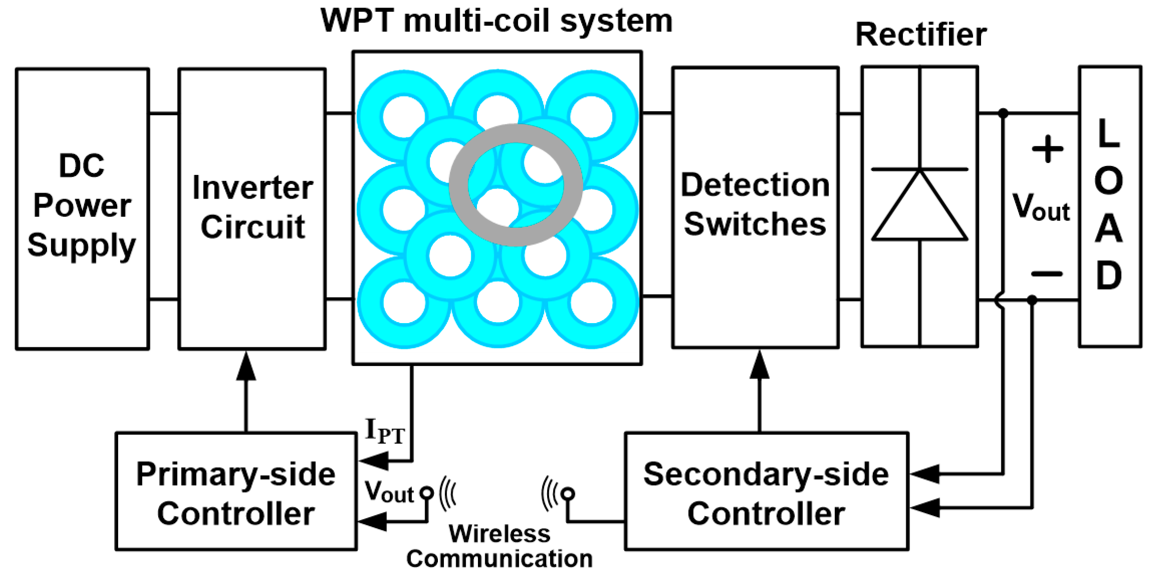
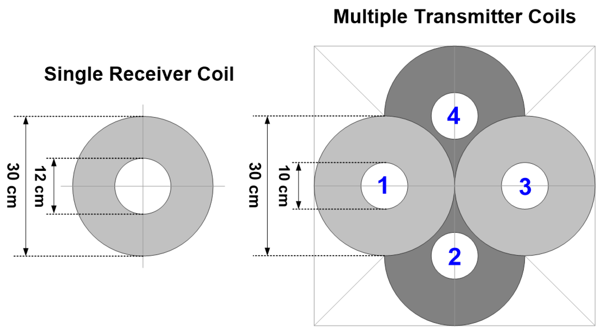
2. System Description and Operation

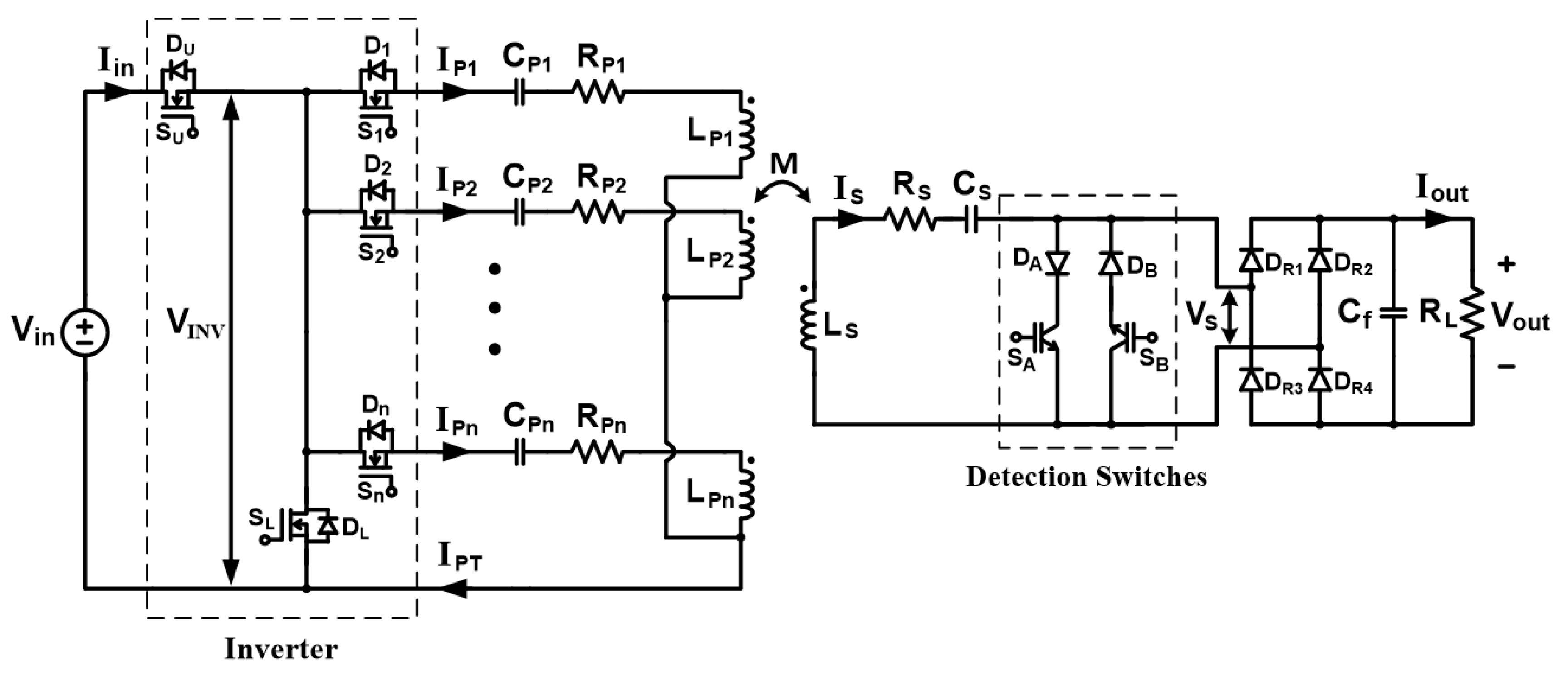
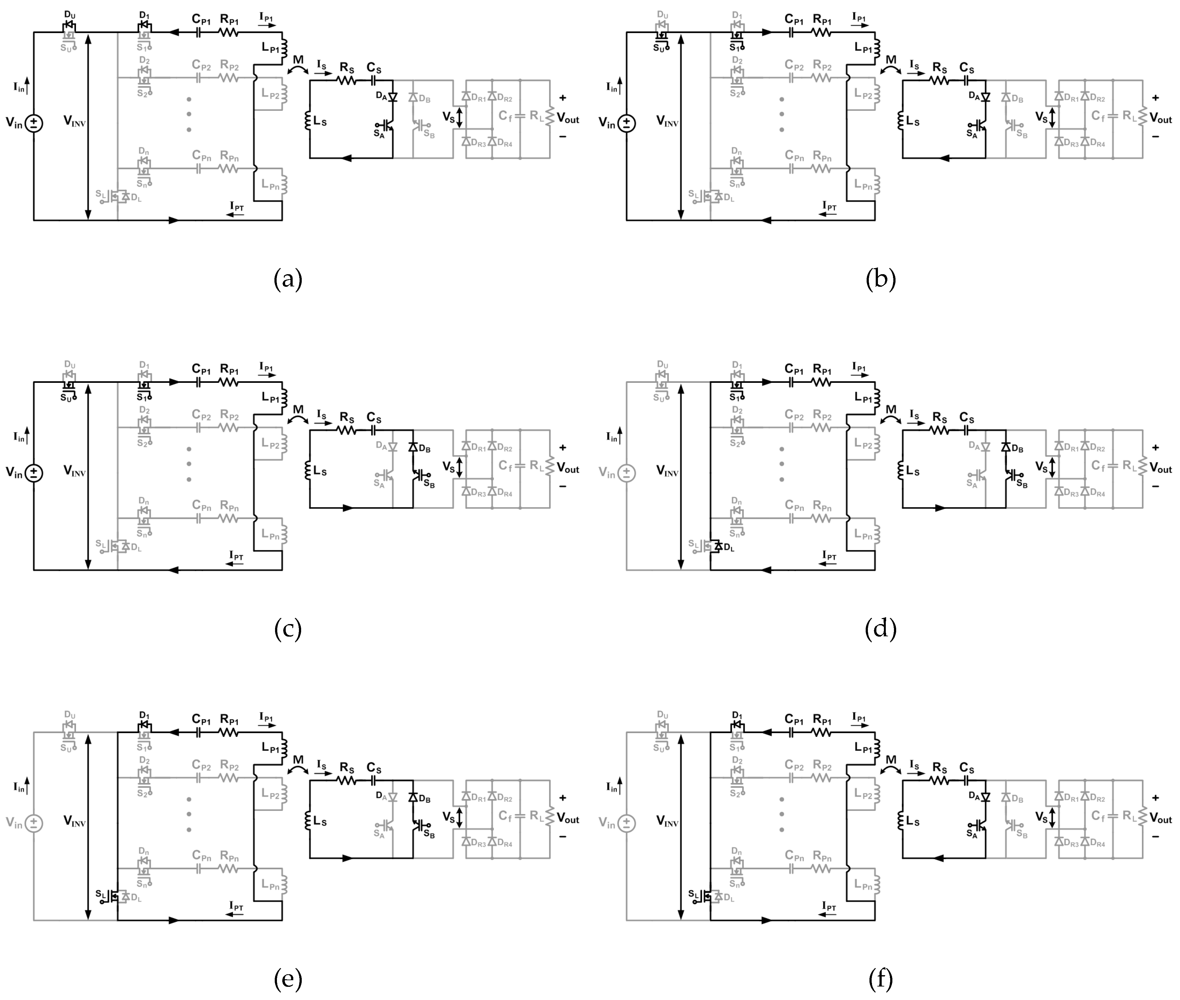
2.1. Circuit Configuration

A block diagram of the proposed system is shown in Figure 1. Multiple transmitter coils are excited by the inverter circuit. Detection switches are placed between the receiver coil and the rectifier circuit. The DC output voltage (Vout) is sensed and transmitted to the primary circuit via wireless communication devices. The primary-side controller is used to select the transmitter coil pattern and regulate the output voltage. The secondary-side controller is used to control the detection switches and send feedback data wirelessly. The circuit configuration of the proposed system is shown in Figure 2. The inverter circuit consists of (n+2) MOSFET switches with antiparallel diodes (DU, DL, D1, D2, …, and Dn), where “n” is the number of transmitter coils. The main upper and lower switches are represented by SU and SL, respectively. The excitation of each transmitter coil is controlled by excitation switches, S1 to Sn. The self-inductance and winding resistance of each transmitter coil are denoted by LP1 to LPn and RP1 to RPn, respectively. Compensation capacitors (CP1 to CPn) are connected in series with each transmitter coil. The mutual inductance between coupled coils is represented by M. LS and RS are the self-inductance and winding resistance of the receiver coil, respectively. CS is the series compensation capacitor. A rectifier circuit with four diodes (DR1 to DR4) and a filter capacitor (Cf) are included on the output. The load is represented by RL. The detection switches are located in front of the rectifier circuit. When they are on, LS and CS form a resonant configuration. With a proper switching frequency on the primary side, the secondary circuit experiences a line commutation. The detection switches are designed to exhibit the bidirectional-carrying and bidirectional-blocking characteristics, which make them similar to an ideal switch.
A combination of two IGBTs (SA and SB) with external diodes (DA and DB) in reverse connection is adopted for the detection switches. The reverse diodes provide reverse-blocking capability to prevent the IGBTs being turned on from negative voltages. The current flowing in each transmitter coil are denoted by IP1 to IPn. The total current in the primary circuit is obtained as:
I P T = I P 1 + I P 2 + + I P n

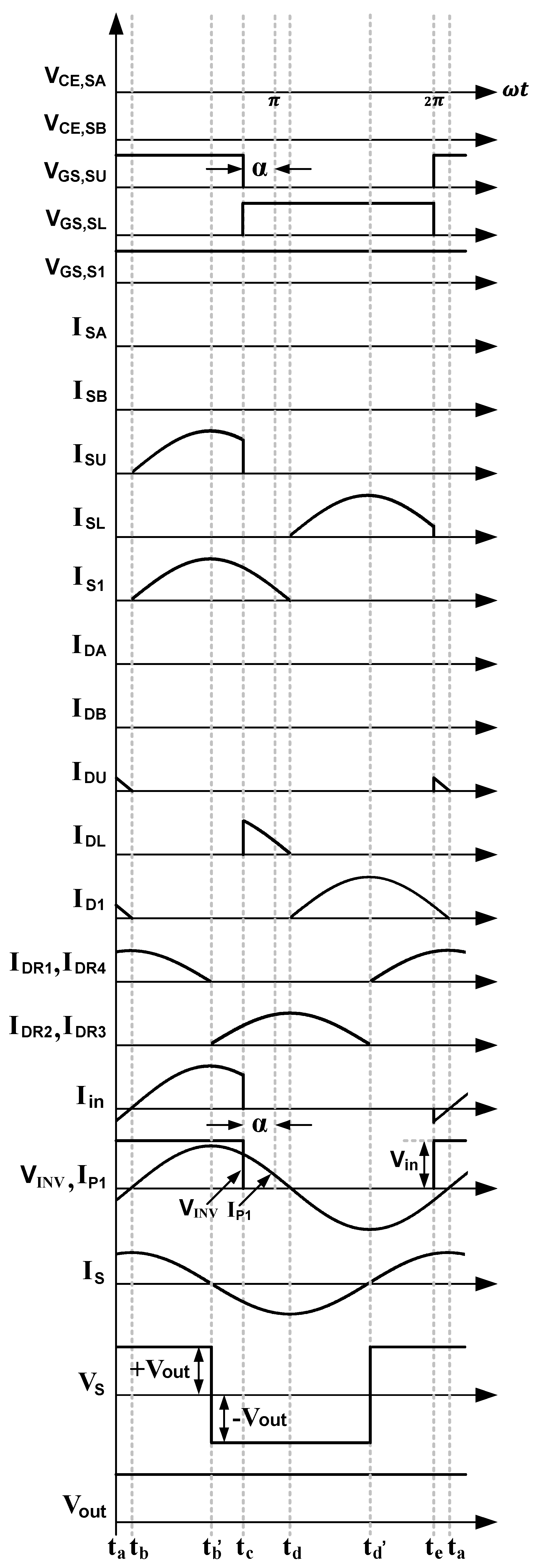
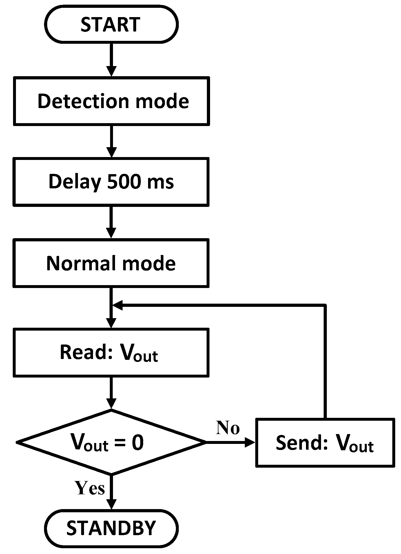
2.2. Mode of Operation

The proposed system is operated in two modes, namely normal mode and detection mode. Both modes are dependent on the operation (on and off) of detection switches. The timing diagram and theoretical waveforms are given to describe the switching operations of both modes. The upper and lower switches (SU and SL) work in the complementary manner. The angle α is defined as the adjusting angle of an inverter voltage, which can be varied from 0 to 180 degrees by adjusting the duty cycle of the upper switch’s gate signal (VGS,SU). For simplicity, all the power switches are assumed to be ideal, and the dead time between switch SU and SL is neglected.

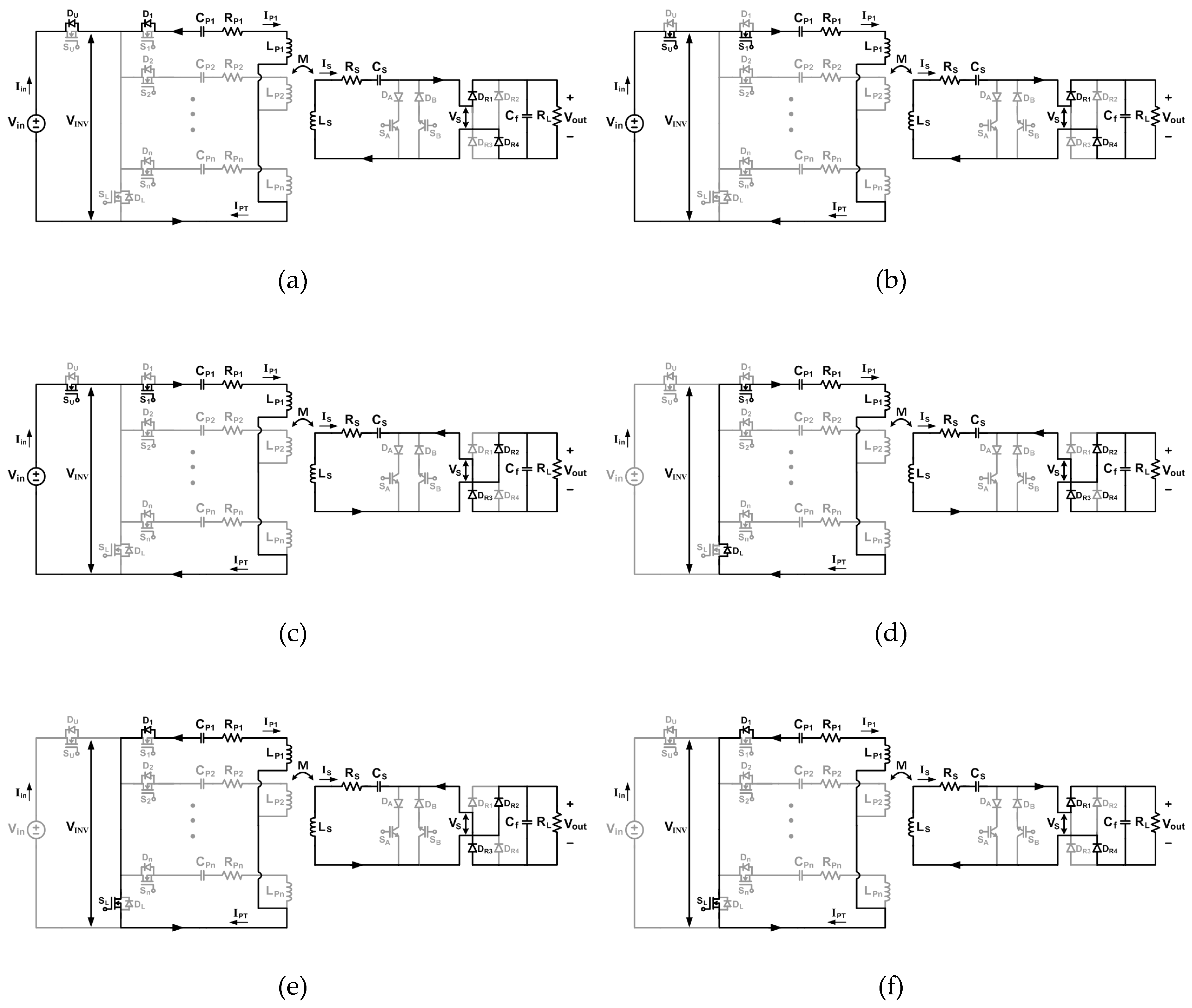
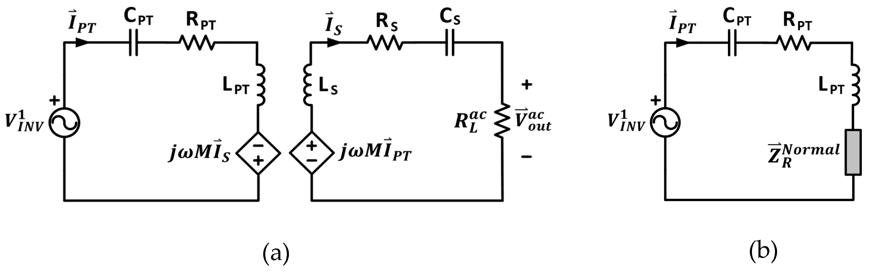
2.2.1. Normal Mode Operation

The normal mode operation is initiated when the detection switches, SA and SB, are turned off. The timing diagram and theoretical waveforms for the case when the excitation switch S1 is turned on are depicted in Figure 3. Only transmitter coil number 1 (LP1) is energized. If two or more coils are energized at the same time, a parallel connection of the energized coils is formed. The resulting circuits of each stage are shown in Figure 4.
Stage 1 [ta–tb] in Figure 3: Both upper and lower switches, SU and SL, are off. The transmitter current IP1 flows in the negative direction through antiparallel diodes D1 and DU. The inverter voltage ( V I N V ) is equal to the DC input voltage ( V i n ). The secondary current (IS) flows in the positive direction, where diodes DR1 and DR4 are turned on. The secondary voltage (VS) is identical to the DC output voltage (Vout).
Stage 2 [tb–tb] in Figure 3: The upper switch SU starts conducting at t = tb, and the current IP1 starts flowing in the positive direction through switches SU and S1. The secondary current, IS, flows in the positive direction and reduces to zero at t = tb.
Stage 3 [tb–tc] in Figure 3: The current IP1 still flows in the positive direction through the switches SU and S1. At t = tb, the secondary current IS starts flowing in the negative direction through diodes DR2 and DR3. The secondary voltage VS becomes negative with opposite polarity to the output voltage (–Vout). The upper switch SU is turned off at t = tc.
Stage 4 [tc–td] in Figure 3: The lower switch SL is still off. The positive current IP1 flows through the switch S1 and the antiparallel diode DL. The inverter voltage V I N V is equal to zero. The secondary current, IS, still flows in the negative direction through diodes DR2 and DR3.
Stage 5 [td–td] in Figure 3: The lower switch SL starts conducting at t = td, and the current IP1 starts flowing in the negative direction through the switch SL and the antiparallel diode D1. The secondary current, IS, still flows in the negative direction.
Stage 6 [td–te] in Figure 3: The current IP1 flows in the negative direction through the switch SL and diode D1. At t = td, the secondary current, IS, starts flowing in the positive direction through DR1 and DR4. The secondary voltage VS is changing from negative to positive value. At t = te, the lower switch SL is turned off. The operation of one switching period is completed. Then, the switching operation is repeated, starting from stage 1.
From fundamental harmonic approximation (FHA), a simplified equivalent circuit of the system under the normal mode of operation is shown in Figure 5. The fundamental component of the inverter voltage ( V I N V ) is denoted by V I N V 1 , and its amplitude can be expressed as:
| V I N V 1 | = V i n 2 + 2 cos ( α ) π
The operating angular frequency is denoted by ω. LPT and RPT represent the equivalent self-inductance and winding resistance of multiple transmitter coils, regardless of the number of coils connected in parallel. The total compensation capacitance in the primary circuit is defined as CPT. The equivalent AC resistance of the load and rectifier circuit [30] is defined as:
R L a c = 8 R L π 2
The reflected impedance, Z R N o r m a l , as shown in Figure 5b, is given as:
Z R N o r m a l = ω 2 M 2 [ R S + R L a c j ( ω L S 1 / ω C S ) ] [ ( R S + R L a c ) 2 + ( ω L S 1 / ω C S ) 2 ]
The total transmitter coil current, I P T , is obtained by:
I P T = V I N V 1 R P T + j ( ω L P T 1 / ω C P T ) + Z R N o r m a l
The magnitude of the equivalent AC output voltage, | V o u t a c | , is expressed as:
| V o u t a c | = ω M R L a c | I P T | | Z S |
where Z S = R S + R L a c + j ( ω L S 1 ω C S ) . The DC output voltage in Figure 2 is obtained as:
V o u t = | V o u t a c | R L 2 R L a c = R L R L a c ω M V i n | Z S | [ 2 + 2 cos ( α ) ] ( 1 / 2 ) 2 π [ δ 2 + λ 2 ] ( 1 / 2 )
where δ = R P T | Z S | 2 + ω 2 M 2 ( R S + R L a c ) and λ = | Z S | 2 ( ω L P T 1 ω C P T ) ω 2 M 2 ( ω L S 1 ω C S ) .
The DC output voltage in Equation (7) can be regulated by adjusting the angle α , which can be realized by controlling the duty cycle of the gate signal of the upper switch, SU.
Note that three out of six switching operations in Figure 4, namely stages 4, 5, and 6, are in the free-wheeling mode. Even though the inverter voltage is equal to zero, the fundamental component of the inverter voltage remains sinusoid. With the resonant compensation arrangement, the system exhibits a high-quality factor (Q) circuit behavior. Only the fundamental component of the inverter voltage in Equation (2) contributes to the current flowing in the circuit. Therefore, the power transfer to the load is provided as:
P o u t = R L a c ω 2 M 2 V i n 2 | Z S | 2 [ 2 + 2 cos ( α ) ] 2 π 2 [ δ 2 + λ 2 ]
The transfer efficiency is slightly decreased when the system is operated in the free-wheeling mode due to the additional turn-off switching loss at t = tc, as shown in Figure 3.

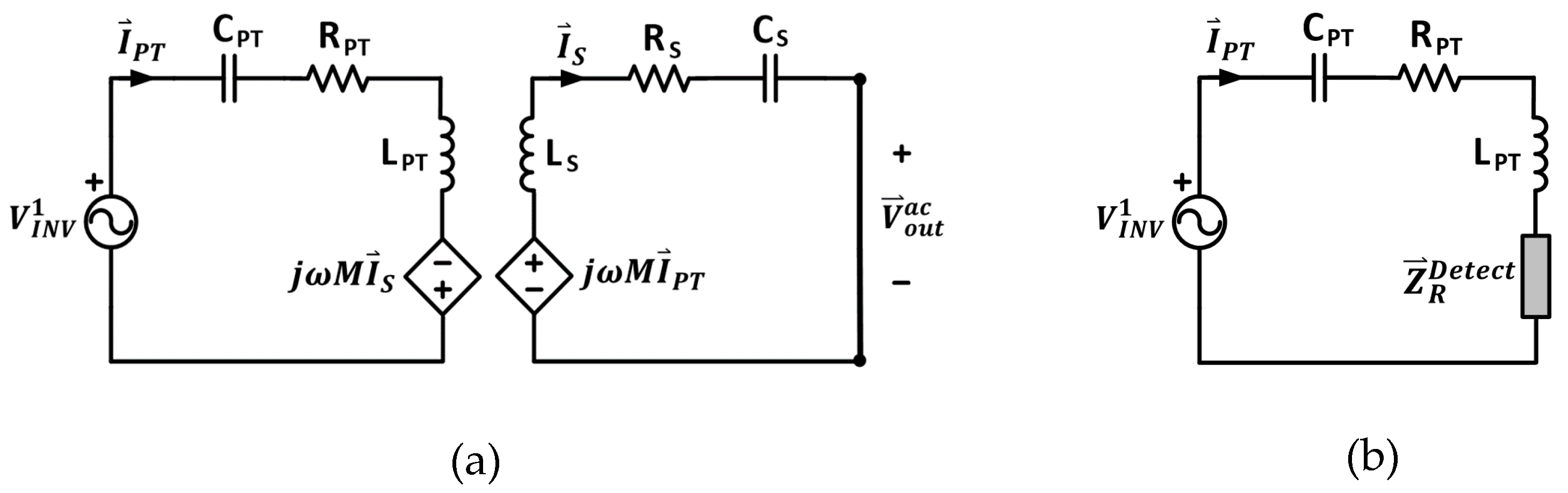
2.2.2. Detection Mode

The detection mode serves as an approach in determining a proper transmitter coil pattern before the charging process. This mode starts with turning switches SA and SB on. The timing diagram and theoretical waveforms of the detection mode are depicted in Figure 6, for the case when the excitation switch S1 is turned on. Only the current IP1 flows through the transmitter coil LP1. Note that the detection operation is performed on each transmitter coil to collect the necessary current information for the determination of a proper coil pattern. Since the detection switches, SA and SB, are turned on throughout the detection process, the secondary voltage VS and output voltage Vout are essentially zero. The switching operation of each stage of the detection mode is shown in Figure 7.
Stage 1 [ta–tb] in Figure 6: Both upper and lower switches, SU and SL, are off. The input current, Iin, is equal to the transmitter current, IP1, and flows in the negative direction through antiparallel diodes D1 and DU. The inverter voltage, V I N V , is equal to the DC input voltage V i n . The secondary current, IS, flows in the positive direction through detection switch SA and diode DA.
Stage 2 [tb–tb] in Figure 6: The upper switch SU starts conducting at t = tb. The current IP1 becomes positive and flows through switches SU and S1. The secondary current, IS, is reduced to zero at t = tb.
Stage 3 [tb–tc] in Figure 6: The switches SU and S1 remain on, and the current IP1 is still positive. The negative current IS flows through the switch SB and diode DB. The switch SU is turned off at t = tc.
Stage 4 [tc–td] in Figure 6: The lower switch SL is still off. The positive current IP1 flows through the switch S1 and the antiparallel diode DL. The secondary current, IS, still flows in the negative direction.
Stage 5 [td–td] in Figure 6: The switch SL has been on. At t = td, the negative current IP1 flows through the switch SL and the antiparallel diode D1. The secondary current, IS, still flows in the negative direction.
Stage 6 [td–te] in Figure 6: The current IP1 flows in the negative direction through the switch SL and diode D1. At t = td, the switch SA and diode DA conduct positive current IS. The lower switch SL is then turned off at t = te. The operation of one switching period is completed. The next switching cycle is repeated starting from stage 1.
A simplified equivalent circuit for detection mode operation is shown in Figure 8. Clearly, the equivalent AC output voltage, V o u t a c , is equal to zero. The reflected impedance, Z R D e t e c t , as shown in Figure 8b, is given as:
Z R D e t e c t = ω 2 M 2 [ R S j ( ω L S 1 / ω C S ) ] [ R S 2 + ( ω L S 1 / ω C S ) 2 ]
Due to the absence of the equivalent AC resistance ( R L a c ), the reflected impedance Z R D e t e c t is significantly larger than the reflected impedance under normal operation in Equation (4). This means that the primary current ( I P T ) is considerably lower. With the knowledge of the current in each transmitter coil, the position of the receiver coil can be estimated, and a proper transmitter coil pattern is obtained.

3. Transmitter Coil Excitation

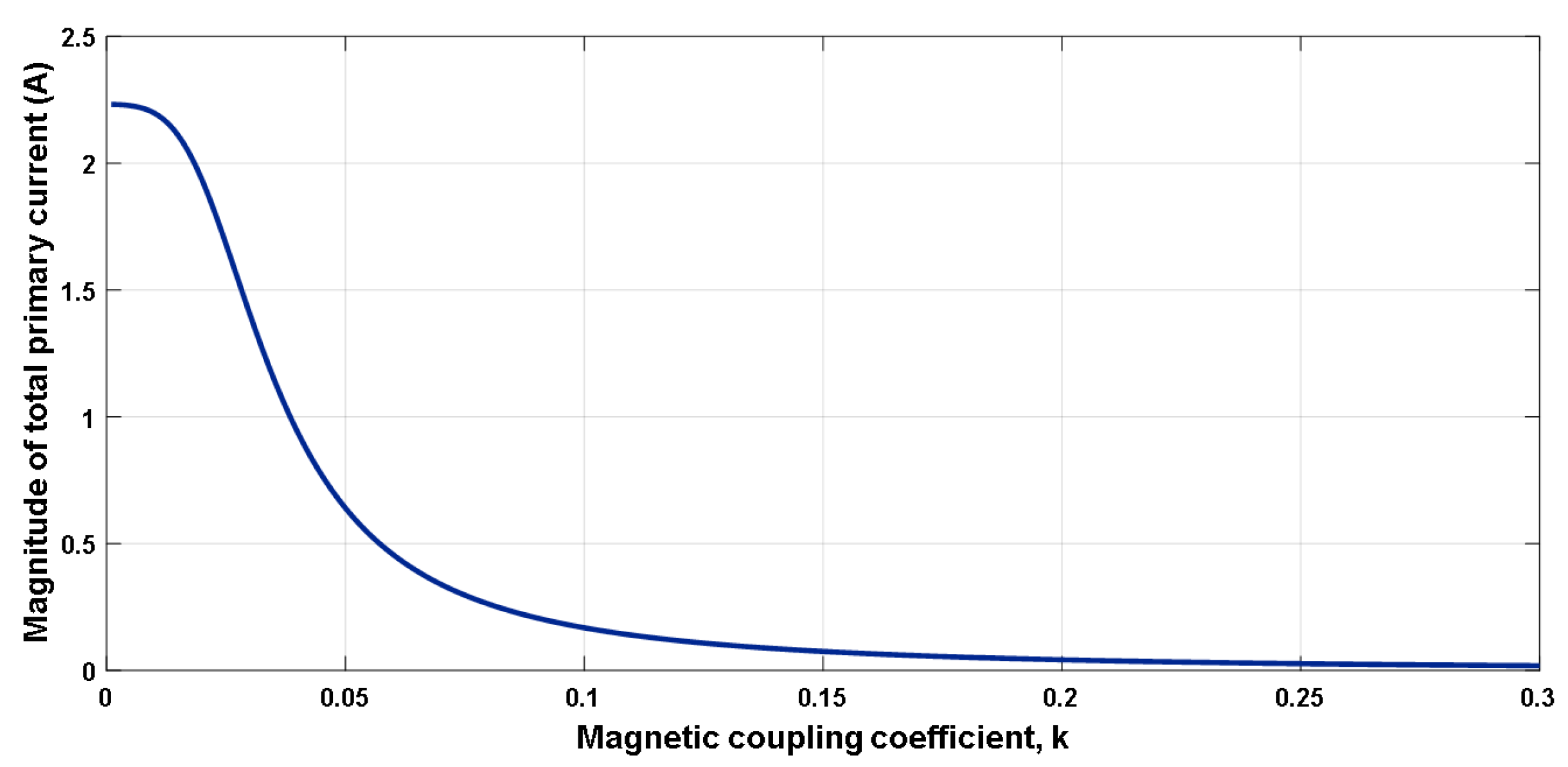
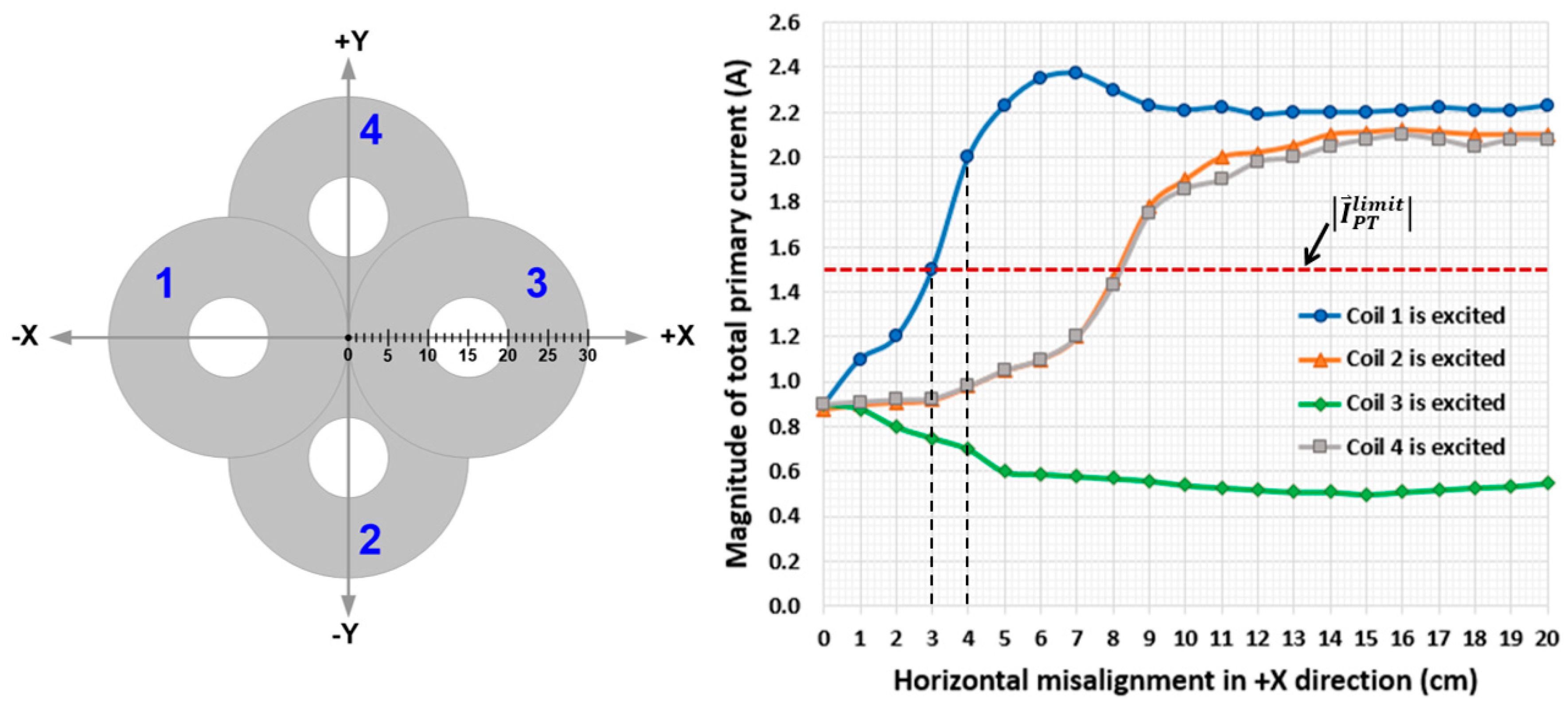
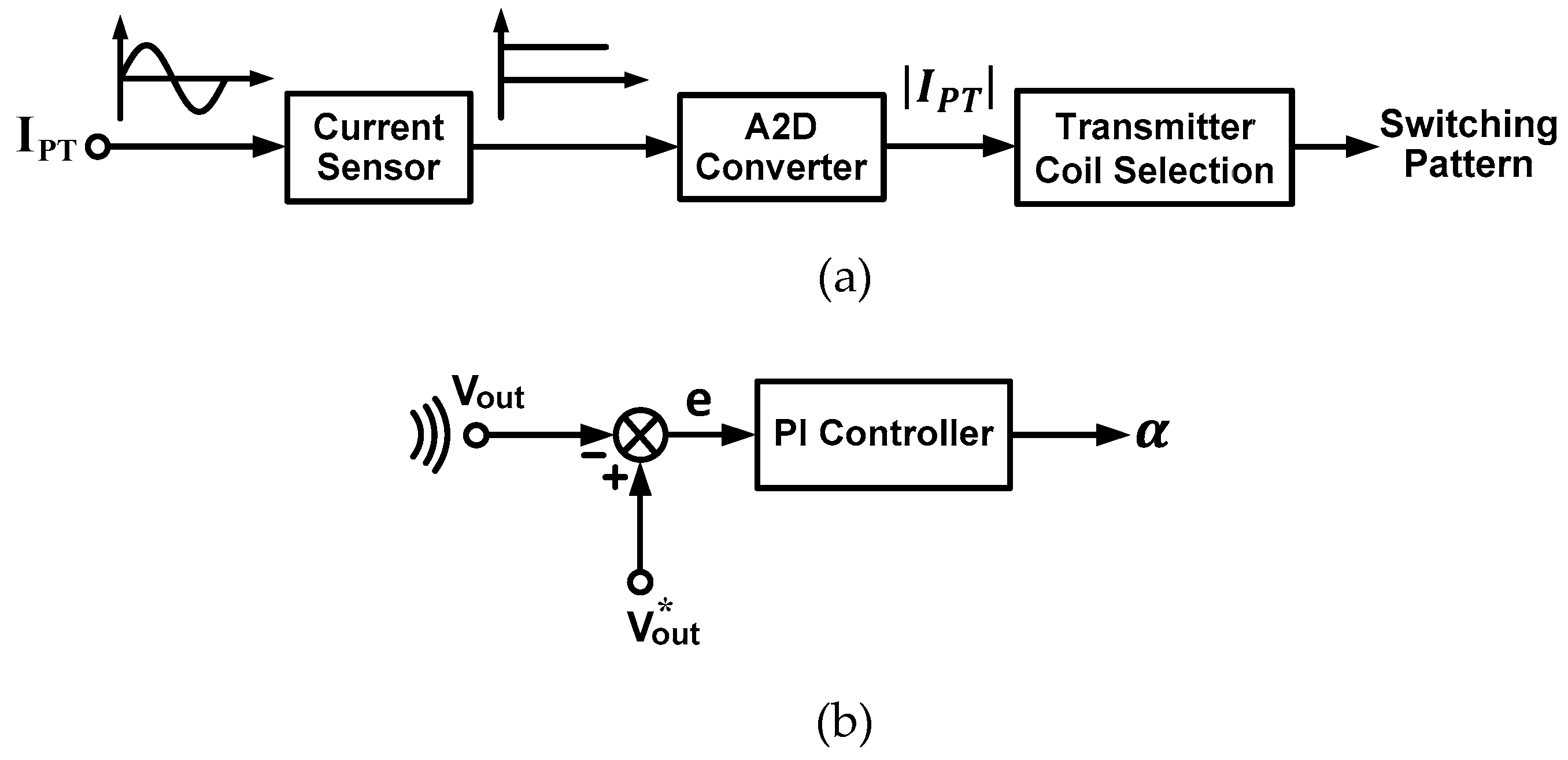
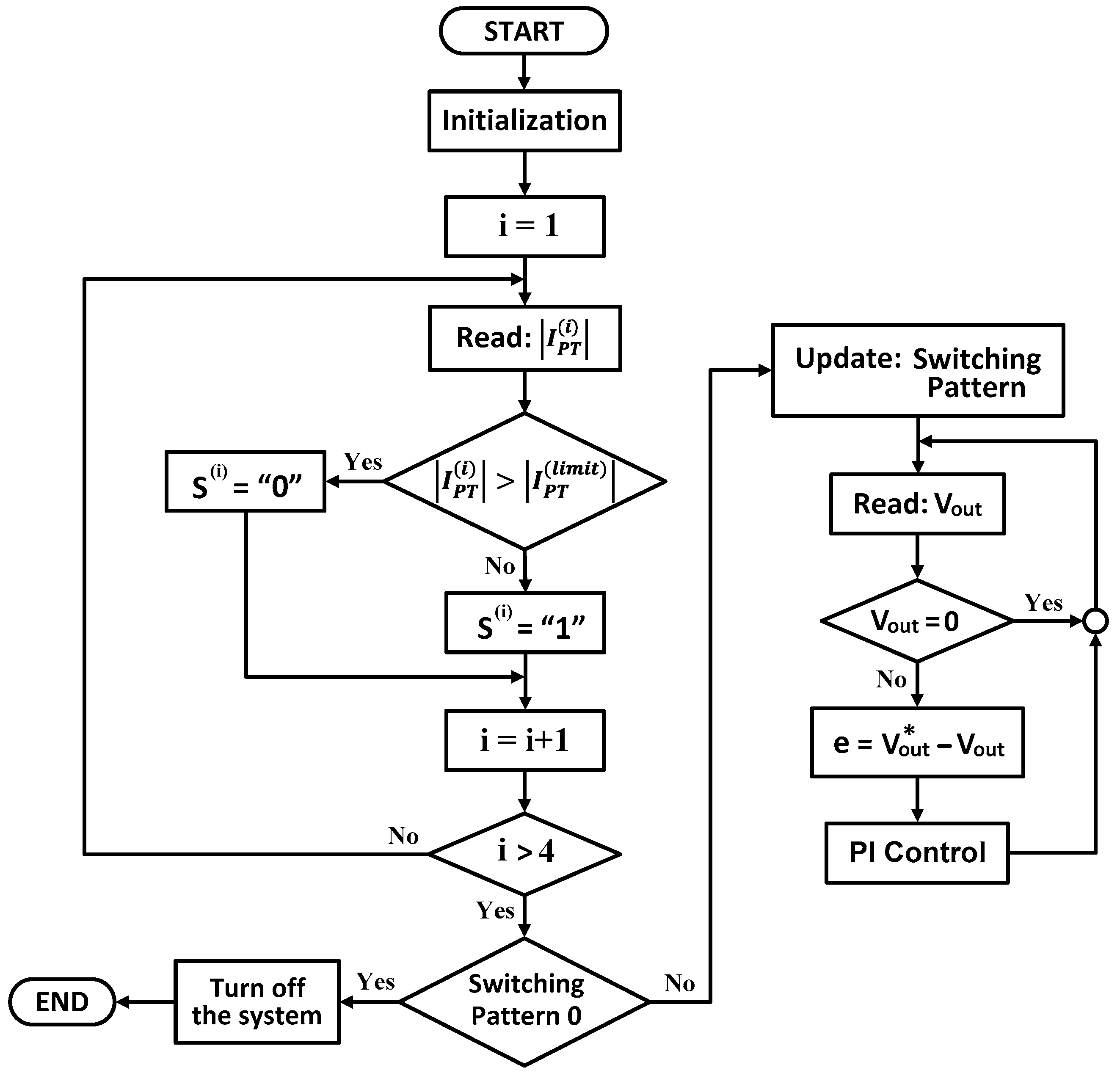
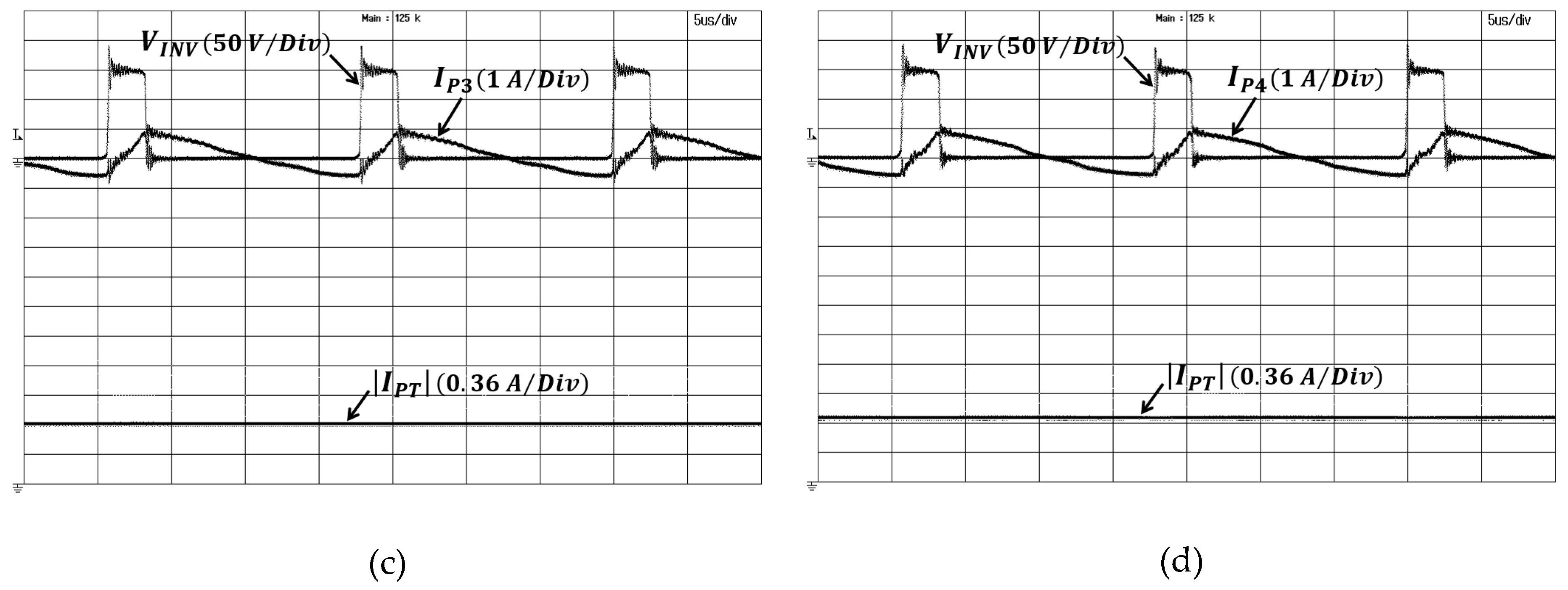
3.1. Detection of Receiver Coil Position

An important benefit of a WPT multi-coil system is the free-positioning feature, where the receiver coil can be placed freely in a designated area and may be coupled with one or more transmitter coils at a time. The coupled coil used in the proposed WPT multi-coil system is shown in Figure 9. In this work, four identical coils are adopted as multiple transmitter coils (n = 4) with a single receiver coil. The transmitter coils are arranged based on the comparative study reported in [31], where high misalignment tolerance is obtained. The mutual inductance (M) and magnetic coupling coefficient (k) between the transmitter and receiver coils are dependent on the position of the receiver coil. Theoretically, only the directly coupled transmitter coil or set of transmitter coils should be excited. For the same air gap or vertical distance between coupled coils, the magnetic coupling is maximized at the aligned position, where both coils share the same center. The coefficient k is decreased as the horizontal distance between both coils is increased. In the detection mode, the magnitude of the total primary current ( | I P T | ) depends on the coupling coefficient as:
| I P T | = | V I N V 1 | [ ( R P T + ω 2 k 2 L P T L S R S [ R S 2 + ( ω L S 1 / ω C S ) 2 ] ) 2 + ( ω L P T 1 ω C P T ω 2 k 2 L P T L S ( ω L S 1 / ω C S ) [ R S 2 + ( ω L S 1 / ω C S ) 2 ] ) 2 ] ( 1 / 2 )
Then, the receiver coil position can be calculated through the total primary current obtained during the detection mode operation, as discussed in Section 2.2.2. The relationship between the total primary current and the coupling coefficient in Equation (10) is illustrated in Figure 10, using the following parameters: LPT = 280 µH, LS = 1.37 mH, RPT = 0.33 Ω, RS = 2.03 Ω, CPT = 32.57 nF, CS = 5.4 nF, f = 58.51 kHz, Vin = 150 V, and α = 126 ° . Clearly, | I P T | is decreasing as the magnetic coupling k is increased. A comparison of the transmitting current in each coil yields an approximated position of the receiver coil. For example, if the | I P T | value of transmitter coil 3 is significantly lower than the currents obtained from transmitter coils 1, 2, and 4, the receiver coil is located close to the center of transmitter coil 3, as shown in Figure 11a. If the receiver coil is placed between coil number 3 and 4, as shown in Figure 11b, the | I P T | values of both coils are almost identical, but substantially lower than the | I P T | value obtained from coil numbers 1 and 2 from the other end.

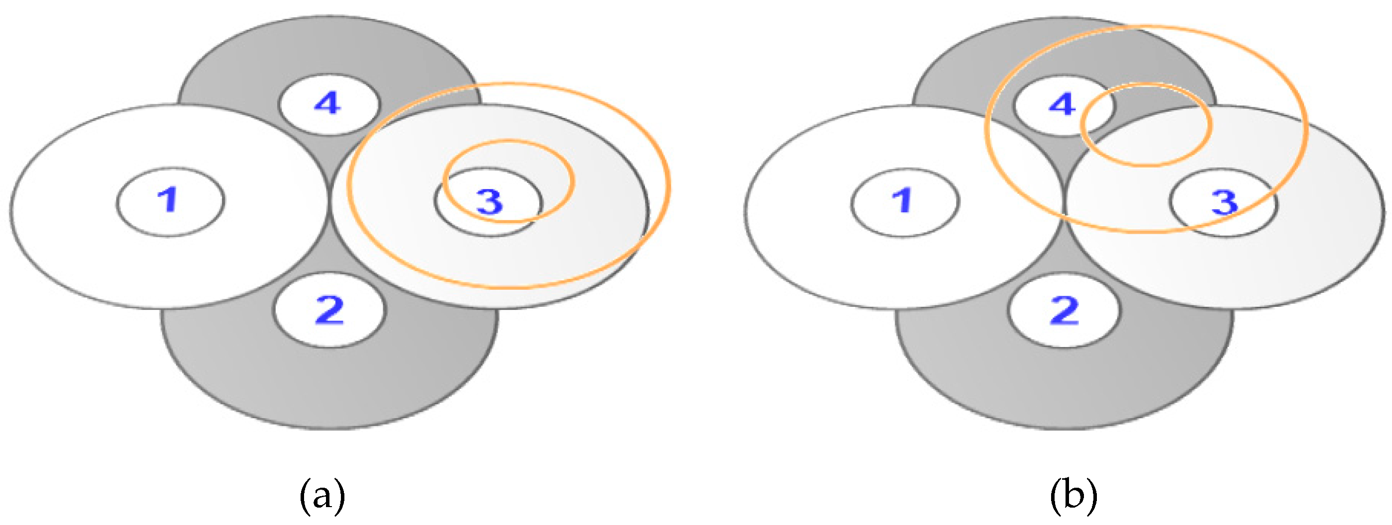
3.2. Transmitter Coil Pattern Selection

Each transmitter coil in the proposed system can be excited separately or simultaneously, depending on the switching pattern of the excitation switches (S1–S4) of the proposed inverter circuit, as listed in Table 1. The values of the switching function, “1” and “0”, indicate that the excitation switches are turned on and off, respectively. This results in 16 transmitter coil patterns, corresponding with the activated coil. For efficient power transfer, transmitter coils pattern with weakly coupling coefficients should not be energized. Only the tightly coupled transmitter coil pattern, which is defined as the proper transmitter coil pattern, is excited. The proper coil pattern generally gives the highest magnetic coupling available, which maximizes the transfer efficiency of the WPT system. The proposed selection of the transmitter coil pattern is based on the obtained current | I P T | from the detection operation. Initially, the current | I P T | is measured as the receiver coil is laterally moved along the +X direction, as shown in Figure 12. When the receiver coil position is changed from 3 to 4 cm, the | I P T | value obtained from transmitter coil 1 is increased from 1.5 to 2 A, which is the highest rate of change of | I P T | . This means that the magnetic coupling between transmitter coil 1 and the receiver coil is greatly reduced at this point. The current of 1.5 A is empirically imposed as the current limit value, | I P T l i m i t | , for the excitation decision of each of the transmitter coils. The proposed coil selection procedure is outlined as follows. First, each transmitter coil is excited at a time. The magnitude of the transmitter current in each coil is identical to | I P T | in this case. Then, each measured transmitter current is compared with | I P T l i m i t | . If | I P T | > | I P T l i m i t | , the excitation switch to the activated transmitter coil is set to “0” or turned off, because the magnetic coupling is rather weak, indicating that the receiver coil is located away from the activated transmitter coil. If | I P T | | I P T l i m i t | , the receiver coil is relatively close to the excited coil, and the corresponding excitation switch will be set to “1” or turned on. After the comparison process, the switching pattern for a proper transmitter coil pattern is obtained.

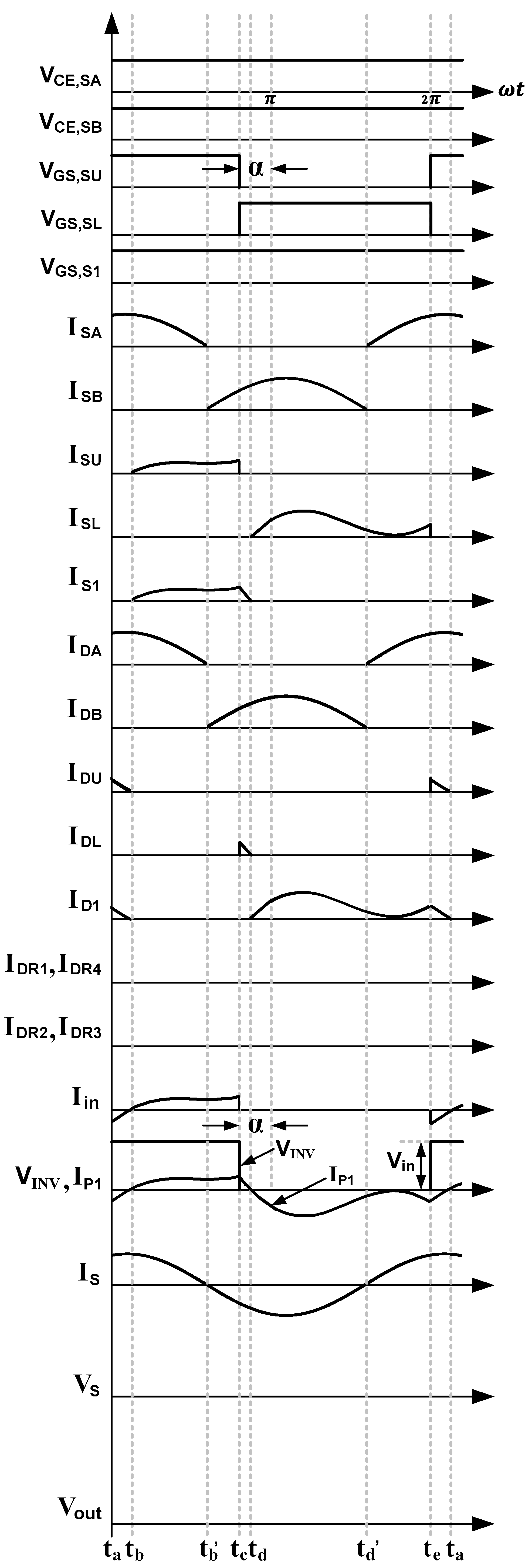
4. Proposed Controller

The control is implemented on both the primary side and the secondary side, as shown in Figure 1. The primary-side controller is adopted to find the proper transmitter coil pattern and regulate the output voltage. The secondary-side controller serves the detection operation and wireless data collection of the output voltage ( V o u t ) to the primary side.

4.1. Secondary-Side Controller

The proposed system is designed for the static WPT applications. In this work, it is assumed that there is no movement of the receiver coil during the charging process. A flowchart diagram of the secondary-side controller is shown in Figure 13. After the receiver coil is placed in a designated area, the controller wakes up from the standby mode. Then, the detection operation is initiated by turning the detection switches on for 500 ms to allow completion of the detection process. Next, the detection switches are turned off for normal mode operation. The output voltage, V o u t , is measured and read. If V o u t = 0 , it means that the receiver coil is absent or the inverter circuit on the primary side is inoperative, and the controller is put into standby mode. The V o u t data will be sent to the primary side if V o u t differs from zero.

4.2. Primary-Side Controller

The proposed control block diagram of the primary-side controller is shown in Figure 14. First, the controller operates in the transmitter coil selection mode, as shown in Figure 14a. Each transmitter coil is energized, one at a time. The current in each transmitter coil is obtained through the measured total primary current, I P T , and sent to the current sensor. A signal conditioner consisting of a rectifier and low-pass filter circuit is included in the current sensor module. The DC signal representing the magnitude of the total primary current, | I P T | , is obtained. The MCU reads the | I P T | signal through the analog to digital (A2D) converter function. Then, the controller starts the coil selection process. All the | I P T | signals collected from each transmitter coil are compared with | I P T l i m i t | , as described in Section 3.2. Then, the switching pattern of the inverter circuit is obtained for a proper transmitter coil pattern corresponding to the receiver coil position. After the selected coil pattern is energized, the controller operates in the output voltage regulation mode, as shown in Figure 14b.
This mode is based on the relationship between the output voltage and angle α of the inverter voltage in Equation (7). The output voltage signal, V o u t , is wirelessly fed back from the secondary side, and compared with the reference value ( V o u t ). The resulting error (e) is sent to the PI controller, and the adjusting angle α is obtained.
The program flowchart of the primary-side controller is shown in Figure 15. At the beginning, the controller operates in the transmitter coil selection process. To prevent excessive current in each transmitter coil, the angle α of 126 degrees is assigned to the upper switch SU. The current limit, | I P T l i m i t | , is set to 1.5 A. Initially, the transmitter coil number 1 (i = 1) is energized by turning the switch S1 on. Then, the current signal | I P T ( 1 ) | is read. If | I P T ( 1 ) | > | I P T l i m i t | , the switching function of the excitation switch ( S ( 1 ) ) is set to “0”; otherwise, it is set to “1”. As the value of “i” is increasing, transmitter coils 2, 3, and 4 take turns energizing. The signals | I P T ( 2 ) | , | I P T ( 3 ) | , and | I P T ( 4 ) | are read and compared with the | I P T l i m i t | . The switching pattern of the inverter circuit is obtained. The pattern 0 is obtained when the receiver coil is placed outside the designated area. That is, the magnetic coupling is too weak, and the system will be turned off. The proper transmitter coil pattern is formed if the switching pattern 1 to 15 is presented. Next, the controller operates in the output voltage regulation process. The output voltage data V o u t is read. If V o u t = 0 , the detection switches are still on, and the system is in the detection mode. The controller will wait until the system is in normal operation mode, where V o u t is not equal to zero. Then, the feedback signal V o u t is compared with the reference signal, V o u t . With the PI controller, the angle α of an inverter voltage is adjusted. The actual output voltage follows the reference value.

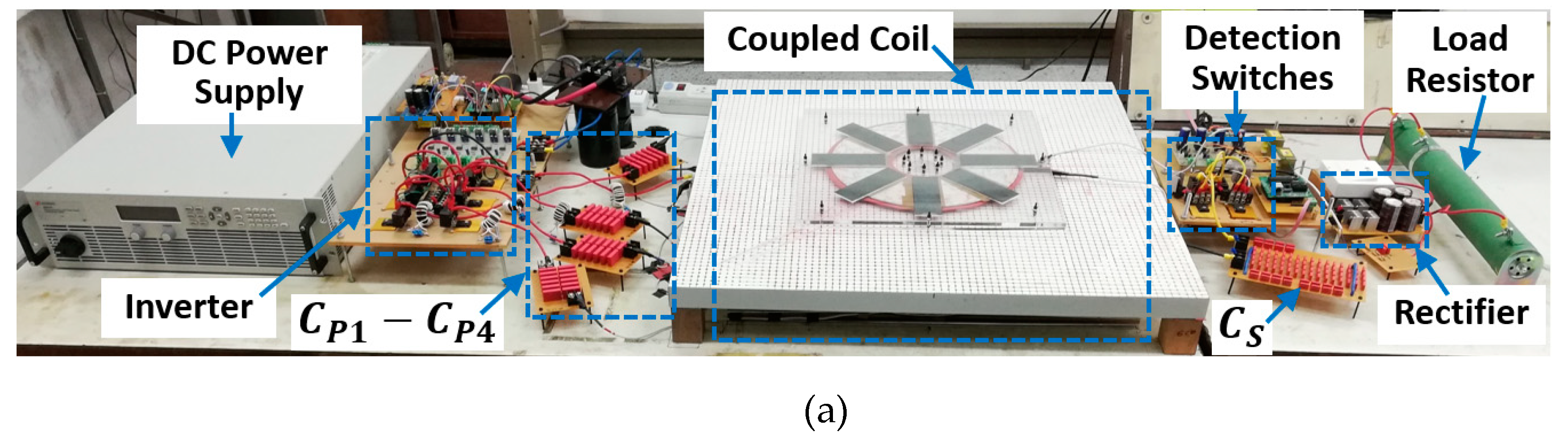
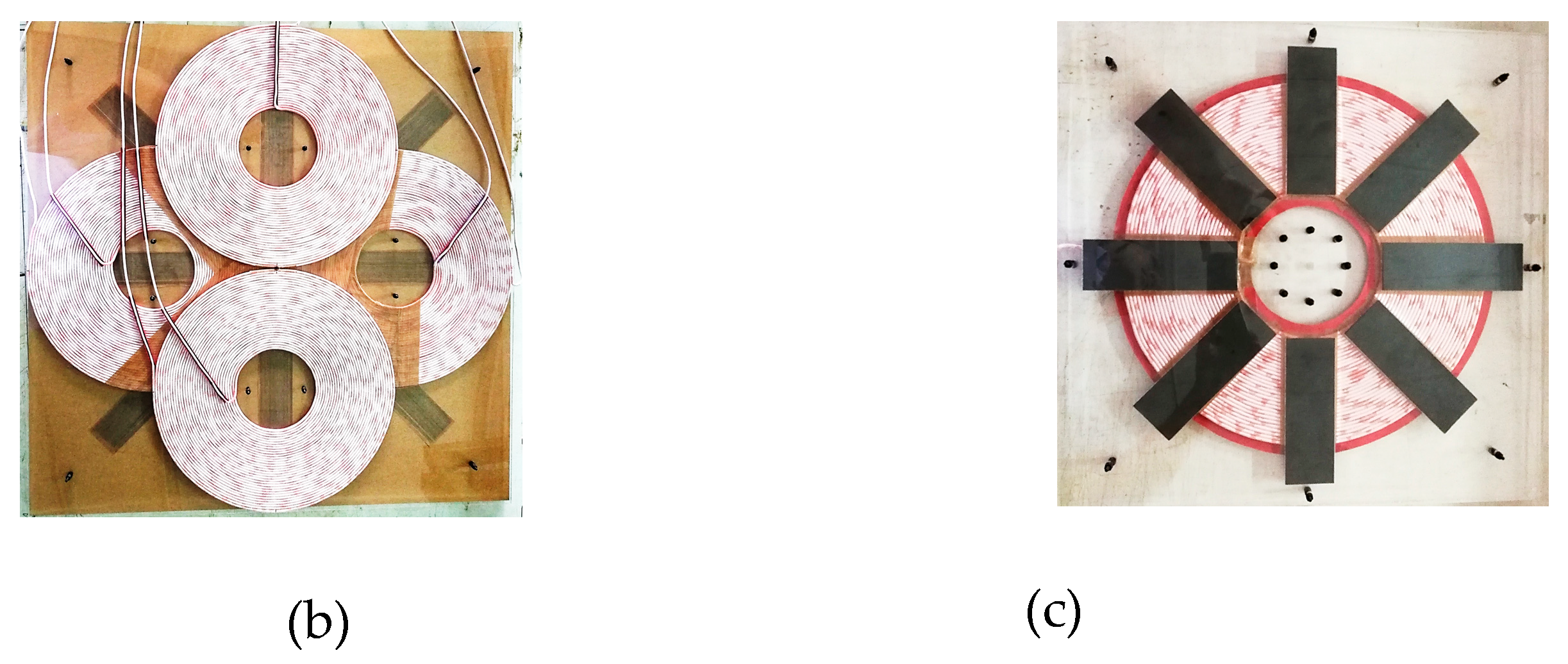
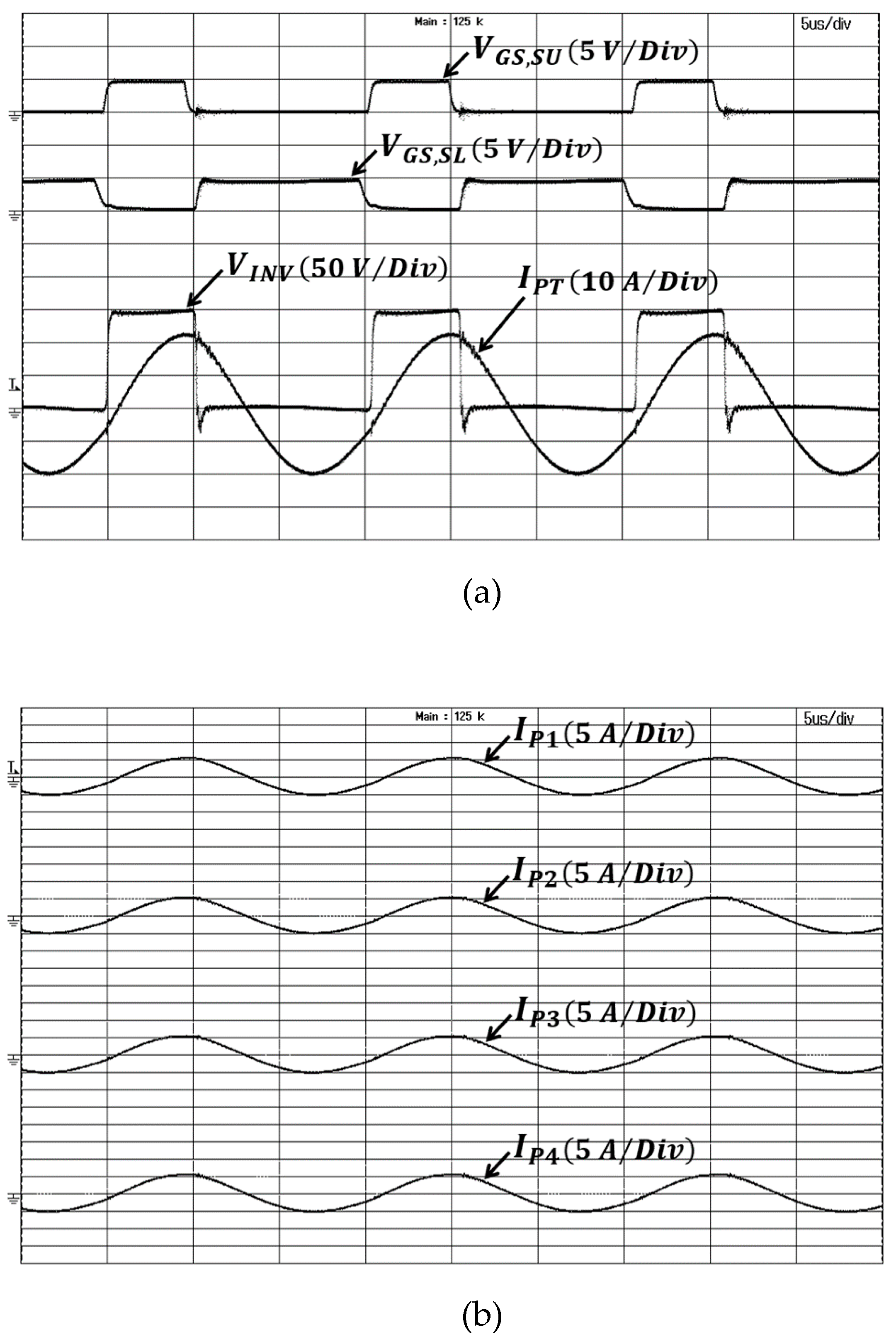
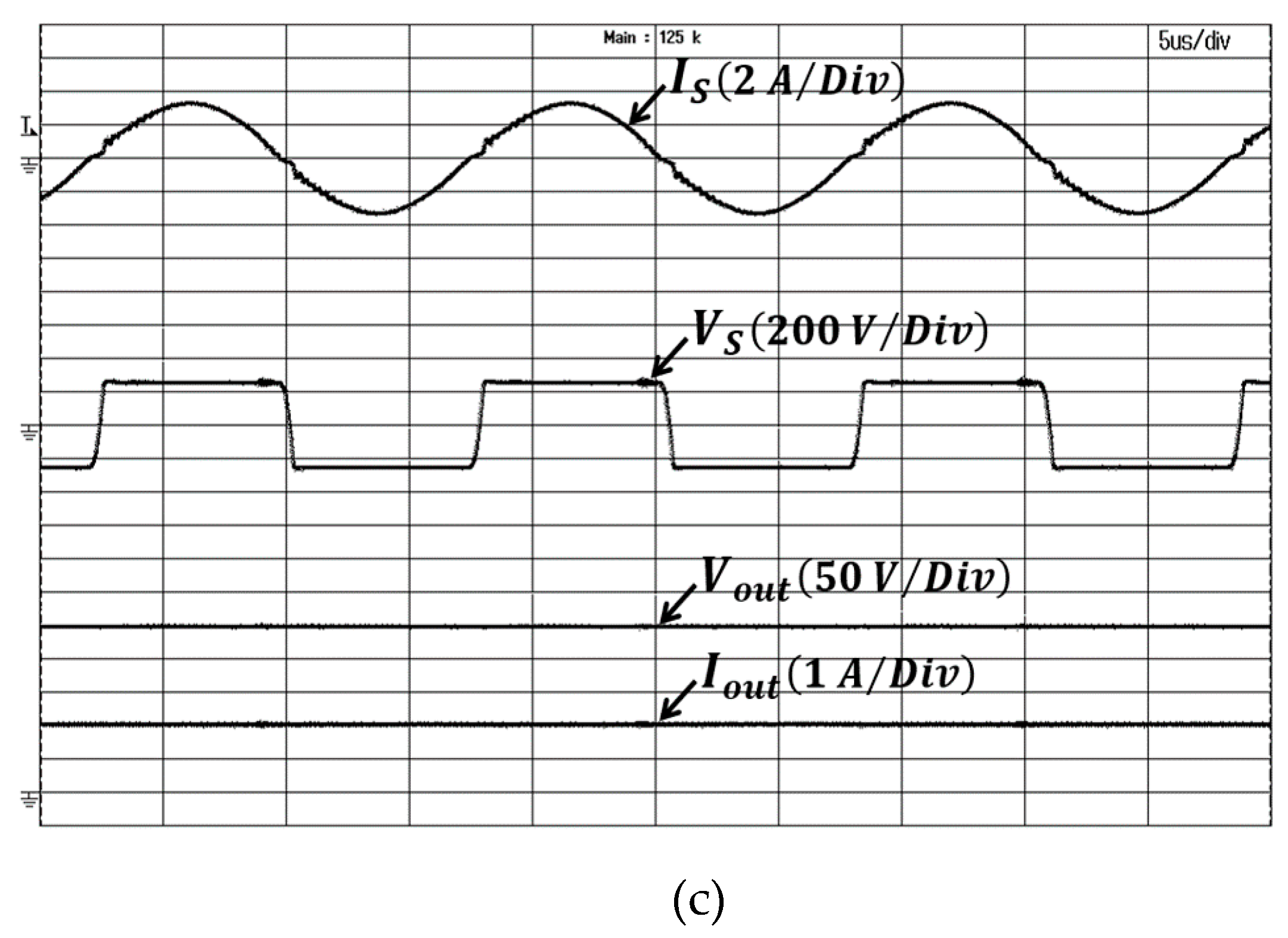
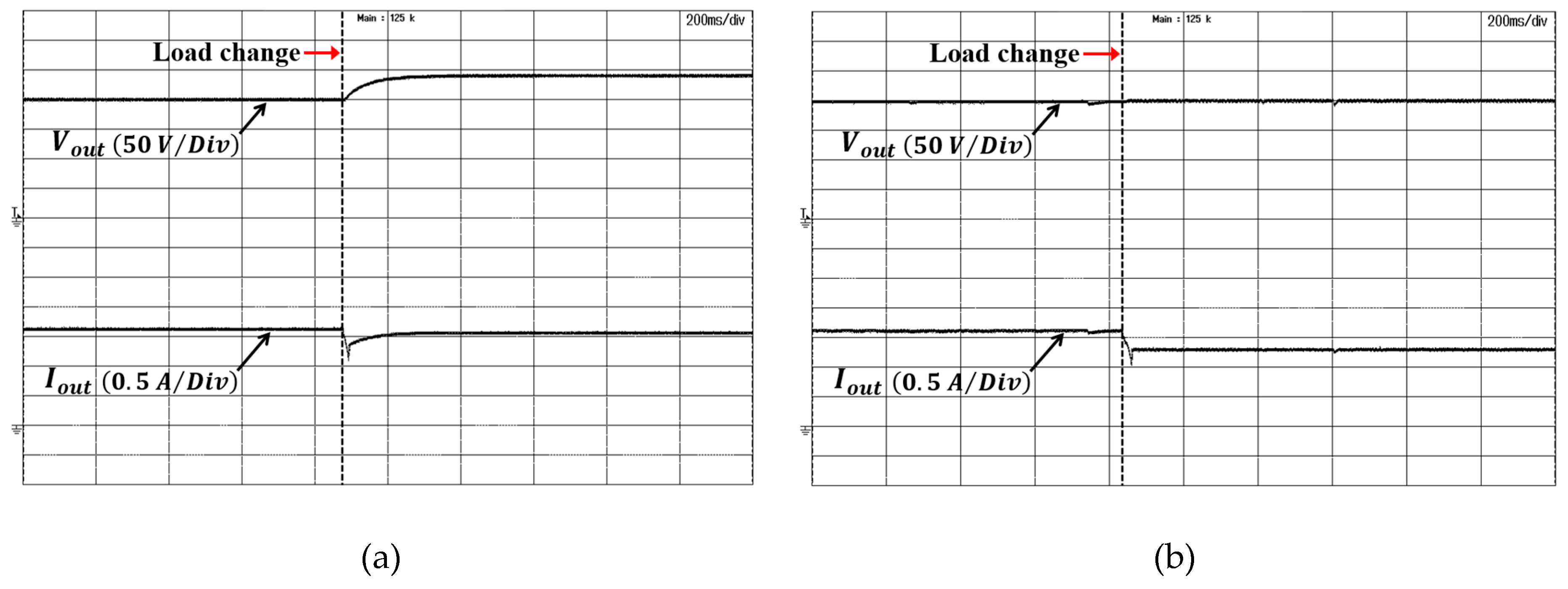
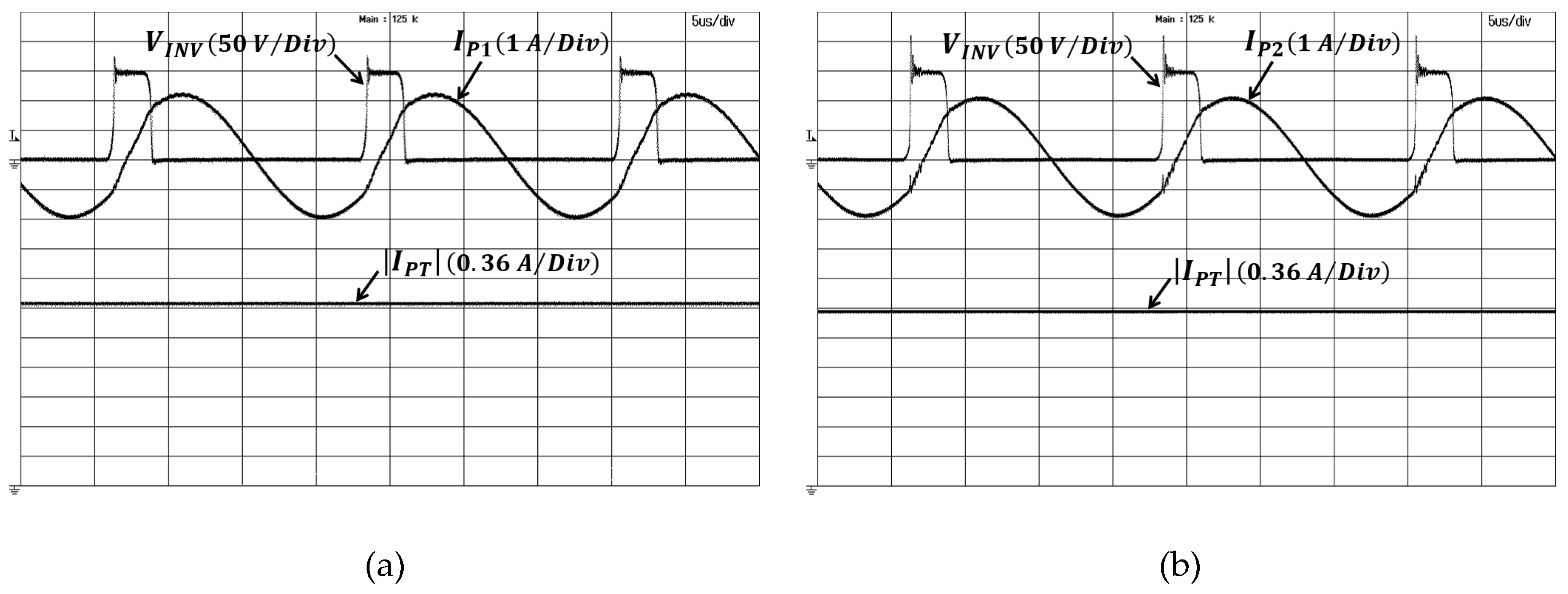
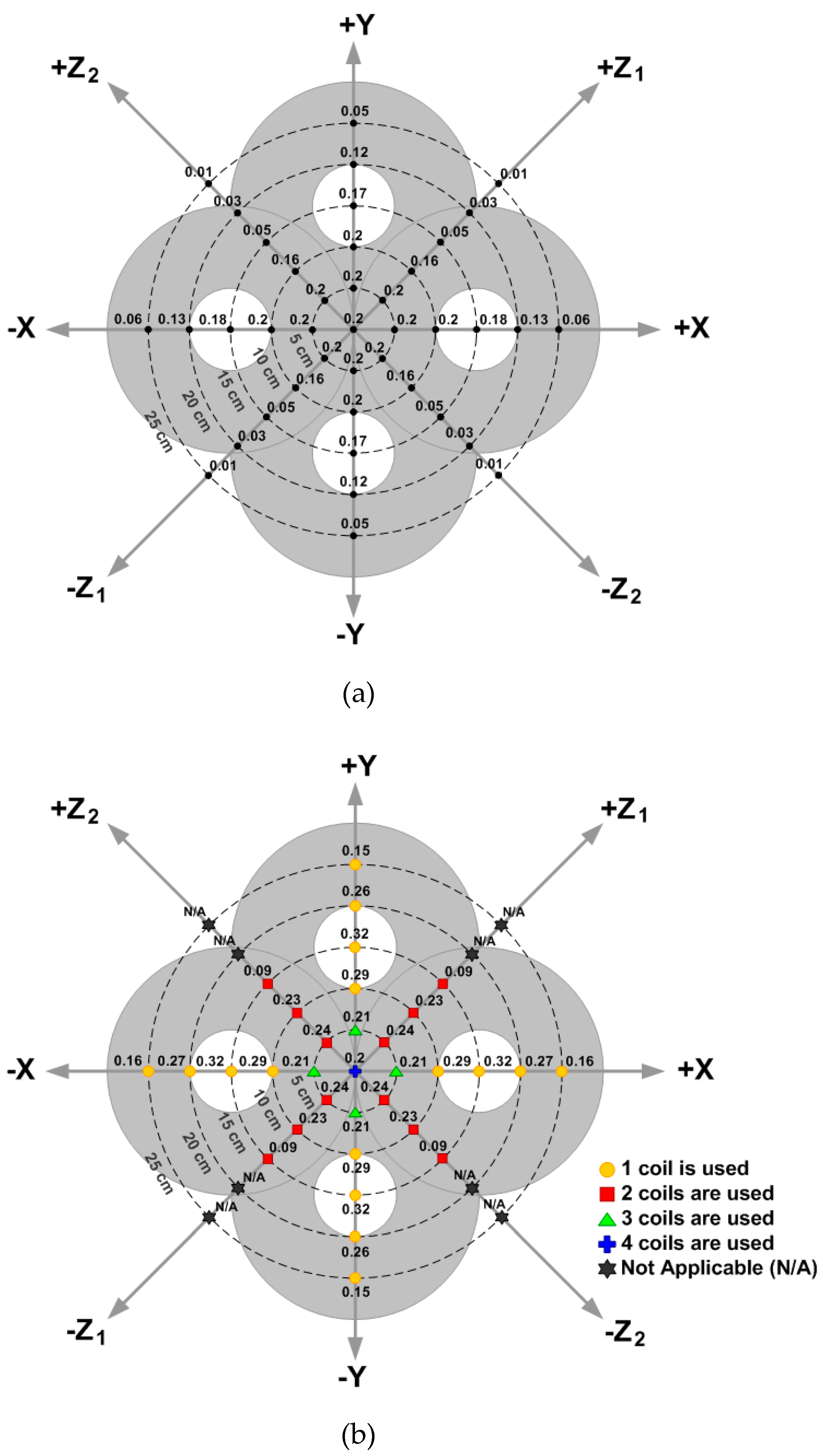
5. Experimental Results

To validate the proposed system, an experimental setup of the WPT multi-coil system is created, as shown in Figure 16. Four identical coils are used as multiple transmitter coils. Each coil is made of 32 turns of litz wire. The inner and outer diameters are 10 cm and 30 cm, respectively. The receiver coil is a two-layer spiral coil with 30 turns of litz-wire for each layer. The inner and outer diameters are 12 cm and 30 cm, respectively. The air gap between the coupled coils is maintained at 10 cm. The transmitter coil is placed in a fixed position, whereas the receiver coil can be laterally moved in a designated area. This results in the horizontal misalignment. The measured circuit parameters are listed in Table 2. The input DC voltage is set to 150 V. The switching frequency is fixed at 58.51 kHz.
Experimental waveforms under normal mode operation are shown in Figure 17. The receiver coil is placed at the center or zero horizontal misalignment. Switching pattern 15 is applied, where all the transmitter coils are energized. The angle α is at 58 degrees. As seen in Figure 17b, the transmitter current in each coil is almost identical in both magnitude and phase.
The summation of all the transmitter coil currents are equal to the total primary current, I P T . From the output voltage V o u t and current I o u t shown in Figure 17c, the output power is obtained as 500 watts.
The results of the output voltage regulation when the load resistance is abruptly changed from 123.2 to 151.2 Ω is shown in Figure 18. The desired output voltage, V o u t , is 200 V. Without the output voltage regulation, the output voltage is rising to 240 V as the load resistance is instantaneously increased, as seen in Figure 18a. With the proposed controller, the output voltage change is negligible and regulated at the desired value, as shown in Figure 18b.
Experimental waveforms under detection mode operation are shown in Figure 19. The receiver coil is moved 10 cm from the center and placed between transmitter coils 3 and 4. Each transmitter coil is energized at a time. The angle α is set to 126 degrees. The output signal from the current sensor, | I P T | , is illustrated. In Figure 19a,b, the | I P T | values of transmitter coils 1 and 2 are 2.2 A and 2.1 A, respectively. These values are greater than the imposed limit | I P T l i m i t | at 1.5 A. This is an indication that the receiver coil is placed far away from both transmitter coils, where the magnetic coupling is weak. Thus, the excitation switches S1 and S2 are off for efficient power transfer. On the other hand, the | I P T | values of transmitter coils 3 and 4 in Figure 19c,d, are 0.72 A and 0.76 A, respectively. This is an indication that the receiver coil is close to both transmitter coils. Therefore, both switches S3 and S4 are turned on. From Table 1, switching pattern 3 is formed as the selected transmitter coil pattern.
The measurement results of magnetic coupling coefficient, k, when the receiver coil was laterally moved along the X, Y, Z1, and Z2 directions, are shown in Figure 20. To illustrate the advantage of the proposed transmitter coil pattern selection, all the transmitter coils were first excited throughout the operation. This is switching pattern 15, and the magnetic coupling k obtained in this case is shown in Figure 20a. The coupling k is at the maximum value of 0.2, as the receiver coil is within a 5-cm radius. If the receiver coil is moved further, the coupling k is reduced to 0.01 at 25 cm on the Z1 and Z2 directions. With the proposed transmitter coil pattern selection, the resulted magnetic coupling is shown in Figure 20b. For the case of one-coil excitation, at 15-cm misalignment along the X and Y directions, the coupling coefficient increased from 0.18 to 0.32, which is a 77.78% improvement compared with results in Figure 20a. For the case of two-coil excitation, the coupling coefficient k increased from 0.16 to 0.23, which was a 43.75% improvement at 10-cm misalignment along the Z direction. Note that “not applicable (N/A)” is the case of switching pattern 0, in which all the transmitter coils were not activated.
System efficiency measurements when the receiver coil is laterally moved along the +X and +Z1 directions are shown in Figure 21a,b, respectively. The load resistance is fixed at 123.2 Ω. The output voltage is regulated at 200 V throughout the operation. The proposed multi-coil system with and without transmitter coil pattern selection is compared. At the center (zero horizontal misalignment), the measured efficiencies for both cases are at 83.63%, since the activated coil patterns are identical. When the misalignment in the +X direction is increased, the efficiency of the system with proposed coil selection is increased to its maximum at 90.1% before decreasing to 74.3% at 25 cm. On the other hand, the efficiency of the system without transmitter coil selection is gradually reduced to 38.21% at 25 cm. Similarly, for the +Z1 misalignment direction, the proposed coil selection yields improved efficiencies of 18.9% and 54.5% at 10 cm and 15 cm, respectively. The efficiency of a single-coil system (single transmitter coil and single receiver coil) is also illustrated. At the aligned position, the efficiency of the single-coil system is at 89.8%. That is 6.87% higher than the multi-coil system due to its higher coupling coefficient. As the horizontal misalignment is introduced, the single-coil system efficiency drastically decreases. At 15-cm misalignment, the efficiency is reduced to 44.1%, no matter the direction of the misalignment. With the proposed multi-coil system, the efficiency is increased to 90.1% (in the +X direction). For the +Z1 misalignment direction, the proposed multi-coil system yields an efficiency improvement of 19.6% and 22.6% at 10-cm and 15-cm misalignments, respectively.

6. Conclusions

The topology of an inverter circuit for driving multiple transmitter coils of a WPT system is presented in this paper, which reduces the component counts, cost, size, and complexity of the conventional excitation circuit. Detection switches are introduced in the secondary side to detect the receiver coil position. The DC output voltage is regulated through the primary-side control by adjusting the angle α of an inverter voltage. The detection method of the receiver coil position is introduced based on the reflected impedance knowledge and requires only a current sensor on the primary side. With the proposed method, the proper transmitter coil pattern with regard to the receiver coil position can be selected to energize. This increases the magnetic coupling and transfer efficiency to the system. The experimental results of a 500-watt WPT system with four transmitter coils and a single receiver coil validate the proposed system.

Author Contributions

S.N. (Supapong Nutwong) proposed the main idea, performed the experiment, and wrote the manuscript. A.S. and S.N. (Sumate Naetiladdanon) provided key suggestions and improved the manuscript.

Funding

This research was supported by the Petchra Pra Jom Klao Ph.D. Research Scholarship from King Mongkut’s University of Technology Thonburi.

Conflicts of Interest

The authors declare no conflict of interest.

References

  1. Hui, S.Y.R.; Zhong, C.W.; Lee, C.K. Critical Review of Recent Progress in Mid-Range Wireless Power Transfer. IEEE Trans. Power Electron. 2014, 29, 4500–4511. [Google Scholar] [CrossRef]
  2. Kim, H.J.; Hirayama, H.; Kim, S.; Han, K.J.; Zhang, R.; Choi, J.W. Review of Near-Field Wireless Power and Communication for Biomedical Applications. IEEE Access. 2017, 5, 21264–21285. [Google Scholar] [CrossRef]
  3. Yan, Z.; Siyao, K.; Zhu, Q.; Huang, L.; Hu, A.P. A Simple Brightness and Color Control Method for LED Lighting Based on Wireless Power Transfer. IEEE Access. 2018, 6, 51477–51483. [Google Scholar] [CrossRef]
  4. Nutwong, S.; Sangswang, A.; Naetiladdanon, S.; Mujjalinvimut, E. A Novel Output Power Control of Wireless Powering Kitchen Appliance System with Free-Positioning Feature. Energies 2018, 11, 1671. [Google Scholar] [CrossRef]
  5. Cai, C.; Wang, J.; Fang, Z.; Zhang, P.; Hu, M.; Zhang, J.; Li, L.; Lin, Z. Design and Optimization of Load-Independent Magnetic Resonant Wireless Charging System for Electric Vehicles. IEEE Access. 2018, 6, 17264–17274. [Google Scholar] [CrossRef]
  6. Wang, C.S.; Stielau, O.H.; Covic, G.A. Design Considerations for a Contactless Electric Vehicle Battery Charger. IEEE Trans. Ind. Electron. 2005, 52, 1308–1314. [Google Scholar] [CrossRef]
  7. Budhia, M.; Covic, G.A.; Boys, J.T. Design and Optimization of Circular Magnetic Structures for Lumped Inductive Power Transfer Systems. IEEE Trans. Power Electron. 2011, 26, 3096–3108. [Google Scholar] [CrossRef]
  8. Fotopoulo, K.; Flynn, B.W. Wireless Power Transfer in Loosely Coupled Links: Coil Misalignment Model. IEEE Trans. Magn. 2011, 47, 416–430. [Google Scholar] [CrossRef]
  9. Flynn, B.W.; Fotopoulo, K. Rectifying loose coils: Wireless power transfer in loosely coupled inductive links with lateral and angular misalignment. IEEE Microw. Mag. 2011, 14, 48–54. [Google Scholar] [CrossRef]
  10. Nguyen, M.Q.; Hughes, Z.; Woods, P.; Seo, Y.S.; Rao, S.; Chiao, L.C. Field Distribution Models of Spiral Coil for Misalignment Analysis in Wireless Power Transfer Systems. IEEE Trans. Microw. Theory Tech. 2014, 62, 920–933. [Google Scholar] [CrossRef]
  11. Xia, C.; Wang, W.; Ren, S.; Wu, X.; Sun, Y. Robust Control for Inductively Coupled Power Transfer Systems with Coil Misalignment. IEEE Trans. Power Electron. 2018, 33, 8110–8122. [Google Scholar] [CrossRef]
  12. Wijaya, F.P.; Shimotsu, T.; Saito, T.; Kondo, K. A Simple Active Power Control for a High-Power Wireless Power Transmission System Considering Coil Misalignment and Its Design Method. IEEE Trans. Power Electron. 2018, 33, 9989–10002. [Google Scholar] [CrossRef]
  13. Aldhaher, S.; Luk, P.C.K.; Whidborne, J.F. Electronic Tuning of Misaligned Coils in Wireless Power Transfer Systems. IEEE Trans. Power Electron. 2014, 29, 5975–5982. [Google Scholar] [CrossRef] [Green Version]
  14. Moghaddami, M.; Sundararajan, A.; Sarwat, A.I. A Power-Frequency Controller with Resonance Frequency Tracking Capability for Inductive Power Transfer Systems. IEEE Trans. Ind. Appl. 2018, 54, 1773–1783. [Google Scholar] [CrossRef]
  15. Budhia, M.; Boys, J.T.; Covic, G.A.; Huang, C.Y. Development of a Single-Sided Flux Magnetic Coupler for Electric Vehicle IPT Charging Systems. IEEE Trans. Ind. Electron. 2013, 60, 318–328. [Google Scholar] [CrossRef]
  16. Deng, J.; Li, W.; Nguyen, T.D.; Li, S.; Mi, C.C. Compact and Efficient Bipolar Coupler for Wireless Power Chargers: Design and Analysis. IEEE Trans. Power Electron. 2015, 30, 6130–6140. [Google Scholar] [CrossRef]
  17. Aditya, K.; Sood, V.K.; Williamson, S.S. Magnetic Characterization of Unsymmetrical Coil Pairs Using Archimedean Spirals for Wider Misalignment Tolerance in IPT Systems. IEEE Trans. Transp. Electrif. 2017, 3, 454–463. [Google Scholar] [CrossRef]
  18. Mohammad, M.; Choi, S.; Islam, M.Z.; Kwak, S.; Baek, J. Core Design and Optimization for Better Misalignment Tolerance and Higher Range of Wireless Charging of PHEV. IEEE Trans. Transp. Electrif. 2017, 3, 445–453. [Google Scholar] [CrossRef]
  19. Villa, J.L.; Sallán, J.; Osorio, J.F.S.; Llombart, A. High-Misalignment Tolerant Compensation Topology for ICPT Systems. IEEE Trans. Ind. Electron. 2012, 59, 945–951. [Google Scholar] [CrossRef]
  20. Chen, Y.; Yang, B.; Kou, Z.; He, Z.; Cao, G.; Mai, R. Hybrid and Reconfigurable IPT Systems with High-Misalignment Tolerance for Constant-Current and Constant-Voltage Battery Charging. IEEE Trans. Power Electron. 2018, 33, 8259–8269. [Google Scholar] [CrossRef]
  21. Zhong, W.X.; Liu, X.; Hui, S.Y.R. A Novel Single-Layer Winding Array and Receiver Coil Structure for Contactless Battery Charging Systems with Free-Positioning and Localized Charging Features. IEEE Trans. Ind. Electron. 2011, 58, 4136–4144. [Google Scholar] [CrossRef]
  22. Zhao, B.; Kuo, N.C.; Niknejad, A.M. A Gain Boosting Array Technique for Weakly-Coupled Wireless Power Transfer. IEEE Trans. Power Electron. 2017, 32, 7130–7139. [Google Scholar] [CrossRef]
  23. Sritongon, C.; Wisestherrakul, P.; Hansupho, N.; Nutwong, S.; Sangswang, A.; Naetiladdanon, S.; Mujjalinvimut, E. Novel IPT Multi-Transmitter Coils with Increase Misalignment Tolerance and System Efficiency. In Proceedings of the 2018 IEEE International Symposium on Circuit and System, Florence, Italy, 27–30 May 2018. [Google Scholar]
  24. Kallel, B.; Kanoun, O.; Trabelsi, H. Large air gap misalignment tolerable multi-coil inductive power transfer for wireless sensors. IET Power Electron. 2016, 9, 1768–1774. [Google Scholar] [CrossRef]
  25. Jayathurathnage, P.; Vilathgamuwa, D.M.; Gregory, S.D.; Fraser, J.F.; Tran, N.T. Effects of Adjacent Transmitter Current for Multi-Transmitter Wireless Power Transfer. In Proceedings of the 2017 IEEE Southern Power Electronic Conference, Puerto Varas, Chile, 4–6 December 2017. [Google Scholar]
  26. Dai, X.; Jiang, J.; Li, Y.; Yang, T. A Phase-Shifted Control for Wireless Power Transfer System by Using Dual Excitation Units. Energies 2017, 10, 1000. [Google Scholar] [CrossRef]
  27. Sun, T.; Xie, X.; Li, G.; Gu, Y.; Deng, Y.; Wang, Z. A Two-Hop Wireless Power Transfer System with an Efficiency-Enhanced Power Receiver for Motion-Free Capsule Endoscopy Inspection. IEEE Trans. Biomed. Eng. 2012, 59, 3247–3254. [Google Scholar]
  28. Cortes, I.; Kim, W.J. Lateral Position Error Reduction Using Misalignment-Sensing Coils in Inductive Power Transfer Systems. IEEE Trans. Mechatron. 2018, 23, 875–882. [Google Scholar] [CrossRef]
  29. Liu, X.; Han, W.; Liu, C.; Pong, P.W.T. Marker-Free Coil-Misalignment Detection Approach Using TMR Sensor Array for Dynamic Wireless Charging of Electric Vehicles. IEEE Trans. Magn. 2018, 54, 4002305. [Google Scholar] [CrossRef]
  30. Guidi, G.; Suul, J.A. Minimizing Converter Requirements of Inductive Power Transfer Systems with Constant Voltage Load and Variable Coupling Conditions. IEEE Trans. Ind. Electron. 2016, 63, 6835–6844. [Google Scholar] [CrossRef]
  31. Nutwong, S.; Sangswang, A.; Naetiladdanon, S.; Mujjalinvimut, E. Comparative Study of IPT Multi-Transmitter Coils Single-Receiver Coil System Focusing on Misalignment Tolerance and System Efficiency. In Proceedings of the 2018 IEEE International Conference on Electrical Machines and Systems, Jeju, Korea, 7–10 October 2018. [Google Scholar]
Figure 1. Overall block diagram of the proposed system.
Applsci 09 01551 g001
Figure 2. Circuit configuration of the proposed system.
Applsci 09 01551 g002
Figure 3. Timing diagram and theoretical waveforms of the normal mode.
Applsci 09 01551 g003
Figure 4. Switching operation of the normal mode: (a) Stage 1 [ta–tb]; (b) Stage 2 [tb–tb]; (c) Stage 3 [tb–tc]; (d) Stage 4 [tc–td]; (e) Stage 5 [td–td]; (f) Stage 6 [td–te].
Applsci 09 01551 g004
Figure 5. Simplified equivalent circuit of the proposed system when operated in normal mode: (a) Overall circuit; (b) Reflected impedance in primary circuit.
Applsci 09 01551 g005
Figure 6. Timing diagram and theoretical waveforms of the detection mode.
Applsci 09 01551 g006
Figure 7. Switching operation of the detection mode: (a) Stage 1 [ta–tb]; (b) Stage 2 [tb–tb]; (c) Stage 3 [tb–tc]; (d) Stage 4 [tc–td]; (e) Stage 5 [td–td]; (f) Stage 6 [td–te].
Applsci 09 01551 g007
Figure 8. Simplified equivalent circuit of the proposed system when operated in detection mode: (a) Overall circuit; (b) Reflected impedance in primary circuit.
Applsci 09 01551 g008
Figure 9. Coupled coil arrangement.
Applsci 09 01551 g009
Figure 10. Relationship of total primary current and magnetic coupling coefficient.
Applsci 09 01551 g010
Figure 11. Position of the receiver coil: (a) Close to the center of transmitter coil number 3; (b) Between transmitter coil numbers 3 and 4.
Applsci 09 01551 g011
Figure 12. Measured primary current as the receiver coil moved along the +X direction.
Applsci 09 01551 g012
Figure 13. Program flowchart of the secondary-side controller.
Applsci 09 01551 g013
Figure 14. Proposed control block diagram of the primary-side controller: (a) Transmitter coil pattern selection mode; (b) Output voltage regulation mode.
Applsci 09 01551 g014
Figure 15. Program flowchart of the primary-side controller.
Applsci 09 01551 g015
Figure 16. Experimental setup: (a) Overall system; (b) Multiple transmitter coils; (c) Single receiver coil.
Applsci 09 01551 g016aApplsci 09 01551 g016b
Figure 17. Experimental waveforms of the system under normal mode operation: (a) Gate signals of the inverter’s main switches (VGS,SU and VGS,SL), inverter voltage (VINV), and total primary current (IPT); (b) Current in each transmitter coil (IP1–IP4); (c) Secondary voltage (VS), secondary current (IS), output voltage (Vout), and output current (Iout).
Applsci 09 01551 g017aApplsci 09 01551 g017b
Figure 18. Experimental results of the output voltage regulation under load change: (a) Without output voltage regulation; (b) With proposed controller.
Applsci 09 01551 g018
Figure 19. Experimental waveforms of the system under detection mode operation: (a) Transmitter coil number 1 is excited; (b) Transmitter coil number 2 is excited; (c) Transmitter coil number 3 is excited; (d) Transmitter coil number 4 is excited.
Applsci 09 01551 g019aApplsci 09 01551 g019b
Figure 20. Measured magnetic coupling coefficient, k, at various receiver coil positions: (a) Without transmitter coil pattern selection; (b) With proposed transmitter coil pattern selection.
Applsci 09 01551 g020
Figure 21. Measured system efficiency: (a) Receiver coil movement along the +X direction; (b) Receiver coil movement along the +Z1 direction.
Applsci 09 01551 g021
Table 1. Possible switching patterns of the inverter circuit with n = 4.
Switching PatternSwitching FunctionActivated Coil
S1S2S3S4
00000None
10001Coil No.4
20010Coil No.3
30011Coil No.3, 4
40100Coil No.2
50101Coil No.2, 4
60110Coil No.2, 3
70111Coil No.2, 3, 4
81000Coil No.1
91001Coil No.1, 4
101010Coil No.1, 3
111011Coil No.1, 3, 4
121100Coil No.1, 2
131101Coil No.1, 2, 4
141110Coil No.1, 2, 3
151111Coil No.1, 2, 3, 4
Table 2. Measured circuit parameters.
ParametersSymbolValue
Self-inductance of transmitter coilLP1–LP4280 µH
Self-inductance of receiver coilLS1,370 µH
Winding resistance of transmitter coilRP1–RP40.33 Ω
Winding resistance of receiver coilRS2.03 Ω
Load resistanceRL123.2 Ω
Primary compensation capacitanceCP1–CP426.4 nF
Secondary compensation capacitanceCS5.4 nF
Filter capacitanceCf560 µF

