Article

High-Performance White Organic Light-Emitting Diodes Using Distributed Bragg Reflector by Atomic Layer Deposition

1
College of Electronics and Information Science, Fujian Jiangxia University, Fuzhou 350108, China
2
School of Mechatronic Engineering and Automation, Key Laboratory of Advanced Display and System Applications, Ministry of Education, Shanghai University, Shanghai 200072, China
*
Authors to whom correspondence should be addressed.
Appl. Sci. 2019, 9(7), 1415; https://doi.org/10.3390/app9071415
Submission received: 14 February 2019 / Revised: 27 March 2019 / Accepted: 29 March 2019 / Published: 4 April 2019
(This article belongs to the Section Nanotechnology and Applied Nanosciences)

Abstract

:
White organic light-emitting diodes (WOLEDs) with higher performance, which have enjoyed application in high-quality lighting sources, are here demonstrated with improved optical and electrical properties. The integration of a novel transparent distributed Bragg reflector (DBR), which consists of periodically alternating layers of atomic layer deposition-fabricated ZrO2/Zircone films and sputtered tin-doped indium oxide into OLEDs microcavities were studied to obtain four-peak electroluminescence (EL) spectra. Three types of OLEDs with two-peak, three-peak, and four-peak EL spectra have been developed. The results of the two-peak spectra show that the DBR structures have an outstanding effect on carrier capture; as a result, the device exhibits a stronger stability in color at various applied voltages. The Commission Internationale de L’Eclairage (CIE) coordinates of the two-peak device at 5–13 V shows few displacements and a negligible slight variation of (±0.01, ±0.01). In addition, the four-peak WOLED also yields a high color purity white emission as the luminance changes from 100 cd m−2 to 10,000 cd m−2.

1. Introduction

Organic light-emitting diodes (OLEDs) have drawn considerable commercialization attention as an efficient next generation of full-color flat-panel displays, as well as a solid-state lighting technology, because they have good flexibility, a fast response time, wide viewing angle, and low operation voltage [1,2,3,4]. Furthermore, white OLEDs (WOLEDs) owing to their superb properties, such as their high contrast, light weight, high resolution, and large-scale manufacturing capability, have gained much attention recently [5,6,7]. To date, the current efficiency (CE) of WOLEDs has been greatly improved. However, organic materials emit light with a very broad spectrum and width due to the vibration sidebands and the strongly uneven broadening of electronic transitions, significantly lowering the device color purity. From this viewpoint, the use of an optical microcavity can effectively solve the poor color purity associated with broad emission characteristics [8,9,10]. The microcavity architecture is incorporated into OLEDs, and meanwhile, the emission of the device is coupled to the cavity mode, which greatly improves the emission directionality and the intensity of light, leading to high color purity [11,12].
Planar microcavities consist of two mirrors that sandwich a kind of medium, of which the thickness is in the order of the wavelength. In OLED microcavities, the active layers of OLEDs are composed by the optimal medium between two mirrors [13]. The most common OLED microcavity architectures contain (i) two similar metal mirrors with different thicknesses, where one mirror is only partially reflective, while the other mirror is almost thoroughly reflective and (ii) one mirror serves as a dense dielectric distributed Bragg reflector (DBR), generally consisting of a periodic stack of SiO2/TiO2 or SiO2/SiN as well as other mirror materials with a low work function metal [14,15].
Recently, a great deal of attention has been paid to atomic layer deposition (ALD) as a potential advanced deposition method for thin-film fabrication. The ALD method relies on the precursor gases or vapors exhibiting an alternating pulse to the substrate surface as well as the subsequent surface reaction [16]. The inert gas among the precursor pulses can purify the reactor which shows a self-restriction development mechanism. Thus, conformal thin films possess a large area of precision [17]. Various multilayer structures develop in a straightforward manner [18]. Based on the proper adjustment of the experimental conditions, the experimental process is performed by continuous steps. Relying on the above conditions, the film grows stably and the layer thickness increases constantly in every deposition cycle.
To demonstrate the spectrum with full wavelength as well as the high color rendering index (CRI), we created WOLEDs under the premise of sufficient complementary emission bands equipped with proper intensity. The study investigated high-efficiency WOLEDs on the basis of novel transparent DBR-containing alternative dielectric multilayers between inorganic and organic ZrO2/Zircone formed by the ALD method as a bottom dielectric mirror. Zircone as an organic material does have a problem of moisture sensitivity and is unstable. However, the first reason for choosing zircone is to consider the optical parameters of a DBR structure composed of zircone. The refractive indexes of Al2O3, zircone, and ZrO2 are 1.71, 1.46, and 2.13, respectively. The refractive index of Al2O3 is higher than that of zircone. The refractive index difference between the two materials constituting the DBR structure in OLED devices is very important; the greater the difference of the refractive index (0.42 for Al2O3/ZrO2; 0.67 for zircone/ZrO2) between the two materials, the easier it is to control the light-emitting spectrum of the device. Additionally, the second reason for choosing zircone is to consider the film stress in the DBR structure; organic zircone is also beneficial to the deposited ZrO2 inorganic film as a buffer layer. By using the optimized thickness of the microcavity, three types of WOLEDs are realized with two-peak, three-peak, and four-peak EL spectra, and the results show that the DBR structure can simultaneously enhance the intensity of emission while narrowing the spectra. Besides, the Commission Internationale de L’Eclairage (CIE) coordinates of two-peak WOLEDs suggests few displacements and shows a negligible slight variation of (±0.01, ±0.01) at a driving voltage of 5–13 V. Furthermore, this means a progression of the WOLED architectures with a DBR structure which can form a display with a high definition.

2. Materials and Methods

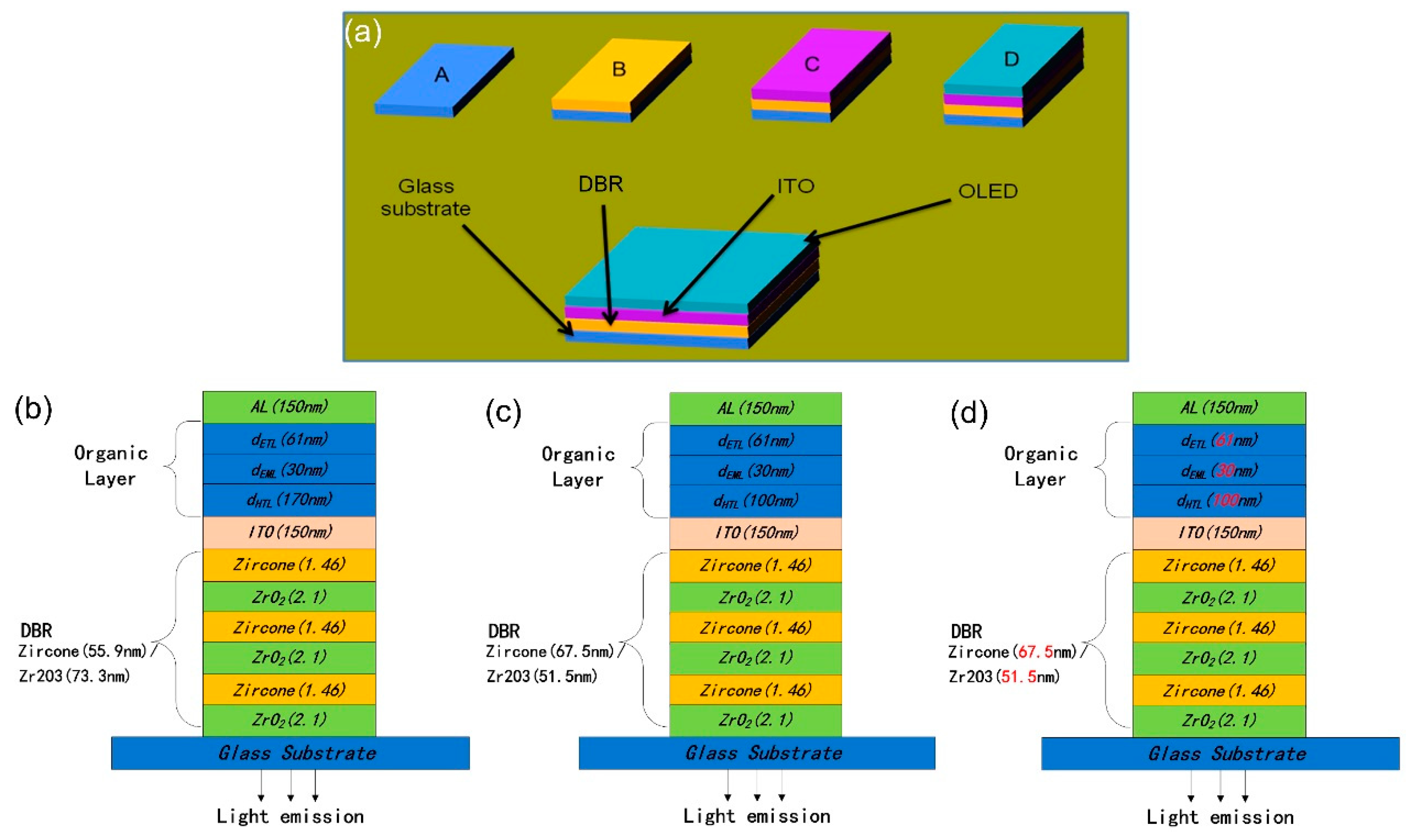
2.1. Design of DBR for OLEDs

Zirconium oxide (ZrO2) and zircone were used as the bottom dielectric mirror for the DBR structure. In OLED devices, molybdenum oxide (MoO3) and 1,4-bis[N-(1-naphthyl)-N0-phenylamino]-4,4′ diamine (NPB) are employed as hole injection layers (HIL); 4,4′,4″-tris-(N-carbazolyl)-triphenylamine (TCTA) is employed as a hole transport layer (HTL); lithium fluoride (LiF) is the electron injection layer (EIL); tris(8-hydroxyquinoline) aluminum (Alq3) and 1,3,5-tris(2N-phenylbenzimidazolyl)benzene (TPBi) are electron transport layers (ETL). The emitting layer (EML) in Device A is composed of two emission components: TCTA doped with 10 wt% of fac-tris(2-phenylpyridine) iridium (Ir(ppy)3) acts as a green-emitting material layer (EML), while 3 wt% 1-4-Di-[4-(N,N-diphenyl)amino]styryl-benzene (DSA-Ph)-doped 4,4′-bis(N-carbazolyl)biphenyl (CBP) acts as a blue EML.
Figure 1 displays the schematic structure of the device with the DBR. In OLEDs, a metal cathode and dielectric mirror were formed together on the glass substrate, which defined the microcavity structure. The aluminum (Al) metal layer and six pairs of the ZrO2/zircone stack were used as cathode and DBR layers. A classical calculation was performed to estimate the dielectric mirror regarding its reflectivity through refractive indices. In Figure 1, the numbers in parentheses after zircone (1.46) and ZrO2 (2.1) are refractive indices. The light generated in OLEDs was emitted through the dielectric mirror as well as the glass substrate. The equation below helped to calculate the forward theoretic emission spectrum considering the classical optics [19].
E c a v ( λ ) 2 = ( 1 R d ) [ 1 + R m + 2 R m 0.5 cos ( 4 π x λ ) ] 1 + R d R m 2 ( R d R m ) 0.5 cos ( 4 π L λ ) E n ( λ ) 2
where λ denotes the wavelength of emission, x denotes the emitting layer’s effective distance between the metal mirror, and indium–tin oxide (ITO) substrate, Rm represents the reflectivity exhibited by the metal mirror, and Rd represents the reflectivity exhibited by the dielectric mirror. L denotes the overall optical length exhibited by the microcavity OLED device. En(λ) denotes the original spectrum. The below equation expresses L considering the classical optics [20].
L = λ 2 ( n e f f Δ n ) + i n i d i + | φ m 4 π λ |
where neff stands for the essential index of refraction, Δn stands for the difference in the index of refraction between the two layers of the dielectric mirror, di stands for the thickness, and ni stands for the index of refraction exhibited by the organic layers as well as ITO. Φm refers to the change in phase at the metal mirror. The relationship = 2L(λ) expresses the cavity mode, where m denotes the index of the mode, where the adjustment can be performed via changing the length of the cavity, i.e., L(λ).

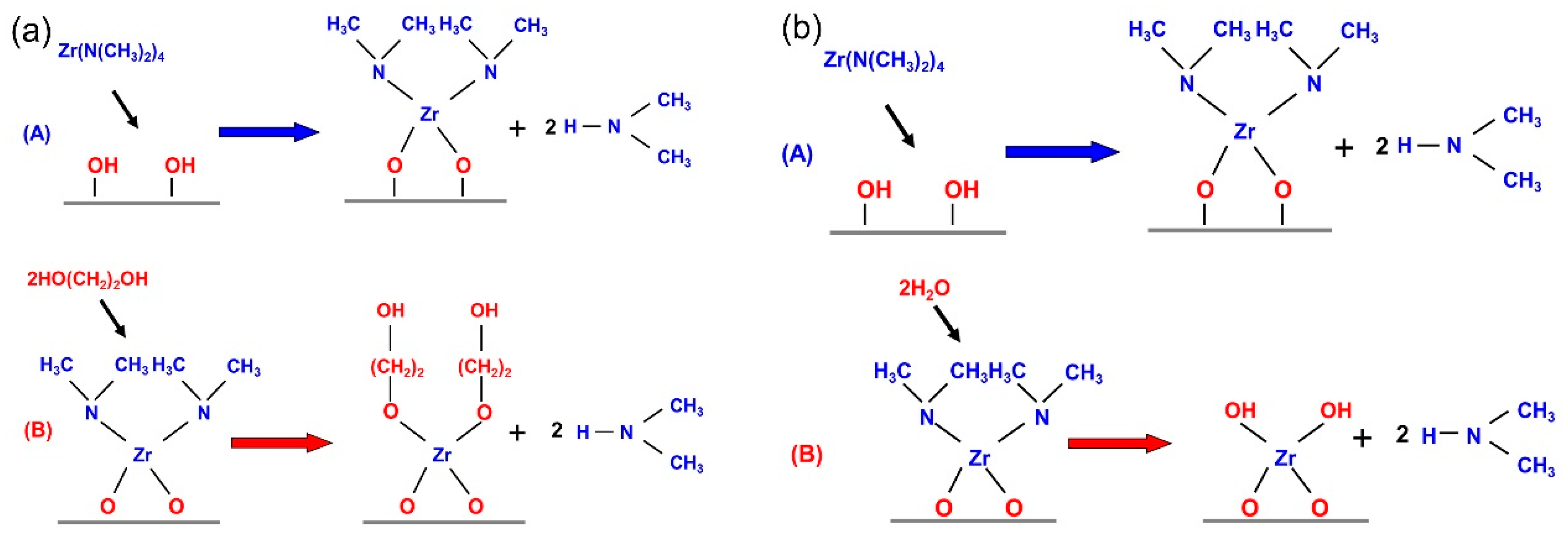
2.2. ALD ZrO2/Zircone DBR Structure

The DBR ZrO2/zircone films were deposited in the Beneq TFS-200 ALD reactor, which has been explained in another work [21]. Firstly, the sonication was conducted to clean the glass substrate, which was then put in detergent solution as well as deionized water in succession and then treated by UV ozone. Zircone films were manufactured via etrakis (dimethylamido) (TDMAZ) as well as ethylene glycol (EG) as the precursors at 100 °C. The ZrO2 film was deposited at 150 °C, taking H2O as well as TDMAZ as precursors. The experiment took nitrogen (N2, 99.999%) as the purging gas and the carrier. The ALD process was performed under a pressure of 600 mTorr. Zircone films underwent deposition with a TDMAZ pulse of 200 ms, an EG pulse of 100 ms, and a purge time of 15 s, and ALD ZrO2 films underwent deposition with a TDMAZ pulse of 200 ms, an N2 purge of 15 s, and an H2O flow of 250 ms with 20 s N2 purging. Figure 2 displays the common reaction process between the metal alkyl and diol of ALD-fabricated film.

2.3. DBR Based OLED Fabrication

The organic materials and Al cathode received traditional vacuum deposition under a basic pressure of less than 7 × 10⁻⁶ Pa, thereby fabricating devices A, B, and C. The quartz crystal monitor helped to control the thickness of the film layer in situ. The three device structures are shown below.
Device A: ITO (150 nm)/MoO3 (80 nm)/MoO3: 50 wt% TCTA (50 nm)/TCTA (40 nm)/TCTA: 10 wt% Ir(ppy)3 (30 nm)/TPBi (60 nm)/Liq (0.3 nm)/Al (150 nm)
Device B: ITO (150 nm)/MoO3 (20 nm)/NPB (50 nm)/CPB: 3 wt% DSA-Ph (30 nm)/Alq3 (60 nm)/Liq (1 nm)/Al (150 nm)
Device C: ITO (150 nm)/NPB (45 nm)/TCTA (5 nm)/CBP: 2 wt% (bt)2Ir(acac) (2 nm)/CBP (4 nm)/CBP: 2 wt% BmPAC (4 nm)/CBP (4 nm)/TPBi: 2 wt% BmPAC (2 nm)/TPBi (2 nm)/TPBi: 2 wt% C545T (4 nm)/TPBi (2 nm)/TPBi: 5 wt% PQIr (4 nm)/TPBi (25 nm)/LiF (0.3 nm)/Al (150 nm)
Six pairs of ZrO2/zircone films were deposited on the glass substrates with ALD, and then the ITO layer was sputtered. We set the ZrO2 and zircone layer thicknesses as equal to the quarter length of the optical exhibited by a central wavelength. ZrO2 and Zircone layers had thicknesses of 55.9 nm and 73.3 nm, 51.5 nm and 67.5 nm, and 55.9 nm and 73.3 nm for Devices A, B, and C, respectively. We cleaned the prepared substrate using detergent, deionized water, acetone, and isopropanol, respectively. After a 15-min treatment with UV-zone, the substrates were loaded into a specific chamber with high vacuum heat evaporation. The organic layers were deposited under a pressure lower than 7 × 10⁻⁶ mbar. Shadow masks helped to successfully evaporate the patterned organic layer as well as the metal cathode layer. The deposition of the whole organic layers, MoOx, as well as the Al cathode, occurred without exposure to the air, by which OLEDs with active areas of 4(2 × 2) mm2 were obtained. The deposition rates for organic materials MoOx and Al were 1.0 Å s−1, 0.3 Å s−1, and 5.0 Å s−1, respectively.
Atomic force microscopy (AFM) (Nanonavi SPA-400SPM) helped to analyze the surface morphological images exhibited by DBR films. A spectrophotometer(U-3900H, Hitachi, Japan) helped to measure the reflectance under normal conditions. The HI-TACHI F-4500 florescence spectrophotometer recorded the photoluminescence spectra. A Keithley 2400 source meter together with a PR650 luminance color meter helped to measure the current, voltage, and luminescence features. The measurement of the spectra and luminance exhibited by each device was performed directly perpendicular to the substrate.

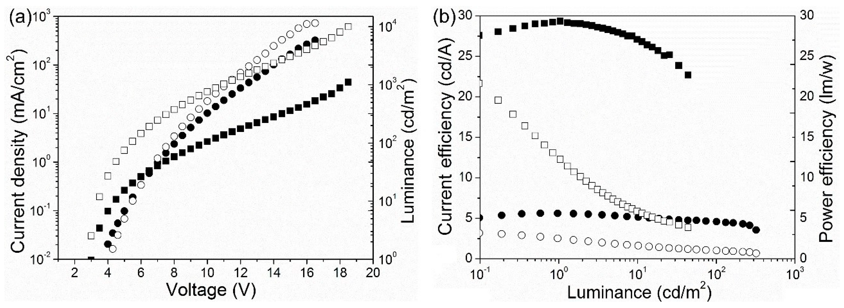
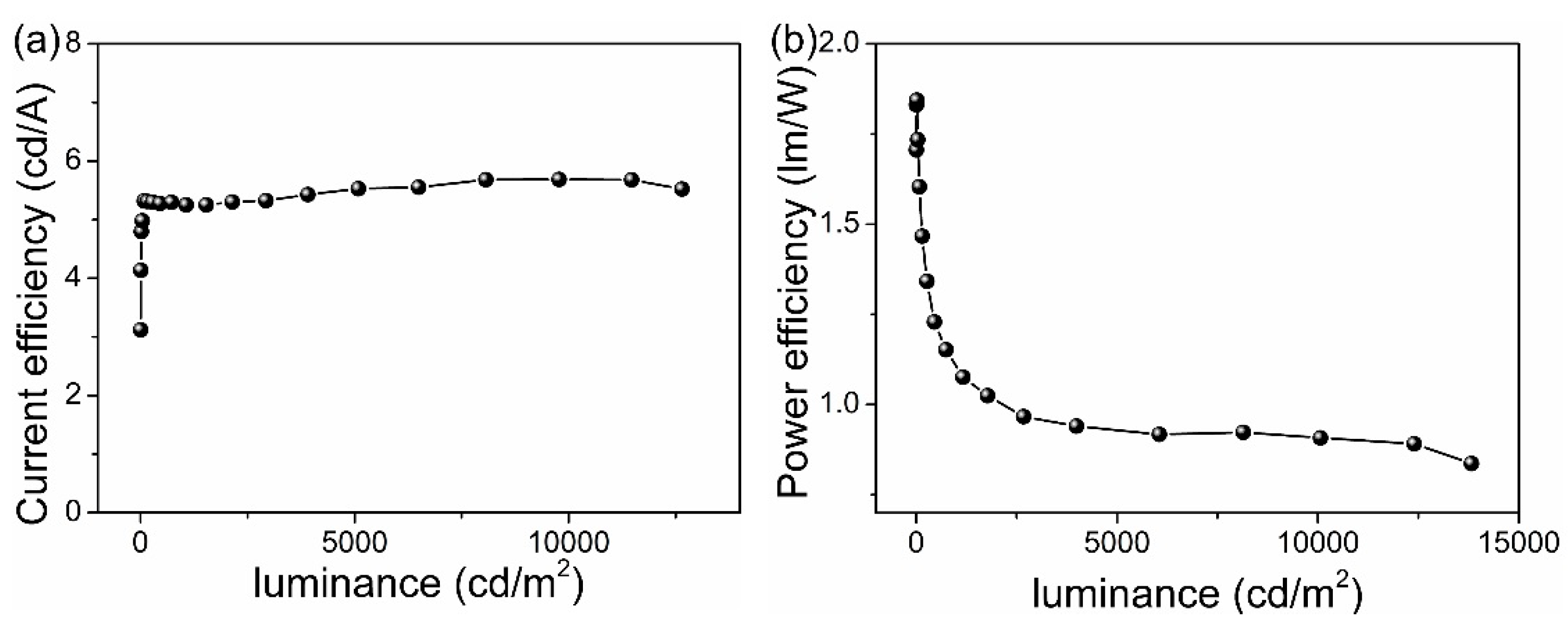
3. Results and Discussion

The J–V–L features of device A and device B are displayed in Figure 3a. The turn-on voltage (Von) of device B (2.6 V) appeared to be lower than that of device A (2.8 V). This means that there is a best match in the energy level between the highest occupied molecular orbital (HOMO) and lowest unoccupied molecular orbital (LUMO) of every organic layer for device A. [22] Meanwhile, the current density as well as luminance of device B rose more sharply with the increase in voltage compared with device A. Device A exhibited the largest CE and PE, which were 29.4 cd A−1 and 21.5 lm W−1, respectively. Besides, the CE and PE were 6.1 cd A−1 and 2.6 lm W−1 for device B.
We also fabricated multi-emissive layer WOLEDs (Device C), and Figure 4 displays the corresponding PE and CE. Device C reveals a high CE value of 5.3 cd A−1 at the 100 cd m−2 or of 5.4 cd A−1 at the 1000 cd m−2 or of 5.7 cd A−1 at the 10,000 cd m−2 and a turn-on voltage of 5.5 V compared with device A. Device C uses NPB as the HIL, but device A and device B use MoOx as the HIL. If NPB shows a deeper HOMO level (5.6 eV), it is more difficult to inject a hole in device C in comparison to device A and B. The weak hole injection is likely to cause both a high turn-on voltage and an imbalance between electron as well as hole carriers. [23] Simultaneously, the large number of multiple EMLs as well as the interlayer of the device C cause a stronger electric field, of which luminance is the same as that of other devices, which also leads to the lower efficiency of device C. In particular, these three devices all show a relatively low roll-off in CE with increasing luminance. The host materials, of which the triplet energy levels are higher compared with emitters, are used as the interlayers in different devices. These interlayers function as confining triplet excitons exhibited by dopants in emissive layers on the one hand and explore the recombined zone for electron and hole on the other hand. Therefore, the low efficiency roll-off characteristics of the devices are attributed to the introduction of interlayers [24].
AFM was measured to thoroughly study the surface morphology of a DBR layer with a tapping mode, and the result is shown in Figure 5. The DBR structure exhibited a root mean square (RMS) surface roughness of 2.31 nm, suggesting that the films have a lower peak defeat, which is beneficial for subsequent film preparation. Obviously, it seems that the peak defeat and high surface roughness can damage the emission layers. The uniform film of DBR layers with low surface roughness is also favorable for improving the device performance.
The reflectance spectrum of the DBR ZrO2/zircone films is shown in Figure 6, together with the reference device without a DBR structure using the same configuration as Device A. Obviously, DBR layers exhibit very high reflectivity, especially for the green region, with a reflectivity of up to 90%. The DBR structure also has a stop band, which is broad enough to confine the whole EL emission in addition to the wavelength of cavity resonance. According to these results, it is convincing that the ALD method can effectively and precisely control the thickness to improve the reflectivity of DBRs in comparison with other film deposition methods, such as sputtering or electron beam evaporation.
The normalized EL spectra of device A and device B with the DBR microcavity are displayed in Figure 7. The EL spectrum of the reference device without a DBR structure demonstrates a spectrally broad emission at the peak of 512 nm, and the full-width at half-maximum (FWHM) reaches 65 nm (Figure 5). After depositing the DBR structure, based on the modeled EL spectrum for Device A, one cavity mode lies at 500 nm (FWHM 13 nm) and another lies at 588 nm (FWHM 16 nm) (Figure 7a). The modeled EL emission shows the coordinates of (0.37, 0.48), which is within that of a warm white color. To optimize the luminance from the perspective of design, the antinodes of the confined cavity field, at 500 and 588 nm, respectively, are placed near the interface between the NPB layer and Alq3 layer, and excitons come into being around the interface [25,26]. Additionally, Device B also exhibits a very narrow EL spectrum with three emission peaks (Figure 7b).
More importantly, with the application of driving voltage, we can see the white light along the normal direction from the side of the glass. Figure 7a displays the EL spectrum at the range of 5–13 V in a normal direction. The emission color remains stable, although the voltages change due to the simple structure and single emitting layer. Therefore, the recombination zone hardly changes with increasing voltage [27]. With the increase in the operation voltage, the resonator mode in the microcavity does not change. Thus, the ratio of emission intensity with respect to the inherent emission changes little, resulting in a good chromatic stability [28]. The CIE coordinates exhibited by device A shows a negligible slight variation of (±0.01, ±0.01). Furthermore, Device C also yields a high color purity white emission when the luminance changes between 100 cd m−2 and 10,000 cd m−2, and there are four resonant peaks of 420 nm, 488 nm, 552 nm, and 620 nm (Figure 8).

4. Conclusions

In conclusion, high-performance WOLEDs have been successfully made using the ALD fabricated microcavity structure to enhance the intensity of emission as well as to narrow the spectra in OLEDs at the same time. According to the result, the DBR structure helped to greatly modify the spectra as well as the intensity. The results indicate that the DBR layers can remarkably adjust the emission of OLEDs. Based on the DBR structure, a high CE of 29.4 cd A−1 and low Von of 2.6 V is demonstrated with narrowed FWHM and superb color stability over the working voltage of 5–13 V. The four-peak WOLED also yields a high color purity white emission when the luminance changes between 100 and 10,000 cd m−2. From the viewpoint of commercial application, on the one hand, improving the strong color purity and, on the other hand, enhancing the intensity contribute to the attractive practical applications of WOLEDs in high-definition displays and lighting sources. Additionally, it is expected that this work will provide a new insight in achieving high-performance WOLEDs with a DBR structure fabricated by ALD.

Author Contributions

Data Curation, S.W. and Z.L.; Funding Acquisition, H.Z.; Investigation, Y.W. and J.Y.; Supervision, B.W.; Writing—Original Draft, Y.W. and J.Y.; Writing—Review & Editing, H.Z.

Funding

Support by the Natural Science Foundation of Fujian Province (2018J0164, 2017H0004) and the Foundation of Fujian Jiangxia University (JXZ2016003).

Conflicts of Interest

The authors declare no conflict of interest.

References

  1. Miao, Y.Q.; Tao, P.; Wang, K.X.; Li, H.X.; Zhao, B.; Gao, L.; Wang, H.; Xu, B.; Zhao, Q. Highly efficient red and white organic light-emitting diodes with external quantum efficiency beyond 20% by employing pyridylimidazole-based metallophosphors. ACS Appl. Mater. Interfaces 2017, 9, 37873–37882. [Google Scholar] [CrossRef] [PubMed]
  2. Bui, T.T.; Goubard, F.; Ibrahim-Ouali, M.; Gigmes, D.; Dumur, F. Thermally activated delayed fluorescence emitters for deep blue organic light emitting diodes: A review of recent advances. Appl. Sci. 2018, 8, 494. [Google Scholar] [CrossRef]
  3. Wang, S.; Yang, J.; Xu, T.; Dou, D.; Tang, Z.; Gao, Z.; Chen, M.; Guo, K.; Yu, J.; Plain, J.; et al. Highly efficient and foldable top-emission organic light-emitting diodes based on Ag-nanoparticles modified graphite electrode. Org. Electron. 2019, 64, 146–153. [Google Scholar] [CrossRef]
  4. Wang, S.; Qiao, M.; Ye, Z.; Dou, D.; Chen, M.; Peng, Y.; Shi, Y.; Yang, X.; Cui, L.; Li, J.; et al. Efficient deep-blue electrofluorescence with an external quantum efficiency beyond 10%. iScience 2018, 9, 532–541. [Google Scholar] [CrossRef]
  5. D’Andrade, B.W.; Forrest, S.R. White organic light-emitting devices for solid-state lighting. Adv. Mater. 2004, 16, 1585–1595. [Google Scholar] [CrossRef]
  6. Wang, S.M.; Zhao, L.; Zhang, B.H.; Ding, J.Q.; Xie, Z.Y.; Wang, L.X.; Wong, W.Y. High-energy-level blue phosphor for solution-processed white organic light-emitting diodes with efficiency comparable to fluorescent tubes. iScience 2018, 6, 128–137. [Google Scholar] [CrossRef] [PubMed]
  7. Miao, Y.; Wang, K.; Zhao, B.; Gao, L.; Tao, P.; Liu, X.; Hao, Y.; Wang, H.; Xu, B.; Zhu, F. High-efficiency/CRI/color stability warm white organic light-emitting diodes by incorporating ultrathin phosphorescence layers in a blue fluorescence layer. Nanophotonics 2018, 7, 295–304. [Google Scholar] [CrossRef] [Green Version]
  8. Lee, J.; Cho, H.; Koh, T.W.; Hofmann, S.; Kim, Y.H.; Yun, C.; Schwab, T.; Reineke, S.; Lüssem, B.; Lee, J.I.; et al. Straight-forward control of the degree of micro-cavity effects in organic light-emitting diodes based on a thin striped metal layer. Org. Electron. 2013, 14, 2444–2450. [Google Scholar] [CrossRef]
  9. Melpignano, P.; Cioarec, C.; Clergereaux, R.; Gherardi, N.; Villeneuve, C.; Datas, L. E-beam deposited ultra-smooth silver thin film on glass with different nucleation layers: An optimization study for OLED micro-cavity application. Org. Electron. 2010, 11, 1111–1119. [Google Scholar] [CrossRef]
  10. Schwab, T.; Schubert, S.; Müller-Meskamp, L.; Leo, K.; Gather, M.C. Eliminating micro-cavity effects in white top-emitting OLEDs by ultra-thin metallic top electrodes. Adv. Opt. Mater 2013, 1, 921–925. [Google Scholar] [CrossRef]
  11. Zhou, G.J.; Wong, W.Y.; Yao, B.; Xie, Z.Y.; Wang, L.X. Triphenylamine-dendronized pure red iridium phosphors with superior OLED efficiency/color purity trade-offs. Angew. Chem. 2007, 119, 1167–1169. [Google Scholar] [CrossRef]
  12. Xu, K.; Lu, C.; Huang, Y.; Hu, J.; Wang, X. Enhanced outcoupling efficiency and removal of the microcavity effect in top-emitting OLED by using a simple vapor treated corrugated film. RSC Adv. 2017, 7, 54876–54880. [Google Scholar] [CrossRef] [Green Version]
  13. Park, M.J.; Kim, S.K.; Pode, R.; Kwon, J.H. Low absorption semi-transparent cathode for micro-cavity top-emitting organic light emitting diodes. Org. Electron. 2018, 52, 153–158. [Google Scholar] [CrossRef]
  14. Al-Asbahi, B. Influence of SiO2/TiO2 nanocomposite on the optoelectronic properties of PFO/MEH-PPV-based OLED devices. Polymers 2018, 10, 800. [Google Scholar] [CrossRef]
  15. Lei, P.H.; Wang, S.H.; Juang, F.S.; Tseng, Y.H.; Chung, M.J. Effect of SiO2/Si3N4 dielectric distributed Bragg reflectors (DDBRs) for Alq3/NPB thin-film resonant cavity organic light emitting diodes. Opt. Commun. 2010, 283, 1933–1937. [Google Scholar] [CrossRef]
  16. Zaera, F. The surface chemistry of atomic layer depositions of solid thin films. J. Phys. Chem. Lett. 2012, 3, 1301–1309. [Google Scholar] [CrossRef]
  17. Tseng, M.H.; Yu, H.H.; Chou, K.Y.; Jou, J.H.; Lin, K.L.; Wang, C.C.; Tsai, F.Y. Low-temperature gas-barrier films by atomic layer deposition for encapsulating organic light-emitting diodes. Nanotechnology 2016, 27, 295706. [Google Scholar] [CrossRef]
  18. Jeong, E.G.; Han, Y.C.; Im, H.G.; Bae, B.S.; Choi, K.C. Highly reliable hybrid nano-stratified moisture barrier for encapsulating flexible OLEDs. Org. Electron. 2016, 33, 150–155. [Google Scholar] [CrossRef]
  19. Kim, S.Y.; Lee, J.H.; Lee, J.H.; Kim, J.J. High contrast flexible organic light emitting diodes under ambient light without sacrificing luminous efficiency. Org. Electron. 2012, 13, 826–832. [Google Scholar] [CrossRef]
  20. Tao, P.; Liang, H.; Xia, X.; Liu, Y.; Jiang, J.; Huang, H.; Feng, Q.; Shen, R.; Luo, Y.; Du, G. Enhanced output power of near-ultraviolet LEDs with AlGaN/GaN distributed Bragg reflectors on 6H-SiC by metal-organic chemical vapor deposition. Superlattices Microstruct. 2015, 85, 482–487. [Google Scholar] [CrossRef]
  21. Zhang, H.; Ding, H.; Wei, M.J.; Li, C.; Wei, B.; Zhang, J.H. Thin film encapsulation for organic light-emitting diodes using inorganic/organic hybrid layers by atomic layer deposition. Nanoscale Res. Lett. 2015, 10, 169. [Google Scholar] [CrossRef] [PubMed]
  22. Nozoe, S.; Matsuda, M. Enhanced emission by accumulated charges at organic/metal interfaces generated during the reverse bias of organic light emitting diodes. Appl. Sci. 2017, 7, 1045. [Google Scholar] [CrossRef]
  23. Ho, S.; Xiang, C.Y.; Liu, R.; Chopra, N.; Mathai, M.; So, F. Stable solution processed hole injection material for organic light-emitting diodes. Org. Electron. 2014, 15, 2513–2517. [Google Scholar] [CrossRef]
  24. Zheng, T.H.; Choy, W.C.; Ho, C.L.; Wong, W.Y. Improving efficiency roll-off in organic light emitting devices with a fluorescence-interlayer-phosphorescence emission architecture. Appl. Phys. Lett. 2009, 95, 264. [Google Scholar] [CrossRef]
  25. Ueda, H.; Takatsuka, Y.; Niinuma, Y.; Terada, R.; Kikuchi, A. Fabrication of NPB/Alq3 small-molecule multilayer structures with suppressed interface mixing by multi-jet mode electrospray deposition. Phys. Status Solidi (B) 2017, 254, 1600564. [Google Scholar] [CrossRef]
  26. Chiang, C.J.; Bull, S.; Winscom, C.; Monkman, A. A nano-indentation study of the reduced elastic modulus of Alq3 and NPB thin-film used in OLED devices. Org. Electron. 2010, 11, 450–455. [Google Scholar] [CrossRef]
  27. Kalinowski, J.; Palilis, L.C.; Kim, W.H.; Kafafi, Z.H. Determination of the width of the carrier recombination zone in organic light-emitting diodes. J. Appl. Phys. 2003, 94, 7764–7767. [Google Scholar] [CrossRef]
  28. Xiong, L.; Zhu, W.; Wei, N.; Li, J.; Sun, W.; Wu, X.; Cao, J.; Wang, Z. High color rendering index and chromatic-stable white organic light emitting diodes incorporating excimer and fluorescence emission. Org. Electron. 2013, 14, 32–37. [Google Scholar] [CrossRef]
Figure 1. (a) Process of organic light-emitting diode (OLED) device fabrication; (b) structure of green OLEDs; (c) structure of blue OLEDs, and (d) structure of white OLEDs (WOLEDs).
Applsci 09 01415 g001
Figure 2. A schematic diagram of the mechanism of reaction exhibited by distributed Bragg reflector (DBR) films of (a) the zircone layer and (b) the ZrO2 layer.
Applsci 09 01415 g002
Figure 3. (a) J–V curves (solid symbols) together with L–V curves (open symbols). (b) Current efficiency (CE) versus luminance (solid symbols), and power efficiency (PE) versus luminance (open symbols) for devices A and B. Squares show device A and circles show device B.
Applsci 09 01415 g003
Figure 4. (a) CE versus luminance and (b) PE versus luminance for device C.
Applsci 09 01415 g004
Figure 5. Tapping-mode atomic force microscopy (AFM) height images of the DBR film. The scan area of the image is 2 × 2 μm.
Applsci 09 01415 g005
Figure 6. The reflectance spectrum of the distributed Bragg reflector (DBR) and the electroluminescence (EL) spectrum of a reference device without a DBR structure with the same configuration as Device A.
Applsci 09 01415 g006
Figure 7. (a) EL spectrum of device A (inset is the corresponding CIE chromaticity coordinate). (b) EL spectrum of Device B.
Applsci 09 01415 g007
Figure 8. EL spectrum of device C (inset is the magnified first emission peak of the spectra).
Applsci 09 01415 g008

