Bin2Vec: A Better Wafer Bin Map Coloring Scheme for Comprehensible Visualization and Effective Bad Wafer Classification

Abstract
:1. Introduction
2. Literature Review
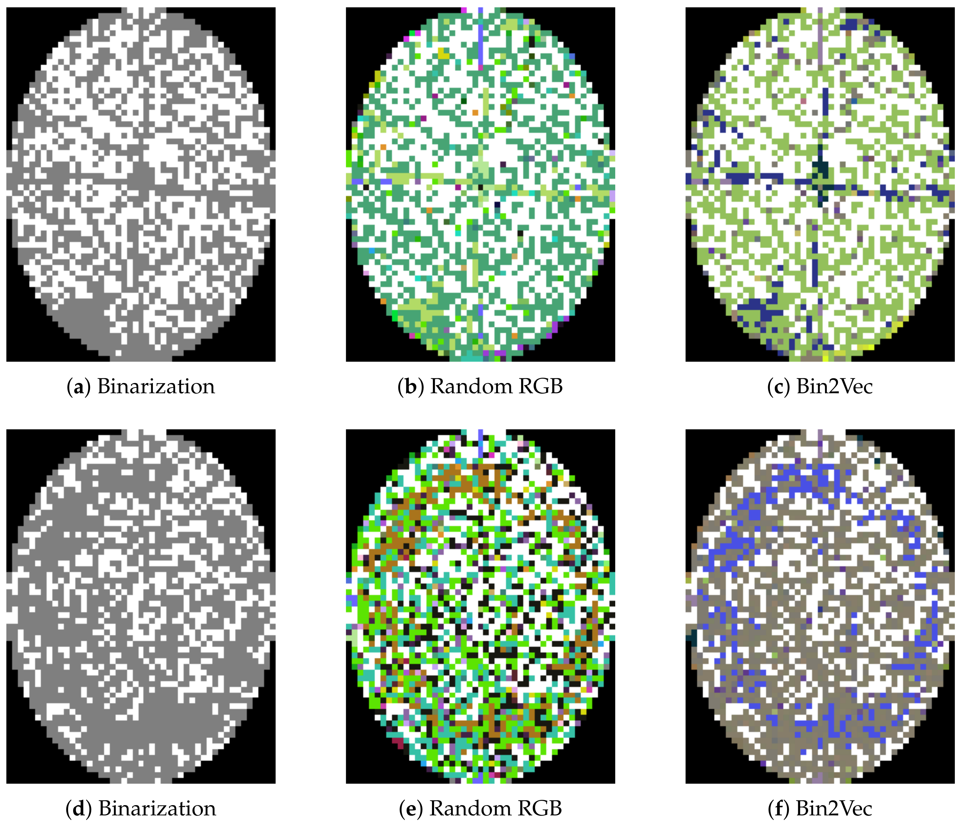
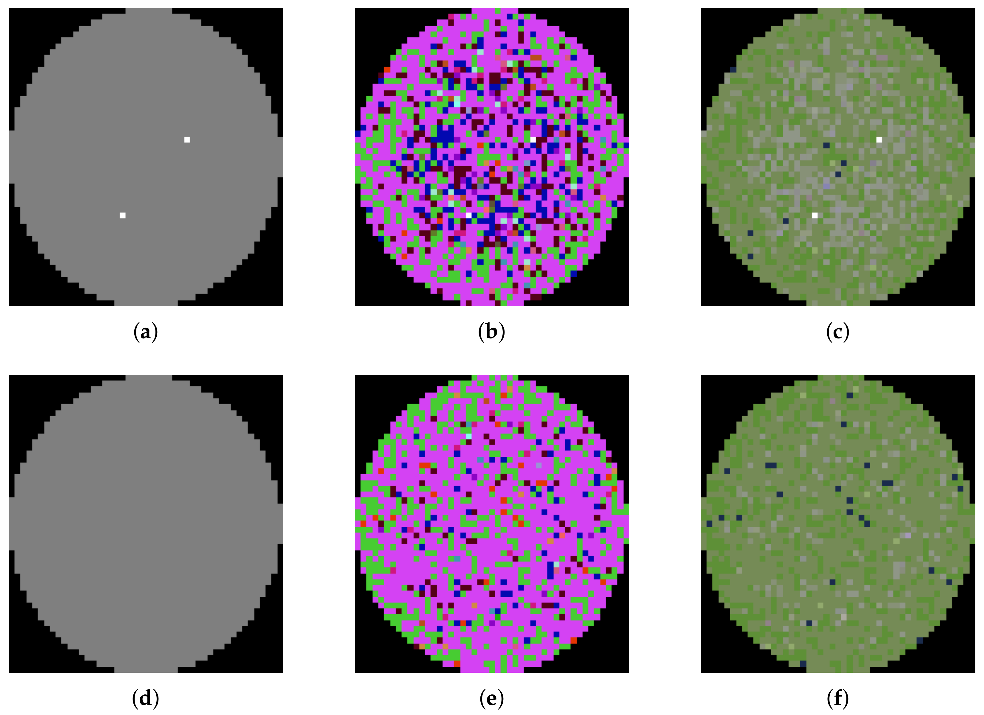
3. Bin2Vec: A Convolutional Neural Network-Based WBM Coloring Scheme
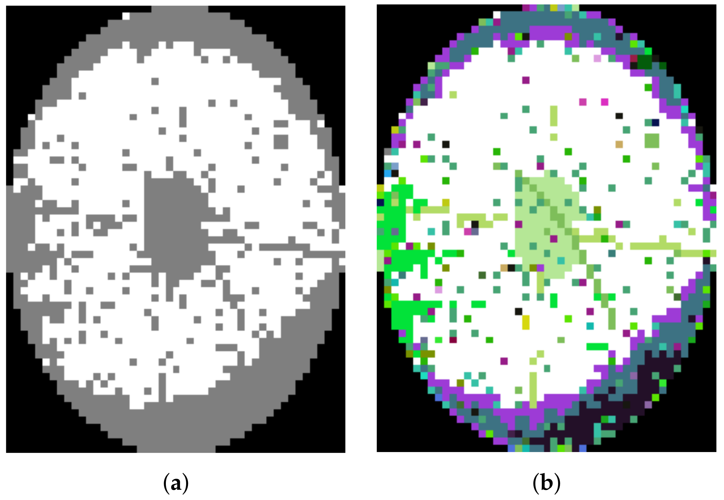
3.1. Data Description
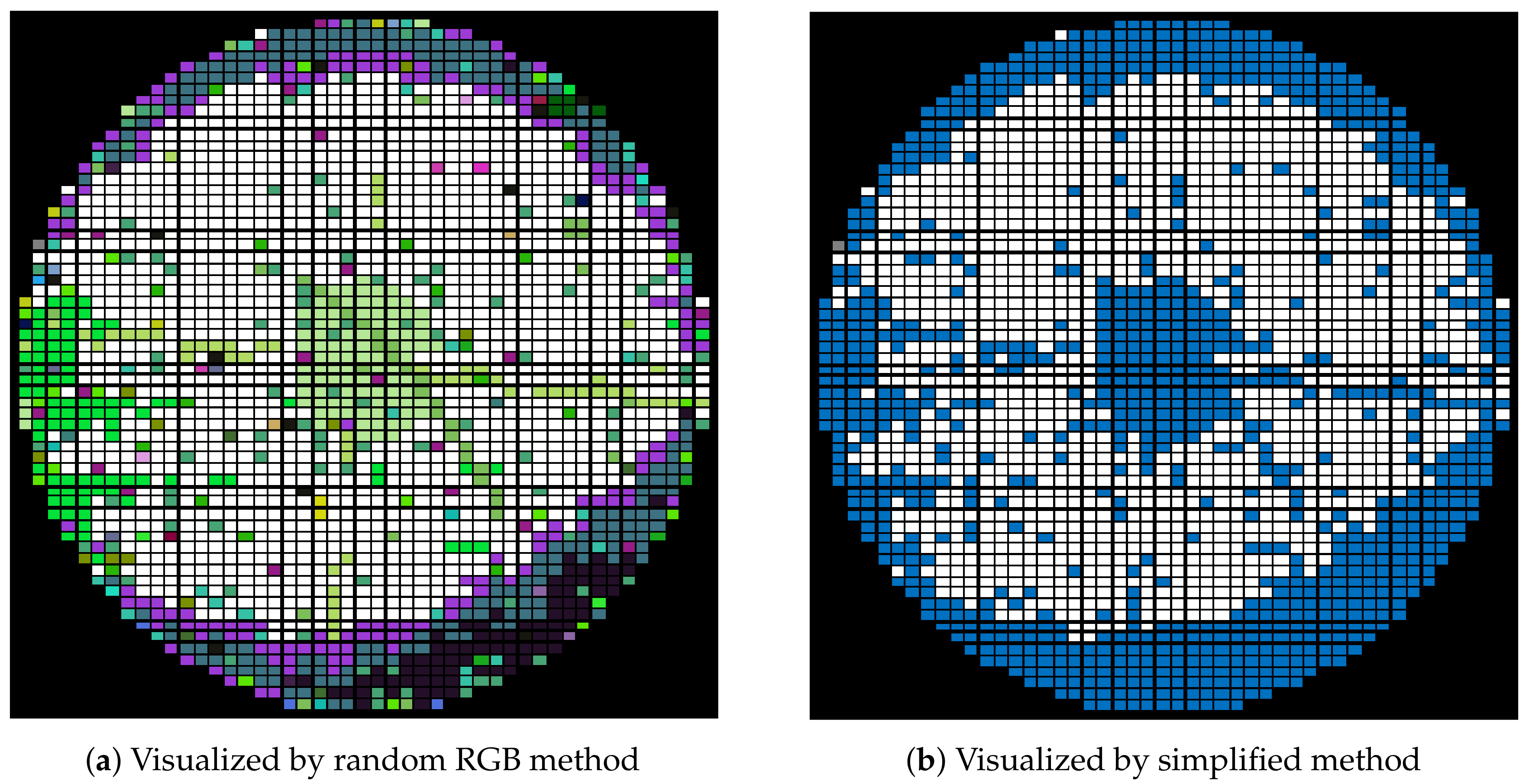
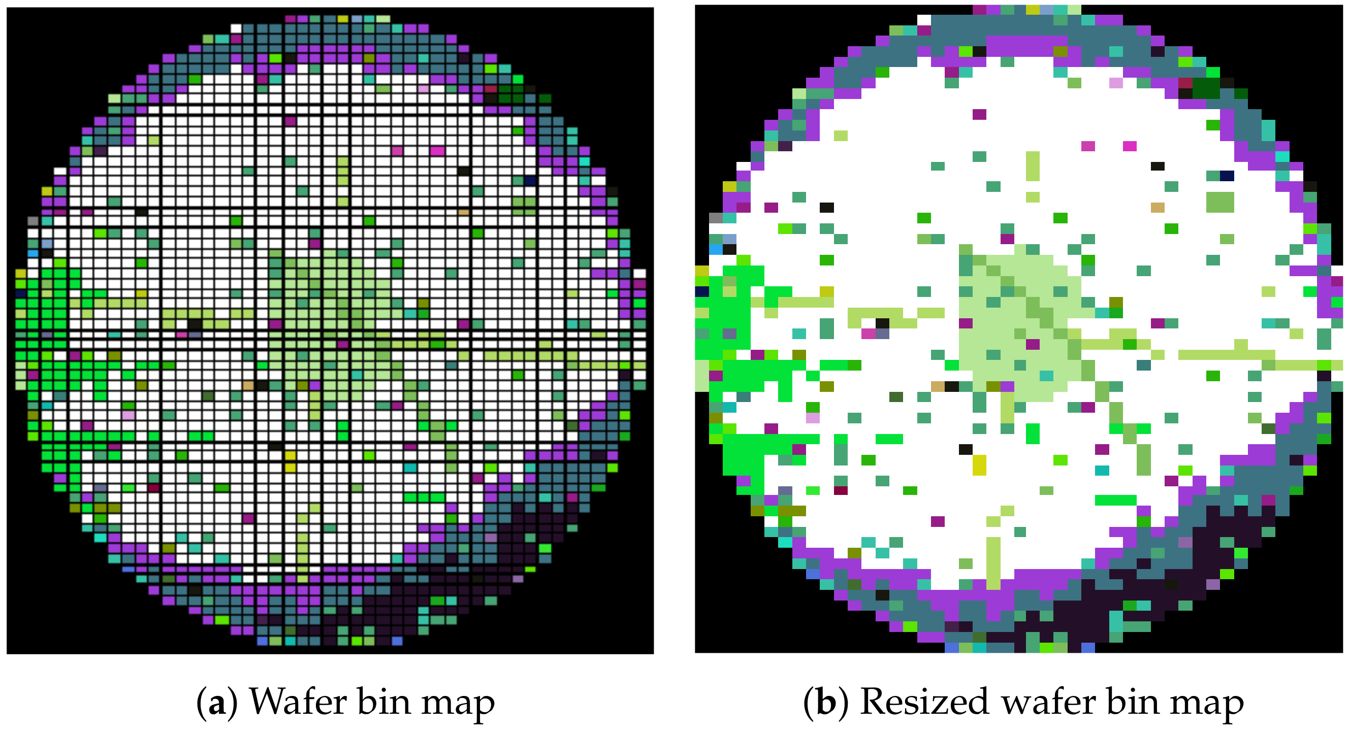
3.2. Word2Vec and Bin2Vec
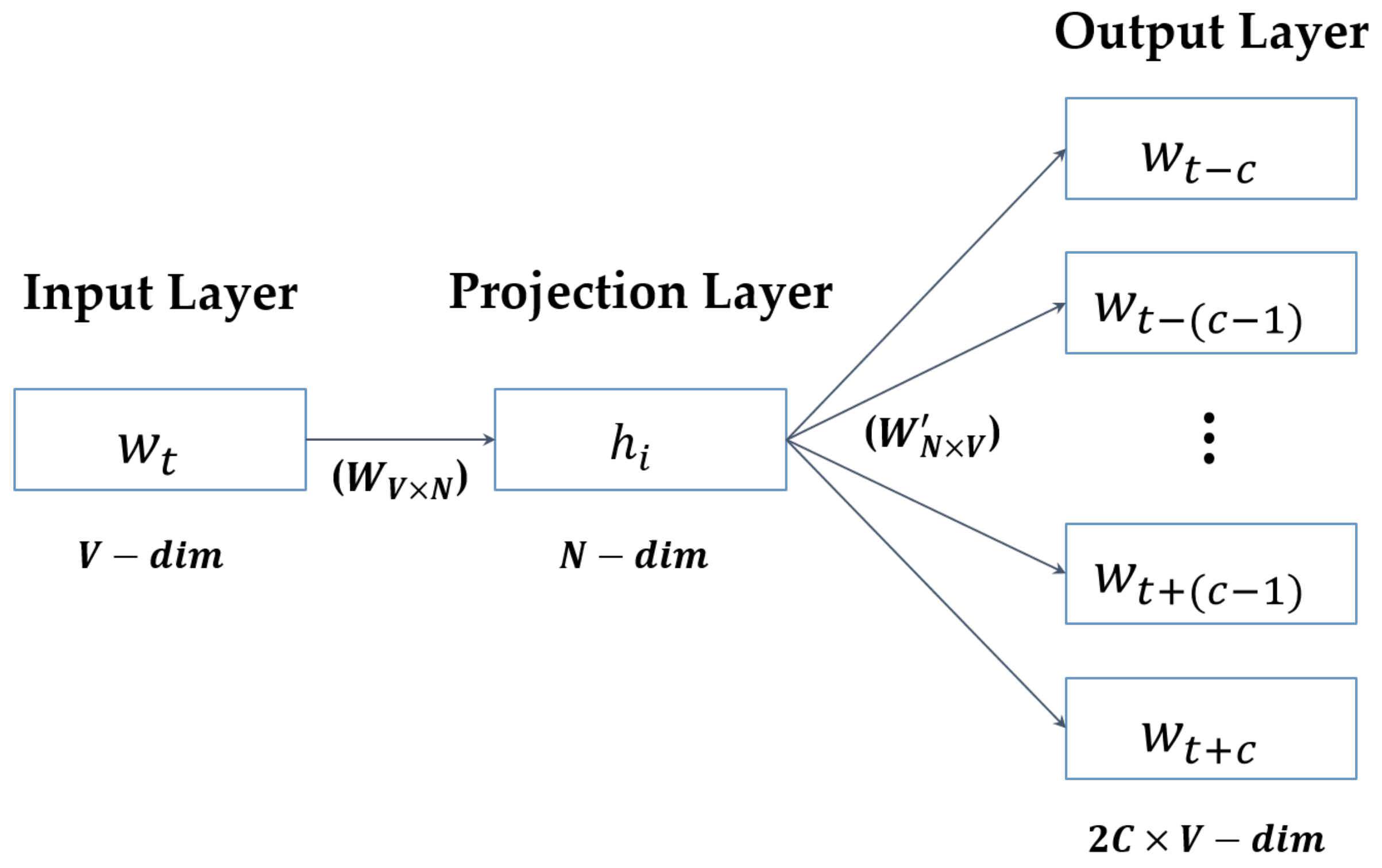
3.2.1. Word2Vec
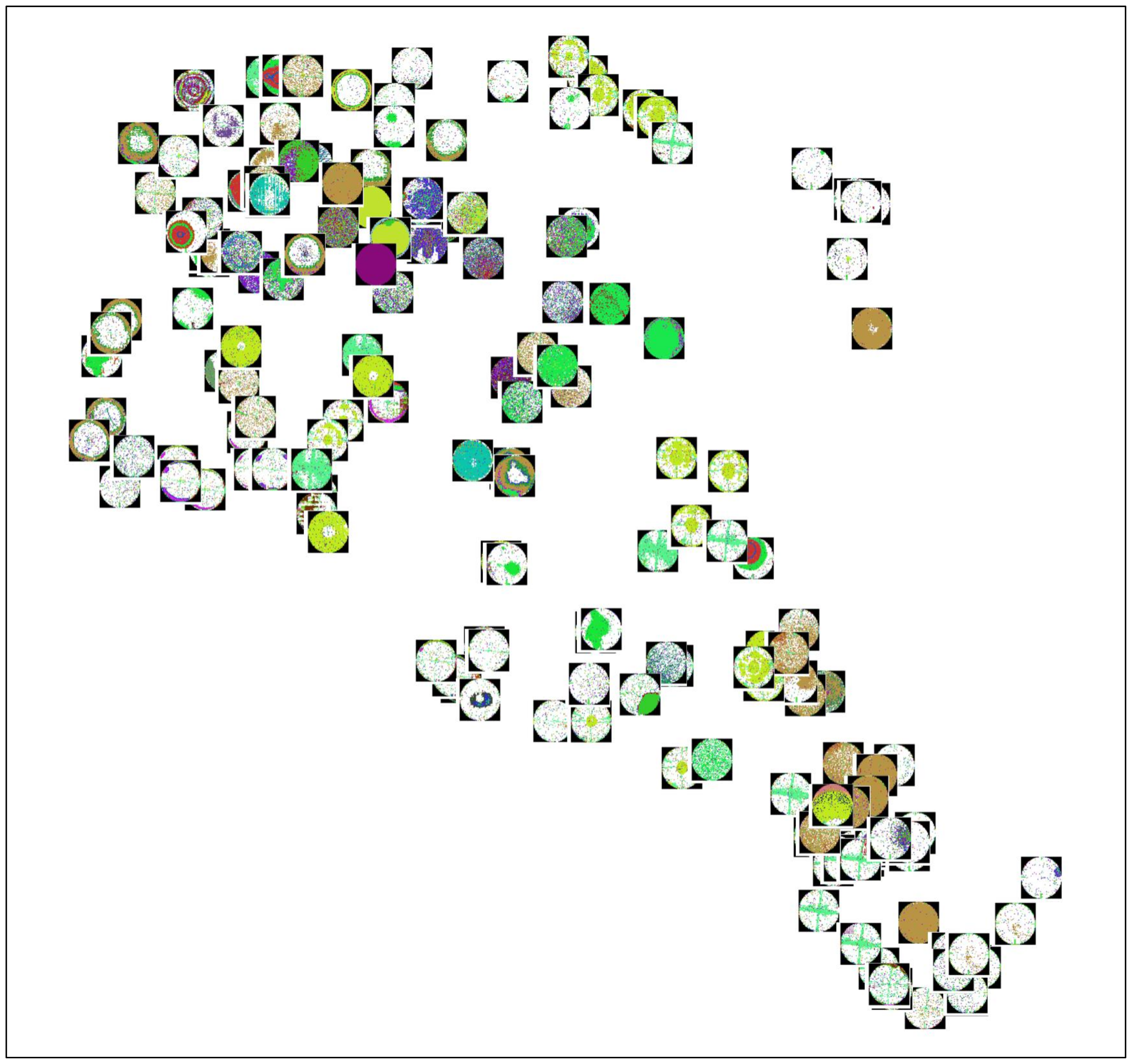
3.2.2. Bin2Vec
4. Experiment
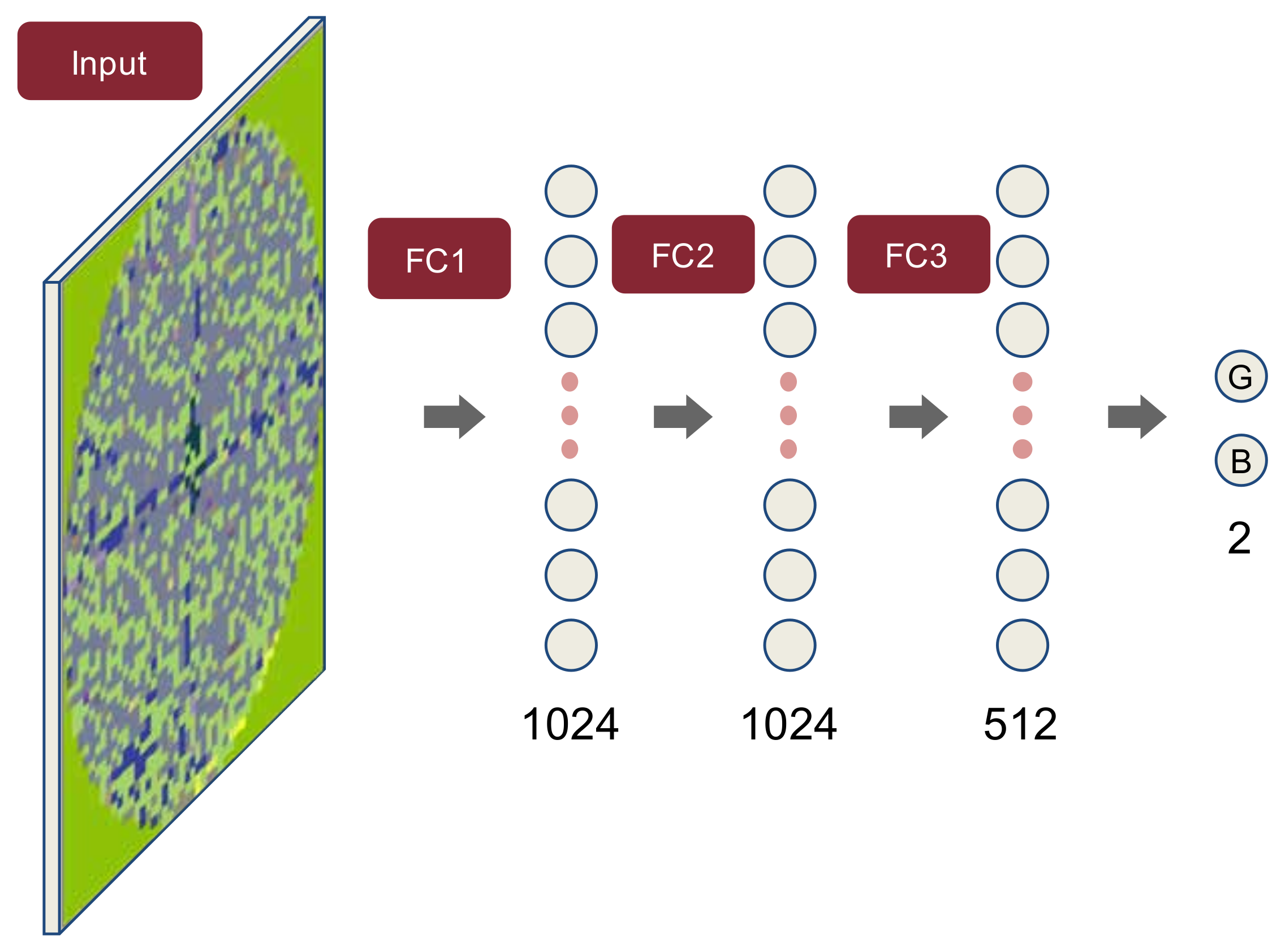
4.1. Convolution Neural Network
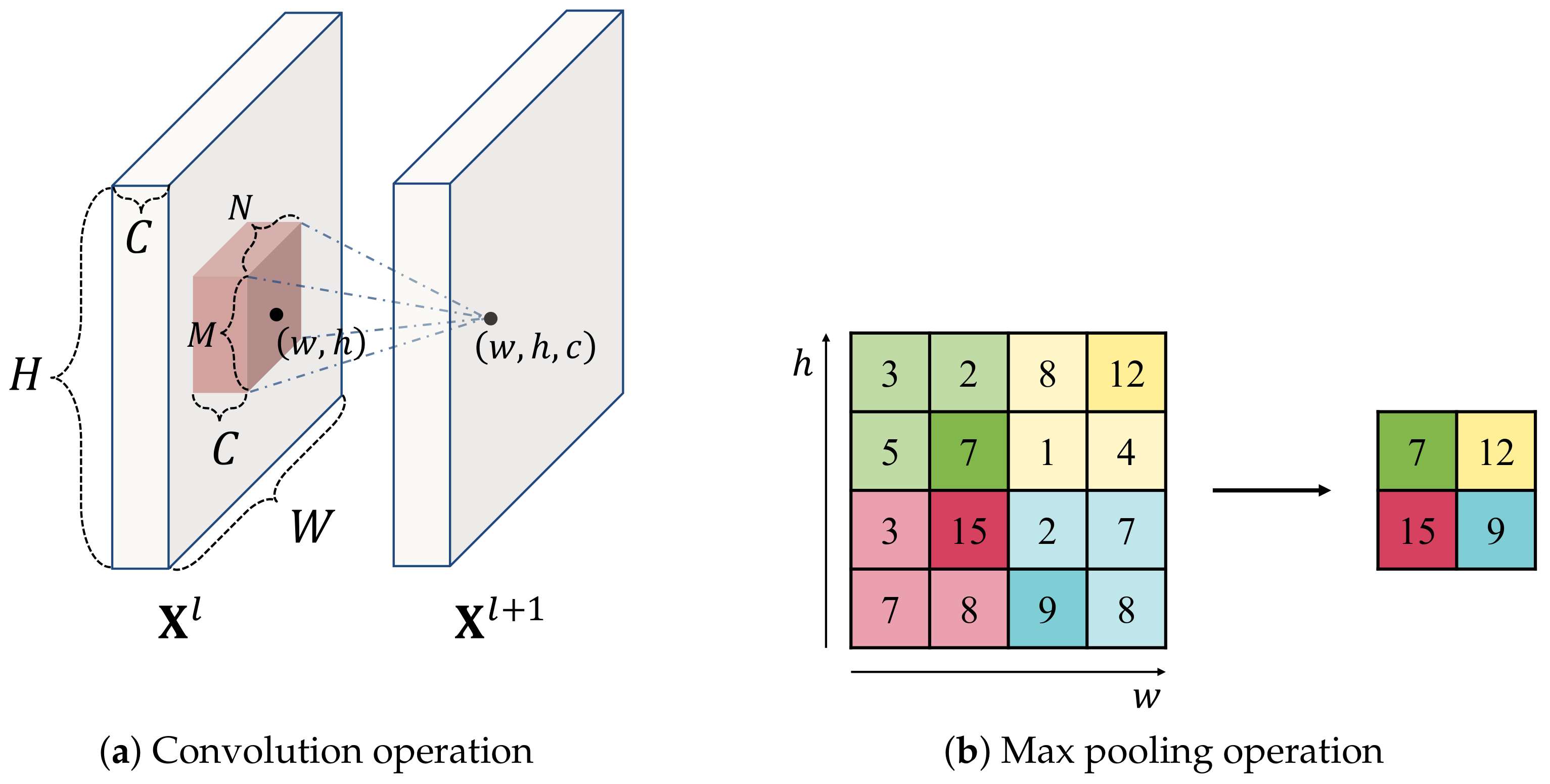
4.1.1. Convolution and Pooling Operation
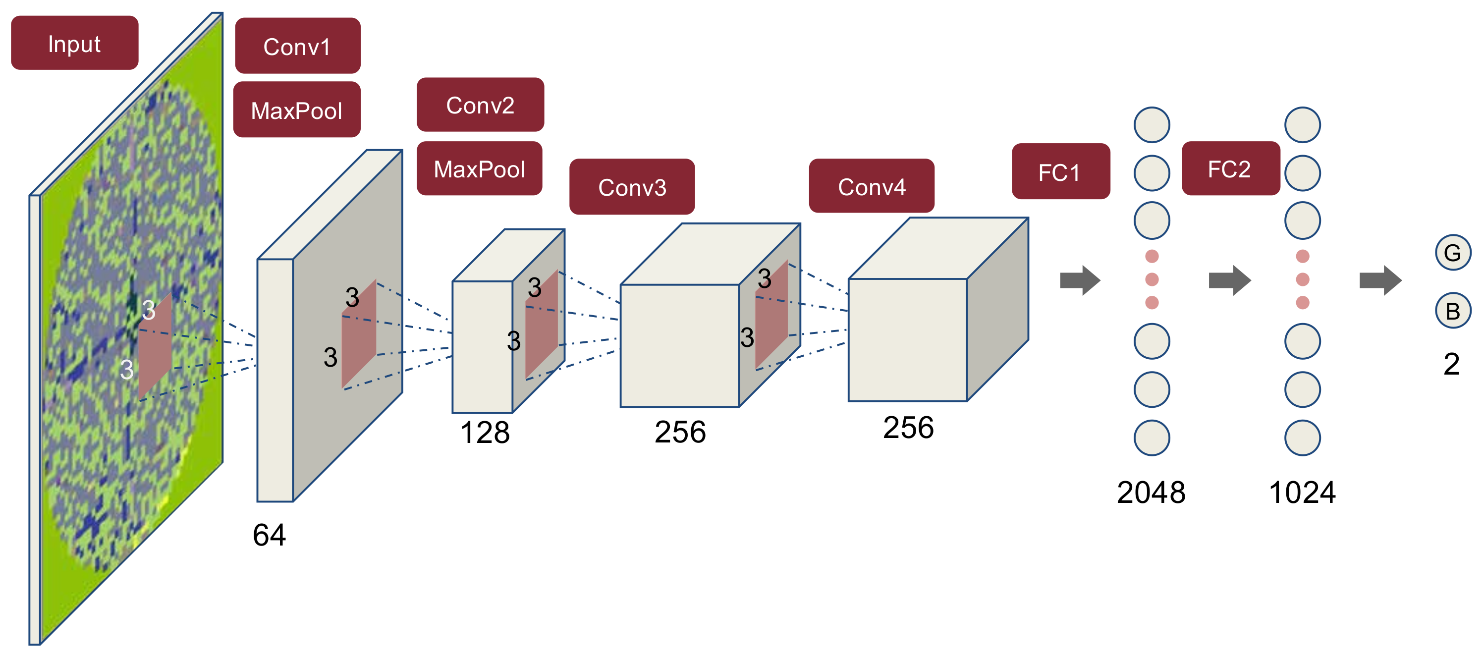
4.1.2. Convolutional Neural Network Architecture
4.2. Multilayer Perceptron
4.3. Random Forest
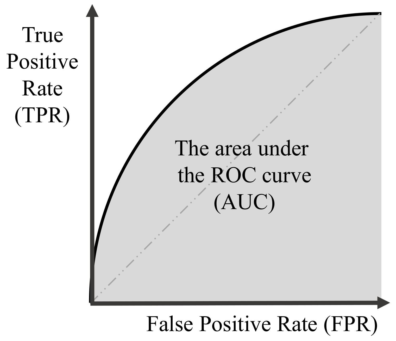
4.4. Performance Evaluation Criteria
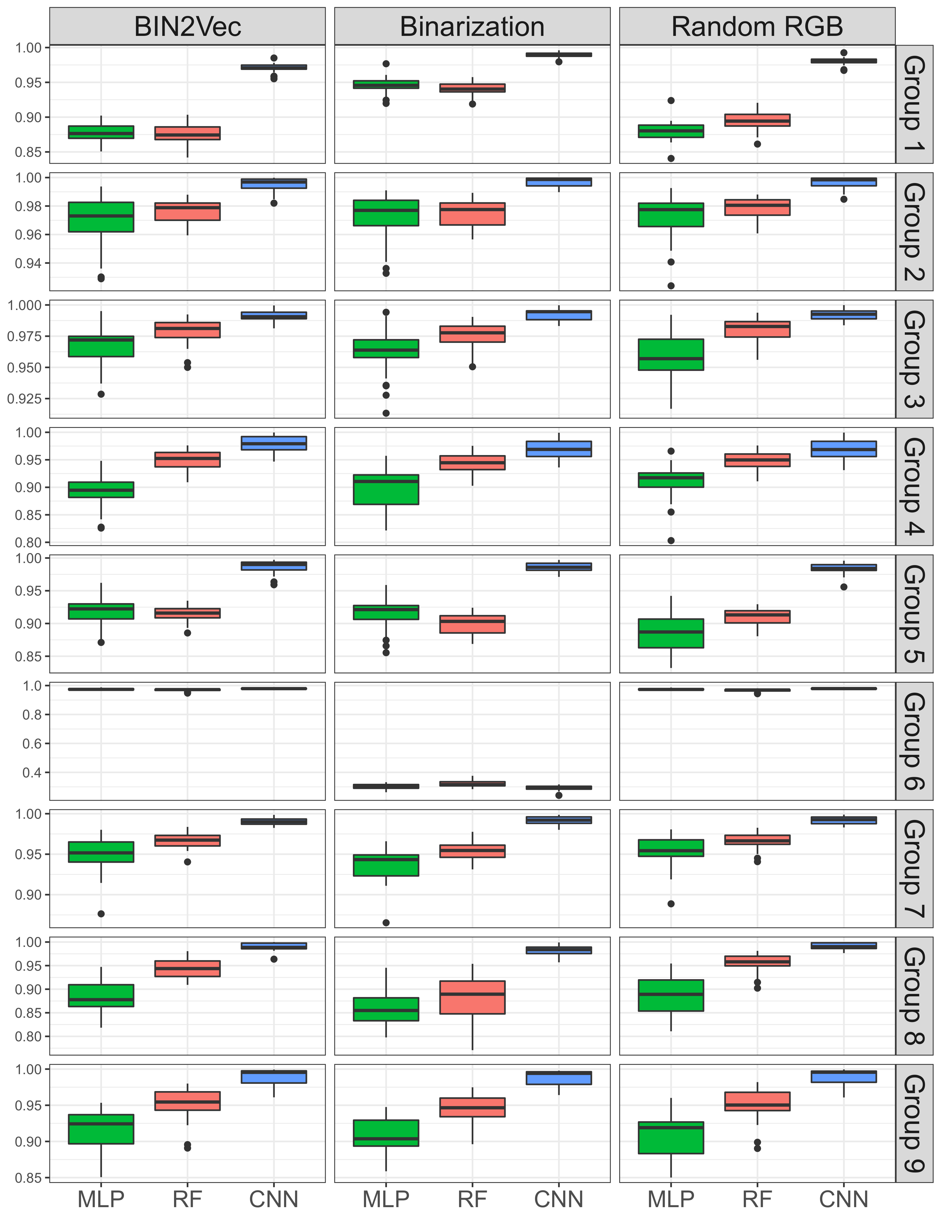
5. Results
6. Conclusions
Author Contributions
Funding
Conflicts of Interest
References
- Yoo, Y.; An, D.; Park, S.H.; Baek, J.G. Wafer map image analysis methods in semiconductor manufacturing system. J. Korean Inst. Ind. Eng. 2015, 41, 267–274. [Google Scholar]
- Ahn, J.I.; Ahn, T.H. The semiconductor quality management using the map pattern index. J. Korea Manag. Eng. Soc. 2017, 22, 61–75. [Google Scholar]
- Uzsoy, R.; Lee, C.Y.; Martin-Vega, L.A. A review of production planning and scheduling models in the semiconductor industry part I: System characteristics, performance evaluation and production planning. IIE Trans. 1992, 24, 47–60. [Google Scholar] [CrossRef]
- Cheng, J.W.; Ooi, M.P.L.; Chan, C.; Kuang, Y.C.; Demidenko, S. Evaluating the performance of different classification algorithms for fabricated semiconductor wafers. In Proceedings of the Fifth IEEE International Symposium on Electronic Design, Test and Application (DELTA’10), Ho Chi Minh City, Vietnam, 13–15 January 2010; pp. 360–366. [Google Scholar]
- Wang, C.H.; Kuo, W.; Bensmail, H. Detection and classification of defect patterns on semiconductor wafers. IIE Trans. 2006, 38, 1059–1068. [Google Scholar] [CrossRef]
- Chang, C.W.; Chao, T.M.; Horng, J.T.; Lu, C.F.; Yeh, R.H. Development pattern recognition model for the classification of circuit probe wafer maps on semiconductors. IEEE Trans. Compon. Packag. Manuf. Technol. 2012, 2, 2089–2097. [Google Scholar] [CrossRef]
- Wang, C.H. Separation of composite defect patterns on wafer bin map using support vector clustering. Expert Syst. Appl. 2009, 36, 2554–2561. [Google Scholar] [CrossRef]
- Kim, Y. Convolutional neural networks for sentence classification. arXiv, 2014; arXiv:1408.5882. [Google Scholar]
- Nallapati, R.; Zhai, F.; Zhou, B. SummaRuNNer: A recurrent neural network based sequence model for extractive summarization of documents. In Proceedings of the Thirty-First AAAI Conference on Artificial Intelligence, San Francisco, CA, USA, 4–10 February 2017; pp. 3075–3081. [Google Scholar]
- Krizhevsky, A.; Sutskever, I.; Hinton, G.E. Imagenet classification with deep convolutional neural networks. In Proceedings of the Neural Information Processing Systems, Lake Tahoe, NV, USA, 3–6 December 2012; pp. 1097–1105. [Google Scholar]
- Simonyan, K.; Zisserman, A. Very deep convolutional networks for large-scale image recognition. arXiv, 2014; arXiv:1409.1556. [Google Scholar]
- Szegedy, C.; Liu, W.; Jia, Y.; Sermanet, P.; Reed, S.; Anguelov, D.; Erhan, D.; Vanhoucke, V.; Rabinovich, A. Going deeper with convolutions. In Proceedings of the IEEE Conference on Computer Vision and Pattern Recognition, Boston, MA, USA, 7–12 June 2015; pp. 1–9. [Google Scholar]
- He, K.; Zhang, X.; Ren, S.; Sun, J. Deep residual learning for image recognition. In Proceedings of the IEEE Conference on Computer Vision and Pattern Recognition, Las Vegas, NV, USA, 27–30 June 2016; pp. 770–778. [Google Scholar]
- Huang, G.; Liu, Z.; Weinberger, K.Q.; van der Maaten, L. Densely connected convolutional networks. arXiv, 2016; arXiv:1608.06993. [Google Scholar]
- Yu, D.; Li, J. Recent progresses in deep learning based acoustic models. IEEE/CAA J. Autom. Sin. 2017, 4, 396–409. [Google Scholar] [CrossRef]
- Huang, C.J.; Wu, C.F.; Wang, C.C. Image processing techniques for wafer defect cluster identification. IEEE Des. Test Comput. 2002, 19, 44–48. [Google Scholar] [CrossRef]
- Wang, C.H. Recognition of semiconductor defect patterns using spectral clustering. In Proceedings of the IEEE International Conference on Industrial Engineering and Engineering Management, Singapore, 2–4 December 2007; pp. 587–591. [Google Scholar]
- Ooi, M.P.L.; Sim, E.K.J.; Kuang, Y.C.; Kleeman, L.; Chan, C.; Demidenko, S. Automatic defect cluster extraction for semiconductor wafers. In Proceedings of the IEEE Instrumentation and Measurement Technology Conference (I2MTC), Torino, Italy, 22–25 May 2010; pp. 1024–1029. [Google Scholar]
- Taha, K.; Salah, K.; Yoo, P.D. Clustering the dominant defective patterns in semiconductor wafer maps. IEEE Trans. Semicond. Manuf. 2017, 31, 156–165. [Google Scholar] [CrossRef]
- Liu, C.W.; Chien, C.F. An intelligent system for wafer bin map defect diagnosis: An empirical study for semiconductor manufacturing. Eng. Appl. Artif. Intel. 2013, 26, 1479–1486. [Google Scholar] [CrossRef]
- Feng, X.; Kong, X.; Ma, H. Coupled cross-correlation neural network algorithm for principal singular triplet extraction of a cross-covariance matrix. IEEE/CAA J. Autom. Sin. 2016, 3, 149–156. [Google Scholar]
- Li, T.S.; Huang, C.L. Defect spatial pattern recognition using a hybrid SOM–SVM approach in semiconductor manufacturing. Expert Syst. Appl. 2009, 36, 374–385. [Google Scholar] [CrossRef]
- Liao, C.S.; Hsieh, T.J.; Huang, Y.S.; Chien, C.F. Similarity searching for defective wafer bin maps in semiconductor manufacturing. IEEE Trans. Autom. Sci. Eng. 2014, 11, 953–960. [Google Scholar] [CrossRef]
- Adly, F.; Alhussein, O.; Yoo, P.D.; Al-Hammadi, Y.; Taha, K.; Muhaidat, S.; Jeong, Y.S.; Lee, U.; Ismail, M. Simplified subspaced regression network for identification of defect patterns in semiconductor wafer maps. IEEE Trans. Ind. Inf. 2015, 11, 1267–1276. [Google Scholar] [CrossRef]
- Adly, F.; Yoo, P.D.; Muhaidat, S.; Al-Hammadi, Y.; Lee, U.; Ismail, M. Randomized general regression network for identification of defect patterns in semiconductor wafer maps. IEEE Trans. Semicond. Manuf. 2015, 28, 145–152. [Google Scholar] [CrossRef]
- Wu, M.J.; Jang, J.S.R.; Chen, J.L. Wafer map failure pattern recognition and similarity ranking for large-scale data sets. IEEE Trans. Semicond. Manuf. 2015, 28, 1–12. [Google Scholar]
- Mikolov, T.; Sutskever, I.; Chen, K.; Corrado, G.S.; Dean, J. Distributed representations of words and phrases and their compositionality. In Proceedings of the Neural Information Processing Systems, Lake Tahoe, NV, USA, 5–10 December 2013; pp. 3111–3119. [Google Scholar]
- Mikolov, T.; Chen, K.; Corrado, G.; Dean, J. Efficient estimation of word representations in vector space. arXiv, 2013; arXiv:1301.3781. [Google Scholar]
- Goldberg, Y.; Levy, O. word2vec Explained: Deriving Mikolov et al.’s negative-sampling word-embedding method. arXiv, 2014; arXiv:1402.3722. [Google Scholar]
- Dyer, C. Notes on noise contrastive estimation and negative sampling. arXiv, 2014; arXiv:1410.8251. [Google Scholar]
- Ren, S.; He, K.; Girshick, R.; Sun, J. Faster r-cnn: Towards real-time object detection with region proposal networks. In Proceedings of the Neural Information Processing Systems, Montreal, QC, Canada, 7–12 December 2015; pp. 91–99. [Google Scholar]
- Ronneberger, O.; Fischer, P.; Brox, T. U-net: Convolutional networks for biomedical image segmentation. In Proceedings of the International Conference on Medical Image Computing and Computer-Assisted Intervention, Munich, Germany, 5–9 October 2015; Springer: Cham, Switzerland, 2015; pp. 234–241. [Google Scholar]
- Gao, S.; Zhou, M.C.; Wang, Y.; Cheng, J.; Yachi, H.; Wang, J. Dendritic neuron model with effective learning algorithms for classification, approximation, and prediction. IEEE Trans. Neural Netw. Learn. Syst. 2018, 30, 601–614. [Google Scholar] [CrossRef] [PubMed]
- Ioffe, S.; Szegedy, C. Batch normalization: Accelerating deep network training by reducing internal covariate shift. In Proceedings of the International Conference on Machine Learning, Lille, France, 6–11 July 2015; pp. 448–456. [Google Scholar]
- Deng, J.; Dong, W.; Socher, R.; Li, L.J.; Li, K.; Fei-Fei, L. Imagenet: A large-scale hierarchical image database. In Proceedings of the IEEE Conference on Computer Vision and Pattern Recognition (CVPR 2009), Miami Beach, FL, USA, 20–25 June 2009; pp. 248–255. [Google Scholar]
- Kingma, D.; Ba, J. Adam: A method for stochastic optimization. arXiv, 2014; arXiv:1412.6980. [Google Scholar]
- Srivastava, N.; Hinton, G.E.; Krizhevsky, A.; Sutskever, I.; Salakhutdinov, R. Dropout: A simple way to prevent neural networks from overfitting. J. Mach. Learn. Res. 2014, 15, 1929–1958. [Google Scholar]
- Breiman, L. Random forests. Mach. Learn. 2001, 45, 5–32. [Google Scholar] [CrossRef]
- Fernández-Delgado, M.; Cernadas, E.; Barro, S.; Amorim, D. Do we need hundreds of classifiers to solve real world classification problems. J. Mach. Learn. Res. 2014, 15, 3133–3181. [Google Scholar]
- Maaten, L.V.D.; Hinton, G. Visualizing data using t-SNE. J. Mach. Learn. Res. 2008, 9, 2579–2605. [Google Scholar]

| Value | Description |
|---|---|
| −2 | Non-wafer part |
| −1 | Untested portion |
| 0 | Not all results from 1 to 9999 |
| 1∼9999 | Code indicating a set of EDS tests that the die does not pass |
| Group | No. Wafers | No. Good | No. Bad | Good (%) | Bad (%) | No. Bins | No. Dies (Horizontal) | No. Chips (Vertical) |
|---|---|---|---|---|---|---|---|---|
| 1 | 5464 | 4156 | 1308 | 76.06 | 23.94 | 401 | 23 | 27 |
| 2 | 5449 | 4771 | 678 | 87.56 | 12.44 | 77 | 29 | 50 |
| 3 | 3261 | 2621 | 640 | 80.37 | 19.63 | 43 | 41 | 36 |
| 4 | 2781 | 2578 | 203 | 92.70 | 7.30 | 108 | 47 | 62 |
| 5 | 2543 | 2145 | 398 | 84.35 | 15.65 | 371 | 29 | 26 |
| 6 | 2101 | 850 | 1251 | 40.46 | 59.54 | 8 | 32 | 38 |
| 7 | 1958 | 1403 | 555 | 71.65 | 28.35 | 82 | 33 | 58 |
| 8 | 1799 | 1535 | 264 | 85.33 | 14.67 | 206 | 26 | 26 |
| 9 | 1715 | 1542 | 173 | 89.91 | 10.09 | 108 | 47 | 51 |
| Actual Class | |||
|---|---|---|---|
| Bad (Positive) | Good (Negative) | ||
| Predicted Class | Bad (Positive) | True Positive (TP) | False Positive (FP) |
| Good (Negative) | False Negative (FN) | True Negative (TN) | |
| Binary | Random RGB | Bin2Vec | |||||||||||||||||
|---|---|---|---|---|---|---|---|---|---|---|---|---|---|---|---|---|---|---|---|
| Group | Model | REC | PRE | ACC | F1 | BCR | AUC | REC | PRE | ACC | F1 | BCR | AUC | REC | PRE | ACC | F1 | BCR | AUC |
| 1 | MLP | 83.72 (3.28) | 82.45 (2.62) | 91.81 (1.08) | 83.03 (2.28) | 88.86 (1.797) | 0.946 (0.011) | 61.46 (3.43) | 74.11 (3.06) | 85.61 (1.07) | 67.14 (2.64) | 75.66 (2.10) | 0.880 (0.014) | 61.77 (3.17) | 73.61 (3.10) | 85.52 (1.11) | 67.12 (2.62) | 75.77 (2.01) | 0.877 (0.013) |
| RF | 83.06 (2.84) | 79.51 (2.38) | 90.72 (1.00) | 81.21 (1.92) | 87.96 (1.57) | 0.941 (0.010) | 71.04 (3.14) | 65.56 (2.55) | 83.97 (1.33) | 68.15 (2.32) | 79.10 (1.91) | 0.894 (0.013) | 65.64 (2.93) | 69.25 (2.51) | 84.65 (1.15) | 67.36 (2.30) | 77.15 (1.84) | 0.876 (0.015) | |
| CNN | 91.40 (1.97) | 92.85 (1.90) | 96.25 (0.65) | 92.10 (1.37) | 94.53 (1.04) | 0.989 (0.004) | 88.56 (2.04) | 91.04 (1.85) | 95.17 (0.66) | 89.76 (1.40) | 92.80 (1.09) | 0.981 (0.005) | 87.06 (2.10) | 91.04 (1.95) | 94.84 (0.55) | 88.98 (1.19) | 92.02 (1.02) | 0.971 (0.006) | |
| 2 | MLP | 89.07 (3.82) | 88.93 (2.41) | 97.25 (0.55) | 88.95 (2.33) | 93.60 (2.01) | 0.972 (0.016) | 89.53 (4.04) | 90.06 (3.12) | 97.45 (0.67) | 89.74 (2.75) | 93.92 (2.14) | 0.972 (0.016) | 86.40 (3.43) | 89.77 (2.40) | 97.07 (0.57) | 88.02 (2.43) | 92.28 (1.88) | 0.970 (0.019) |
| RF | 87.21 (3.39) | 84.17 (2.51) | 96.37 (0.61) | 85.63 (2.34) | 92.28 (1.83) | 0.975 (0.009) | 87.10 (3.24) | 84.57 (2.24) | 96.43 (0.53) | 85.78 (2.07) | 92.25 (1.72) | 0.978 (0.008) | 86.97 (3.51) | 83.36 (1.90) | 96.23 (0.46) | 85.08 (1.94) | 92.09 (1.83) | 0.976 (0.008) | |
| CNN | 96.08 (1.31) | 96.07 (1.59) | 99.02 (0.21) | 96.06 (0.84) | 97.74 (0.63) | 0.997 (0.003) | 95.76 (1.91) | 96.32 (1.67) | 99.01 (0.25) | 96.02 (1.02) | 97.59 (0.93) | 0.996 (0.004) | 95.69 (1.54) | 94.45 (1.63) | 99.02 (0.26) | 96.05 (1.04) | 97.57 (0.77) | 0.995 (0.005) | |
| 3 | MLP | 86.56 (3.50) | 92.47 (2.68) | 95.98 (0.97) | 89.39 (2.63) | 92.22 (1.98) | 0.962 (0.018) | 85.05 (4.85) | 94.59 (2.19) | 96.12 (1.09) | 89.51 (3.16) | 91.64 (2.68) | 0.958 (0.018) | 86.02 (4.63) | 94.46 (2.43) | 96.26 (1.06) | 89.98 (3.01) | 82.14 (2.54) | 0.968 (0.017) |
| RF | 87.41 (3.98) | 93.44 (2.18) | 96.38 (0.95) | 90.27 (2.54) | 92.78 (2.17) | 0.976 (0.010) | 87.98 (3.62) | 94.31 (2.07) | 96.66 (0.85) | 90.99 (2.35) | 93.18 (1.97) | 0.980 (0.009) | 97.95 (4.14) | 94.54 (2.00) | 96.70 (0.91) | 91.07 (2.54) | 93.19 (2.22) | 0.979 (0.010) | |
| CNN | 96.15 (1.33) | 97.69 (1.28) | 98.80 (0.30) | 96.90 (0.77) | 97.78 (0.64) | 0.992 (0.005) | 95.91 (1.31) | 98.36 (1.08) | 98.88 (0.32) | 97.11 (0.83) | 97.74 (0.67) | 0.992 (0.005) | 95.99 (1.56) | 98.12 (0.89) | 98.85 (0.35) | 97.03 (0.92) | 97.75 (0.80) | 0.991 (0.005) | |
| 4 | MLP | 62.11 (6.98) | 70.40 (5.95) | 95.27 (0.69) | 65.81 (5.59) | 77.86 (4.48) | 0.897 (0.036) | 63.74 (6.95) | 74.26 (5.95) | 95.67 (0.63) | 68.30 (5.04) | 78.99 (4.36) | 0.911 (0.032 ) | 60.24 (7.17) | 73.00 (6.73) | 95.39 (0.70) | 65.70 (5.49) | 76.77 (4.56) | 0.892 (0.030) |
| RF | 85.07 (5.21) | 55.00 (4.89) | 93.83 (0.90) | 66.67 (4.27) | 89.61 (2.67) | 0.944 (0.019) | 83.59 (5.36) | 58.37 (6.66) | 94.42 (1.07) | 68.55 (5.53) | 89.19 (2.89) | 0.948 (0.018) | 84.23 (5.21) | 58.52 (6.21) | 94.48 (1.03) | 68.93 (5.47) | 89.53 (2.83) | 0.949 (0.018) | |
| CNN | 83.25 (5.39) | 90.96 (3.82) | 98.15 (0.43) | 86.80 (3.25) | 90.89 (2.91) | 0.970 (0.018) | 86.59 (4.52) | 91.00 (4.57) | 98.37 (0.50) | 88.64 (3.43) | 92.70 (2.44) | 0.970 (0.018) | 87.15 (4.88) | 91.79 (4.50) | 98.46 (0.47) | 89.28 (3.23) | 93.02 (2.58) | 0.979 (0.014) | |
| 5 | MLP | 83.46 (5.94) | 58.65 (4.25) | 88.05 (1.74) | 68.74 (3.82) | 86.07 (3.02) | 0.914 (0.025) | 78.00 (5.83) | 57.52 (3.66) | 87.43 (1.49) | 66.09 (3.65) | 83.34 (3.09) | 0.886 (0.030) | 77.42 (5.27) | 61.85 (3.76) | 88.90 (1.34) | 68.67 (3.62) | 83.90 (2.88) | 0.917 (0.021) |
| RF | 80.64 (4.62) | 54.08 (4.01) | 86.25 (1.33) | 64.61 (3.30) | 83.85 (2.26) | 0.898 (0.016) | 74.99 (5.31) | 57.90 (4.13) | 87.56 (1.28) | 65.22 (3.61) | 82.05 (2.93) | 0.909 (0.013) | 83.82 (4.09) | 54.56 (4.20) | 86.54 (1.48) | 65.99 (3.55) | 85.39 (2.22) | 0.914 (0.012) | |
| CNN | 85.17 (4.77) | 89.87 (4.45) | 96.10 (0.77) | 87.27 (2.40) | 91.38 (2.26) | 0.986 (0.007) | 90.04 (2.85) | 89.52 (3.74) | 96.75 (0.68) | 89.71 (2.04) | 93.92 (1.40) | 0.984 (0.009) | 89.50 (3.62) | 89.93 (3.37) | 96.75 (0.64) | 89.63 (2.04) | 93.68 (1.79) | 0.986 (0.010) | |
| 6 | MLP | 47.30 (32.57) | 84.23 (12.88) | 58.48 (5.90) | 51.99 (17.30) | 49.77 (2.71) | 0.301 (0.017) | 92.59 (2.09) | 91.70 (1.40) | 90.58 (1.67) | 92.13 (1.43) | 90.05 (1.66) | 0.974 (0.006) | 92.27 (2.85) | 91.81 (1.58) | 90.45 (1.47) | 92.00 (1.34) | 89.96 (1.38) | 0.975 (0.006) |
| RF | 28.40 (12.73) | 89.56 (6.00) | 54.94 (2.51) | 41.64 (7.20) | 49.88 (2.43) | 0.321 (0.020) | 93.18 (2.17) | 90.81 (1.88) | 90.35 (1.49) | 91.95 (1.28) | 89.65 (1.55) | 0.967 (0.009) | 93.01 (2.33) | 90.78 (1.94) | 90.25 (1.62) | 91.86 (1.41) | 89.56 (1.66) | 0.970 (0.008) | |
| CNN | 97.19 (0.94) | 65.76 (1.07) | 68.14 (1.52) | 78.44 (0.90) | 49.44 (3.30) | 0.292 (0.016) | 94.48 (1.12) | 91.81 (1.49) | 91.66 (1.15) | 93.11 (0.93) | 90.92 (1.34) | 0.979 (0.005) | 94.38 (1.17) | 91.84 (1.47) | 91.64 (1.18) | 93.09 (0.96) | 90.91 (1.35) | 0.979 (0.005) | |
| 7 | MLP | 82.43 (4.20) | 85.65 (3.64) | 91.07 (1.54) | 83.93 (2.87) | 88.22 (2.28) | 0.937 (0.020) | 84.99 (4.61) | 90.50 (3.25) | 93.20 (1.64) | 87.58 (3.15) | 90.50 (2.57) | 0.954 (0.019) | 84.60 (5.13) | 89.75 (3.39) | 92.88 (1.84) | 87.02 (3.55) | 90.15 (2.90) | 0.950 (0.022) |
| RF | 80.99 (3.18) | 90.62 (3.53) | 92.13 (1.18) | 85.46 (2.24) | 88.44 (1.70) | 0.953 (0.012) | 84.10 (3.75) | 93.28 (2.63) | 93.69 (1.26) | 88.39 (2.29) | 90.55 (1.98) | 0.966 (0.011) | 84.06 (3.64) | 92.48 (2.71) | 93.44 (1.23) | 88.00 (2.08) | 90.38 (1.86) | 0.967 (0.010) | |
| CNN | 94.60 (1.97) | 96.67 (1.95) | 97.53 (0.75) | 95.60 (1.34) | 96.62 (1.04) | 0.992 (0.005) | 95.47 (1.63) | 97.04 (1.62) | 97.88 (0.59) | 96.23 (1.04) | 97.13 (0.83) | 0.992 (0.004) | 95.35 (1.76) | 96.71 (1.68) | 97.76 (0.63) | 96.01 (1.12) | 97.01 (0.89) | 0.990 (0.004) | |
| 8 | MLP | 67.55 (6.43) | 61.51 (5.80) | 88.91 (1.71) | 64.21 (5.02) | 79.00 (3.79) | 0.858 (0.038) | 68.81 (5.73) | 79.56 (4.89) | 92.78 (1.14) | 73.66 (4.35) | 81.59 (3.39) | 0.886 (0.040) | 66.16 (5.08) | 84.97 (5.29) | 93.26 (0.98) | 74.25 (3.90) | 80.44 (3.03) | 0.884 (0.033) |
| RF | 63.74 (5.68) | 84.14 (4.21) | 93.11 (1.18) | 72.36 (3.93) | 78.96 (3.46) | 0.878 (0.048) | 71.90 (6.75) | 85.09 (5.45) | 94.17 (1.16) | 77.66 (4.20) | 83.81 (3.83) | 0.956 (0.020) | 70.84 (5.82) | 87.28 (4.88) | 94.34 (1.13) | 77.00 (3.81) | 83.37 (3.36) | 0.944 (0.020) | |
| CNN | 87.23 (4.37) | 93.30 (3.91) | 97.18 (0.87) | 90.08 (3.04) | 92.85 (2.34) | 0.982 (0.010) | 91.89 (4.00) | 97.21 (2.59) | 98.41 (0.70) | 94.41 (2.48) | 95.61 (2.09) | 0.991 (0.007) | 92.14 (3.58) | 96.73 (2.83) | 98.37 (0.65) | 94.32 (2.27) | 95.70 (1.85) | 0.991 (0.008) | |
| 9 | MLP | 63.71 (7.28) | 71.14 (6.67) | 93.61 (0.88) | 66.86 (4.89) | 78.47 (4.43) | 0.909 (0.022) | 51.14 (5.83) | 72.92 (7.60) | 93.05 (0.88) | 59.89 (5.37) | 70.61 (4.07) | 0.907 (0.031) | 65.33 (7.72) | 73.61 (5.90) | 94.03 (0.80) | 68.87 (4.70) | 79.58 (4.54) | 0.914 (0.030) |
| RF | 74.94 (7.34) | 68.04 (7.68) | 93.98 (1.17) | 71.05 (5.95) | 84.76 (4.15) | 0.946 (0.020) | 85.68 (6.28) | 64.68 (6.44) | 93.92 (1.18) | 73.54 (5.48) | 90.08 (3.39) | 0.951 (0.022) | 85.45 (6.47) | 63.28 (6.06) | 93.63 (1.05) | 72.50 (4.92) | 89.81 (3.34) | 0.951 (0.022) | |
| CNN | 85.24 (5.31) | 89.05 (4.98) | 97.40 (0.70) | 86.95 (3.61) | 91.72 (2.86) | 0.989 (0.010) | 87.81 (5.56) | 90.62 (4.01) | 97.81 (0.62) | 89.04 (3.24) | 93.16 (2.92) | 0.990 (0.010) | 86.67 (4.82) | 90.58 (4.83) | 97.69 (0.61) | 88.43 (3.02) | 92.57 (2.49) | 0.989 (0.012) | |
© 2019 by the authors. Licensee MDPI, Basel, Switzerland. This article is an open access article distributed under the terms and conditions of the Creative Commons Attribution (CC BY) license (http://creativecommons.org/licenses/by/4.0/).
Share and Cite
Kim, J.; Kim, H.; Park, J.; Mo, K.; Kang, P. Bin2Vec: A Better Wafer Bin Map Coloring Scheme for Comprehensible Visualization and Effective Bad Wafer Classification. Appl. Sci. 2019, 9, 597. https://doi.org/10.3390/app9030597
Kim J, Kim H, Park J, Mo K, Kang P. Bin2Vec: A Better Wafer Bin Map Coloring Scheme for Comprehensible Visualization and Effective Bad Wafer Classification. Applied Sciences. 2019; 9(3):597. https://doi.org/10.3390/app9030597
Chicago/Turabian StyleKim, Junhong, Hyungseok Kim, Jaesun Park, Kyounghyun Mo, and Pilsung Kang. 2019. "Bin2Vec: A Better Wafer Bin Map Coloring Scheme for Comprehensible Visualization and Effective Bad Wafer Classification" Applied Sciences 9, no. 3: 597. https://doi.org/10.3390/app9030597
APA StyleKim, J., Kim, H., Park, J., Mo, K., & Kang, P. (2019). Bin2Vec: A Better Wafer Bin Map Coloring Scheme for Comprehensible Visualization and Effective Bad Wafer Classification. Applied Sciences, 9(3), 597. https://doi.org/10.3390/app9030597