Article

Femtosecond Laser Irradiation of Carbon Nanotubes to Metal Electrodes

1
State Key Laboratory for Manufacturing System Engineering, Xi’an Jiaotong University, Xi’an 710049, China
2
State Key Laboratory of Fluid Power and Mechatronic Systems, Zhejiang University, Hangzhou 310027, China
3
Shaanxi Key Laboratory of Intelligent Robots, Xi’an Jiaotong University, Xi’an 710049, China
4
State Key Laboratory of Transient Optics and Photonics, Xi’an Institute of Optics and Precision Mechanics of Chinese Academy of Sciences, Xi’an 710119, China
5
School of Construction Machinery, Chang’an University, Xi’an 710064, China
*
Author to whom correspondence should be addressed.
Appl. Sci. 2019, 9(3), 476; https://doi.org/10.3390/app9030476
Submission received: 12 December 2018 / Revised: 22 January 2019 / Accepted: 28 January 2019 / Published: 30 January 2019
(This article belongs to the Special Issue Selected Papers from the NMJ2018)

Abstract

:
Carbon nanotubes (CNTs) have excellent performance, which means that they could be better electrical conductors. However, the problem of the connection of CNTs to electrodes limits their application. Particularly, improving connection efficiency while ensuring the quality of the connection is a big challenge, because it is difficult to form Ohmic contact between CNTs and electrodes. To address this issue, we propose the use of a femtosecond laser to irradiate the contact surface between the CNTs and the electrodes to obtain a good connection quality and electrical performance. At the same time, since the laser-induced connection acts on all the contact surfaces in the irradiation area, the connection efficiency can be improved, which provides a new idea for the large-scale preparation of the connection.

1. Introduction

As a new type of one-dimensional nanomaterial, carbon nanotubes (CNTs) have been proved to have excellent performance in electrical, mechanical and thermal fields, and have broad application prospects in the manufacture of Micro-Nano devices [1,2]. However, the excellent electrical properties of CNTs cannot be reflected very well due to the difficulty in forming a reliable Ohmic contact between the CNTs and the electrodes in the preparation of the Micro-Nano devices. Therefore, the development of Micro-Nano devices based on CNTs is restricted [3]. The main problem is that when the size of the connection and the accuracy of the interconnection become more than a certain scale range, the energy field law and connection principle of the connect process make a qualitative change due to the size effect, which will seriously restrict the reliability and stability of CNTs-based electronic device connects. In order to solve this problem, various physical or chemical methods have been explored to achieve a connection [4,5,6,7,8,9]. For example, Li [10] obtained good results using rapid annealing to reduce the electrical resistance of the contact surface between the CNTs and electrodes. However, the method may damage the CNTs in a large area or cause damage to a circuit composed of low-melting-point material. Kim [11] used electron beam-induced deposition (EBID) technology to deposit graphitized carbon, which achieved Ohmic contact between end-opening multi-walled carbon nanotubes (MWCNTs) and metal electrodes in the low temperature manufacturing process. However, because the deposition solder at a specific location is difficult to achieve and may affect certain circuits, it is hard to meet the needs of large-scale fabrication with this method.
Laser beams have been used in the fabrication of Micro-Nano devices widely. They mainly depend upon the thermal effect of laser to realize the connection between CNTs and the metal electrodes. The connection effect obtained by laser irradiation has the advantages of smaller contact resistance [12], higher stability and better mechanical properties, compared with other physical or chemical methods [13,14,15,16]. However, the reduction of the size of the electrodes and the thickness results in significant size effect [17]; therefore, the higher laser power radiates the thermal effect of the metal surface to destroy the metal surface, which is unacceptable. A lower laser power does not form enough heat accumulation on the surface to make a connection possible.
In this paper, we used femtosecond laser illumination to connect single-walled carbon nanotubes (SWCNTs) and MWCNTs to the electrodes. The femtosecond laser pulse width is smaller than the electron cooling time, making it possible to add significant energy to the target material before mechanical or thermal responses can take place [18], and the damage of the surface morphology of the electrode by heat accumulation can be avoided. At the same time, femtosecond laser irradiation will cause Plasmon resonance on the metal surface, accelerating the atom diffusion inside the material, thereby realizing the connection between the CNTs and the electrodes [19]. The characterization and analysis of the experimental results show that under the irradiation of a femtosecond laser, both SWCNTs and MWCNTs have a good connection with the electrodes. The resistance of the SWCNTs in contact with the electrodes was tested, and the results showed that it was greatly reduced.

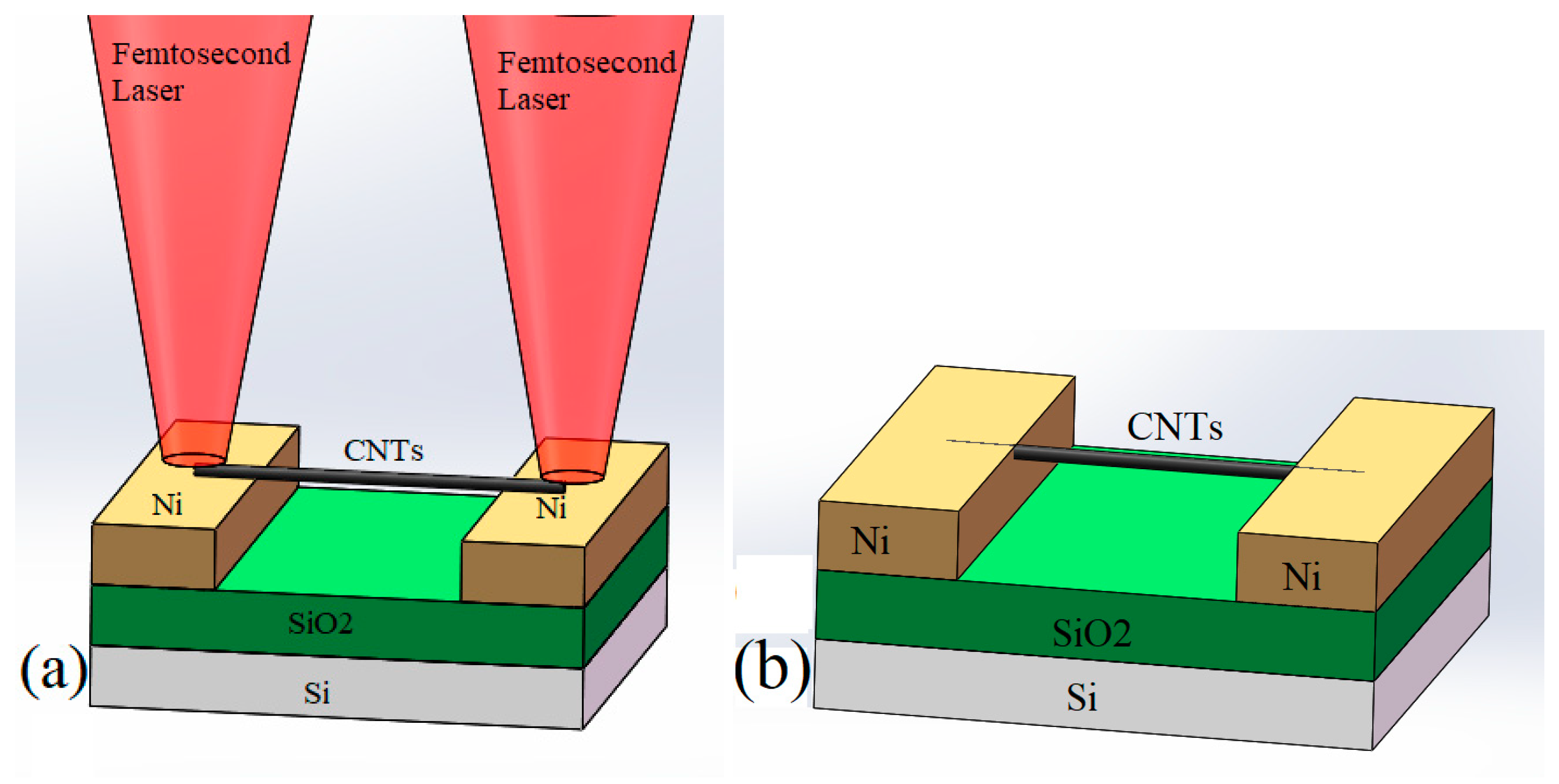
2. Experimental Details

Single-walled carbon nanotubes (SWCNTs) with a diameter of 1–2 nm from XFNANO Co. Ltd (Nanjing, China). were used in this experiment, as were multi-walled carbon nanotubes (MWCNTs) with a diameter of 30 nm to 50 nm. The purified CNTs were dispersed in a 1.5% mass fraction of sodium dodecyl sulfate (SDS) solution, and they were ultrasonically vibrated by an Ultrasonic cell grinder for 7 hours in a 20-degree water bath cooling to obtain a dispersed CNTs solution [20,21].
In order to obtain two metal electrodes, we grew a 500 nm thick silicon dioxide film on a 500 μm thick silicon wafer (Tebo Technology Co. Ltd., Harbin, China) by Plasma enhanced chemical vapor deposition (PECVD, ORION Ⅲ, Trion Co. Ltd., Clearwater, FL, USA). Then, the pattern of the electrode was etched on the polymethyl methacrylate (PMMA) using electron beam direct-write lithography (EBL, CABL-9000CSX, CRESTEC Co. Ltd., Tokyo, Japan) on the silicon oxide film. The electrode pattern is realized by two pieces of 120 * 120 pads connected by 180 μm -long and 80 μm wide lines. Thereafter, 100 nm thick metal Ni was sputtered by magnetron sputtering (Denton Co. Ltd., Moorestown, NJ, USA), and then the metal adhered to the PMMA was peeled off to obtain a desired electrode [22,23]. The two metal electrodes were separated by a gap of 1 μm. The structure diagram is shown in Figure 1.
A sample injector (TopPette, Dragonmed Co. Ltd., Beijing, China) was used to draw 50 μL of the dispersed SWCNTs solution onto the surface of the metal electrodes by drop coating, and allowed to naturally deposit at room temperature for 6 hours. The CNTs were naturally deposited on two metal electrodes, then immersed in deionized water for 5 minutes. After the dispersion was completely dissolved in water, it was taken out to obtain the desired sample. In order to avoid the influence of metallic CNTs or partially unstable CNT bundles on the test results, the electrical breakdown method can be used to remove them [24]. However, in the preliminary work of this experiment, we found that metallic CNTs or tube bundles were also damaged under the appropriate laser energy irradiation (less than the energy required for the connection), while the semiconducting CNTs were unaffected. Based on this phenomenon, we used this method to remove unwanted type of CNTs.
A Nd:YLE solid state femtosecond laser device (Spitfire Ace-120F, Spectra-physics Inc., Vienna, Austria) was adopted in this experiment. The laser system delivers 120-fs-width pluses and operates at wavelengths of 800 nm. The repetition frequency utilized in the experiment was 1k Hz. The laser is perpendicular to the electrode and focuses on the electrode surface and the SWCNTs port area for a fixed point scan. Different from the precise spot welding by using the atomic force microscope (AFM) probe [25,26,27,28,29,30], since the spot shape is a line, the entire edge of the electrode can be irradiated, which makes the method more efficient [31,32]. Through multiple experiments, it was found that a suitable laser energy density for connecting SWCNTs to the Ni electrodes was about 13.810 mJ/cm2, and that the irradiation duration was about 30 s. The positioning of the area to be processed and the area irradiated by the laser was achieved by means of a high-precision processing platform. The movement of the processing platform can be achieved through software programming (μFAB, NewPort Co. Ltd., Irvine, CA, USA). In this way, the laser can precisely irradiate the contact area of the electrode and the end of the CNT, thereby avoiding the influence on the area that does not need to be processed. All processing is carried out at room temperature and standard atmospheric pressure. At the same time, the surface topography of the samples before and after irradiation was observed using a field emission scanning electron microscope (FESEM, SU8010, Hitachi Co. Ltd., Tokyo, Japan). After that, we used a semiconductor device analyzer (B1500A Keysight Co. Ltd., Bayan Lepas, Malaysia) to evaluate the electrical properties before and after irradiation, respectively. The test voltage range was −5 V to 5 V, the step size was 0.05 V, and the number of steps was 201. The probes tested were lapped onto two electrodes and applied with a certain amount of voltage. Since the contact resistance between the probe and the electrode is extremely small (<10 ohms), i.e., much smaller than the contact resistance between the carbon nanotube and the metal, the influence of the contact resistance between the probe and the electrode can be neglected.

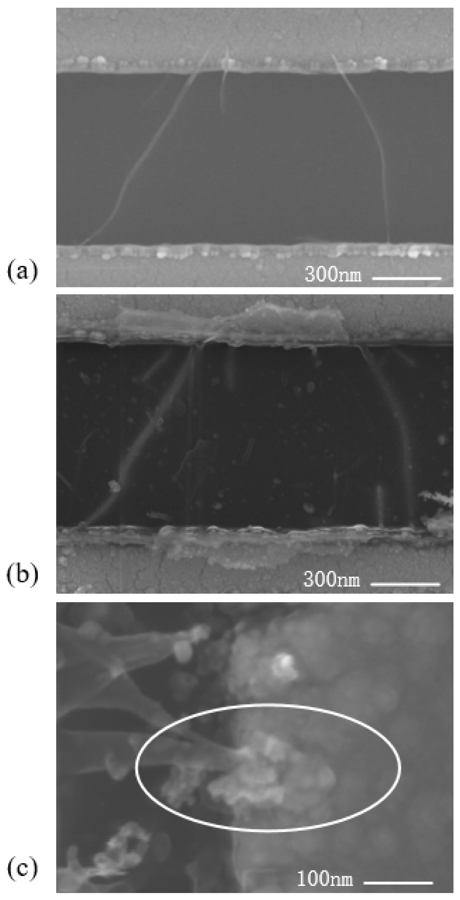
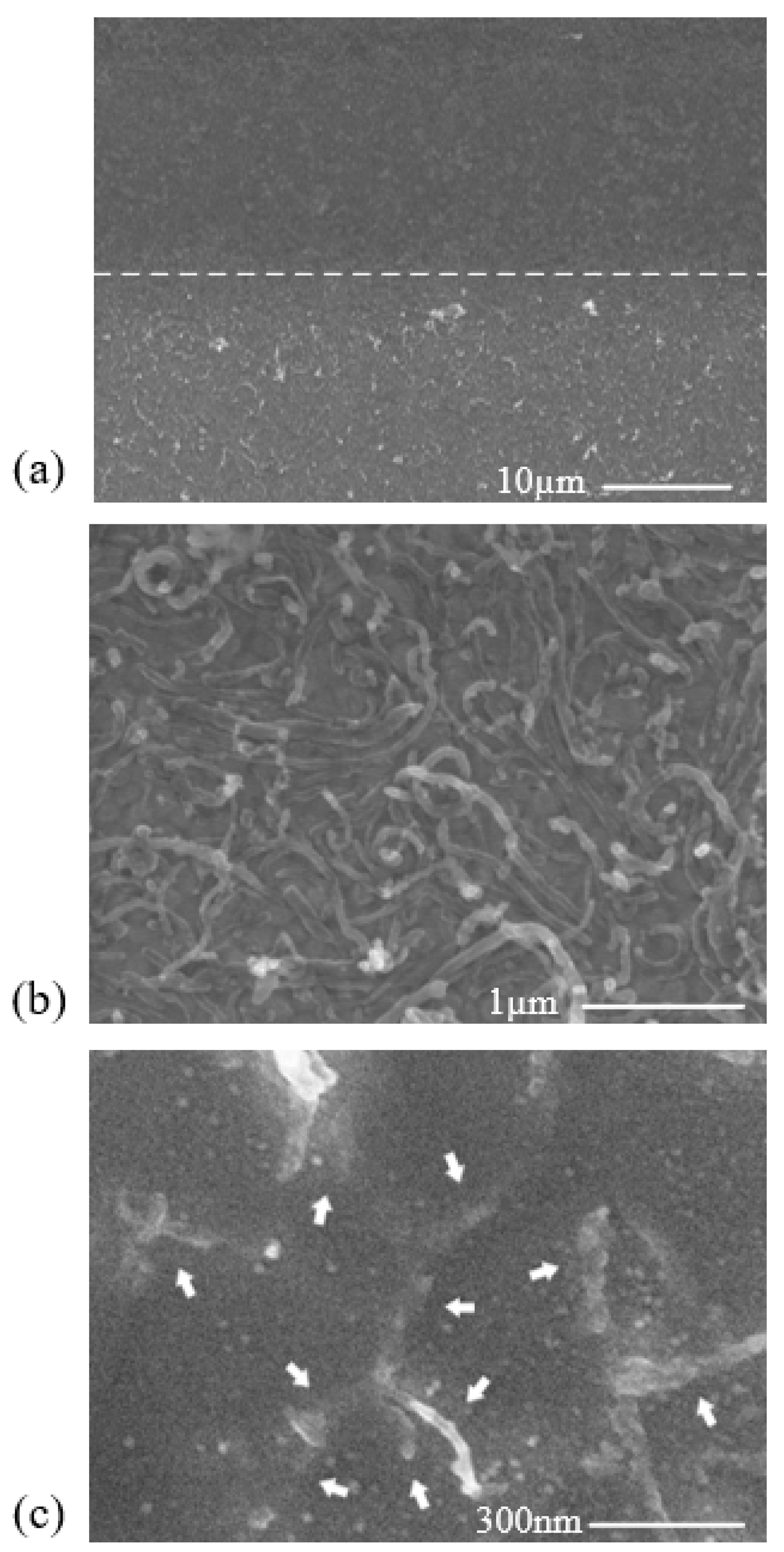
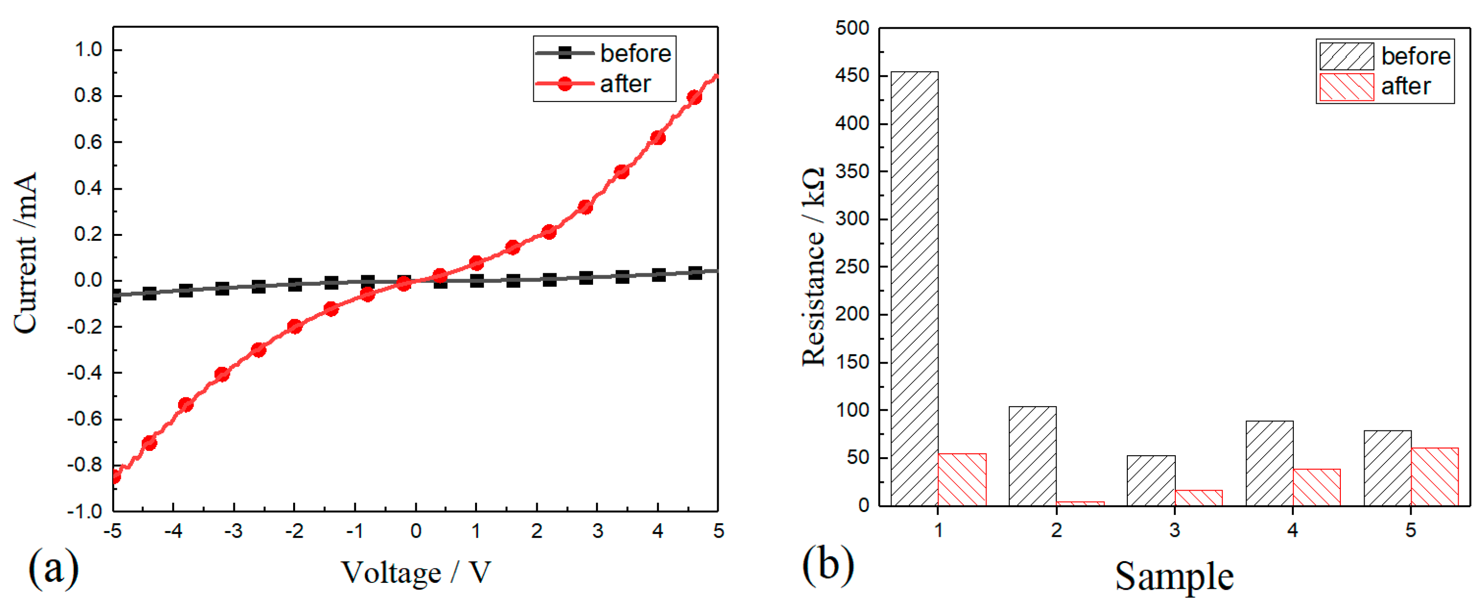
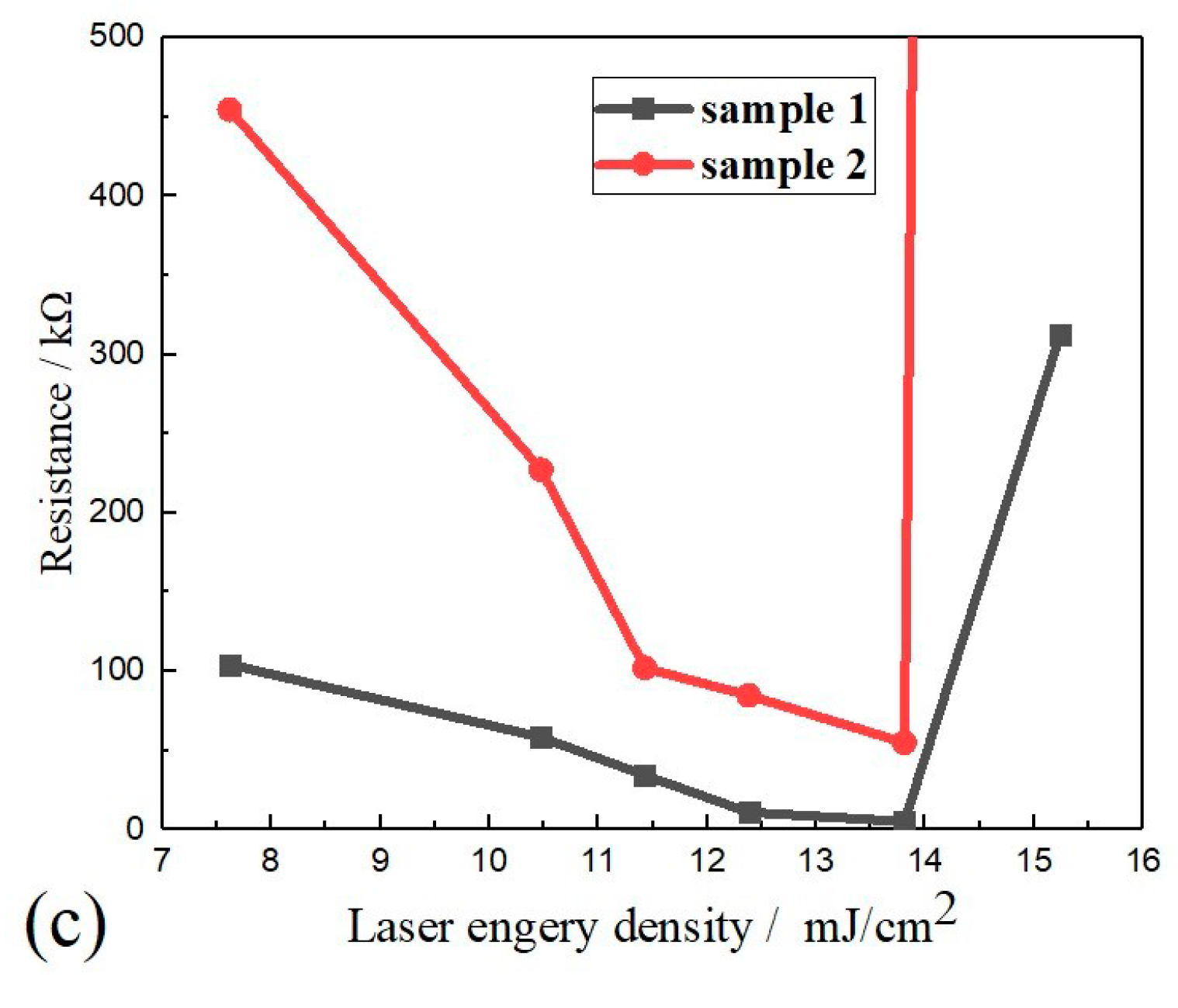
3. Results and Discussion

Before processing the electrode structure, we first tried to solder the entire CNT to the metal surface. MWCNTs were deposited on a gold surface with a thickness of 60 nm, then irradiated by laser. The laser energy density was approximately 23.810 mJ/cm2. The results of several experiments showed that the MWCNTs were embedded and welded into the metal surface after laser irradiation, and only part of the end of the CNTs were exposed. Figure 2a shows a typical scanning electron microscope (SEM) image of comparison of the laser irradiated and un-irradiated areas, with the lower half being the un-irradiated area and the upper half being the laser irradiated area with significant differences between the two areas. Figure 2b is a high-resolution SEM image before laser irradiation. It shows that the MWCNTs loosely stay on the surface of metal electrode, and the CNTs can be clearly observed. Figure 2c is a high resolution SEM image after laser irradiation, in which the arrows indicate MWCNTs embedded in the gold surface and the highlights are part of the exposed CNTs.
After that, we tried to connect the SWCNTs with the metal electrodes. Figure 3a shows a SEM image of CNTs deposited on the surface of the electrodes before laser irradiation. The morphology of the CNTs and the electrode surface can be clearly seen in the figure. At this time, the CNTs are only lying on the surface, and thus, there is a large contact resistance with the surface of the electrodes. Figure 3b shows a topographical view after laser irradiation. A certain degree of morphological change occurred on the surface of the electrodes which can be clearly observed, and the ends of CNTs were buried in the metal electrodes so that the ends of the CNTs were almost invisible in the SEM image. A partial topographical view of the CNTs-to-electrode connection is shown in Figure 3c, in which it can be clearly observed that the SWNCTs is embedded in the metal electrode.
The mechanism of the laser-induced connection is explained as follows. Femtosecond (fs) laser illumination combines high pulse intensity with ultrashort pulse duration, the metal and surrounding surface Plasmon resonance (SPR) in the irradiated region can be excited by appropriate power irradiation [33,34]. Due to the Ohmic thermal effect of the metal, SPR will only generate local electric field enhancement in a small area (sub-wavelength) [35]. When the oscillation frequency of the electron coincides with the frequency of the incident light wave, resonance will occur [36,37]. In the resonance state, the energy of the electromagnetic field transforms effectively into the collective vibrational energy of free electrons on the metal surface, thereby accelerating the electron diffusion of the contact surface between the CNTs and the metal electrodes [38]. At the same time, the surface of the electrode and the ends of CNT form a stronger local thermal field than other regions under the femtosecond laser irradiation, so that the surface at the edge of the metal electrode is slightly melted to form a molten pool [13]. The CNTs are pressed into the molten pool under the action of laser light pressure [39]. When the laser irradiation is stopped, the CNTs rapidly anneal at the junction of the electrodes, thereby firmly embedding the CNTs in the metal electrodes.
In order to evaluate the electrical properties of the contact before and after the connection, we conducted electrical performance tests on the two ends of the contact between the CNTs and the electrodes before and after the laser irradiation. We determined that there were a small number of SWCNT bundles composed of multiple SWCNTs or individual SWCNTs and SWCNT bundles connected together in the SDS solution in the experiment. After depositing on the electrodes, the SWCNT bundles might bridge to the electrodes, which may have a certain degree of influence on the test results. In this experiment, we used the method of SEM to observe the presence of SWCNT bundles, irradiating the SWCNT bundles with a low energy density (about 7.619 mJ/cm2, irradiation duration of 60 s), so that the SWCNT bundles were destroyed, while the individual SWCNTs deposited between the two electrodes was retained. It was found by SEM that a part of the SWCNTs bundle was broken, and individual SWCNTs or stable SWCNT bundles basically remained, which ensured that the test results were not affected by the quality of SWCNT bundles. Therefore, the “before irradiation” mentioned in this article, unless otherwise specified, indicates that the state after the influence of the SWCNT bundles has been removed. The removal of unstable SWCNTs by laser irradiation is still under investigation. The resistance at both ends of the measured electrodes is typically several hundred thousand ohms at room temperature before laser irradiation. After laser irradiation, the resistance is reduced to tens of thousands of ohms to several thousand ohms.
For the purpose of investigating the effect of laser energy density on the connection effect, we used different laser power parameters to irradiate the contact area and characterized the effect of connection through the I-V curve. When the laser energy density is about 11.429 mJ/cm2, the resistance at the contact is reduced from 104 k to 34.2 k ohms. When the laser energy density increases to 13.810 mJ/cm2, the resistance at the contact decreases 5.5 k ohms and then tends to saturate at 5.5 k ohms. Increasing laser density continually, a certain degree of damage begins to occur at the edge of the metal electrode; part of the CNTs are struck and thrown out, and the resistance at both ends of the electrode rises sharply. Figure 4a shows an I-V plot of one of the samples before and after laser irradiation, where the black line represents before laser irradiation and the red line represents after laser irradiation. It can be very clearly observed that the contact resistance after laser irradiation has decreased significantly compared to before laser irradiation. Figure 4b shows the change in resistance of multiple samples before and after laser irradiation. The resistance of all CNTs to metal electrodes contact resistance is based on the calculation of the I-V curve when the measured voltage is 5 V. It can be seen from the figure that although the contact resistances of the samples are different, the contact resistance has decreased to some extent after laser irradiation, indicating that the SWCNTs form a reliable connection with the metal electrodes under laser irradiation. At the same time, measurements were carried out after storage for 1 month under laboratory conditions at room temperature and atmospheric pressure, and the results were almost unchanged, indicating that the contact points were stable in the air for a long period of time. Figure 4c shows the tendency of the resistance change across the CNTs under different laser energy irradiation.
It was concluded that the significant decrease in the resistance at the contact may be due to an increase in the contact area between the CNTs and the electrodes [40]. In addition, molecular dynamics calculations show that under laser irradiation, the contact is heated and the charge redistribution of CNTs and metal mainly happens at interface [41,42], resulting in a dipole energy change at the contact, thereby reducing the Schottky barrier height (SBH) [43].

4. Conclusions

A stable and reliable connection between CNTs and metal electrodes is achieved using femtosecond laser irradiation. With this technique, the contact resistance between CNTs and electrodes can be greatly decreased. Furthermore, this technique does not depend on the specific kind of nanocomponent or metal electrodes. At the same time, by changing the shape of the laser spot, it is possible to irradiate regions of different sizes and shapes at a time, which can greatly improve the connection efficiency of the Carbon nanotube field effect transistor (CNTFET) device.

Author Contributions

Conceptualization, J.C. and J.Z.; methodology, J.C. and Y.C.; validation, Y.C. and H.M.; formal analysis, Y.C. and H.M.; investigation, Y.C.; resources, J.C.; data curation, Y.C.; writing—original draft preparation, Y.C.; writing—review and editing, Y.C., J.C. and J.Z.; supervision, J.C., J.Z. and X.W.; project administration, J.C.; funding acquisition, J.C.

Funding

This research was funded by the National Key Research and Development Program of China (2017YFB1104900), National Natural Science Foundation of China (51875450, 51735010), Natural Science Basic Research Plan in Shaanxi Province of China (2017JM5015), Young Elite Scientists Sponsorship program by CAST (2016QNRC001), Open Research Fund of State Key Laboratory of Transient Optics and Photonics (SKLST201704) and Open Foundation of the State Key Laboratory of Fluid Power and Mechatronic Systems (GZKF-2018016).

Conflicts of Interest

The authors declare no conflict of interest.

References

  1. Iijima, S. Helical microtubules of graphitic carbon. Nature 1991, 354, 56–58. [Google Scholar] [CrossRef]
  2. Changxin, C.; Tiening, J.; Yafei, Z. Progress in improvement methods of carbon nanotube/metal contact. J. Inorg. Mater. 2012, 27, 449–457. [Google Scholar]
  3. Yang, L.; Cui, J.; Wang, Y. Research Progress on the Interconnection of Carbon Nanotubes. New Carbon Mater. 2016, 31, 1–17. [Google Scholar] [CrossRef]
  4. Derycke, V.; Martel, R.; Appenzeller, J.; Avouris, P. Controlling doping and carrier injection in carbon nanotube transistors. Appl. Phys. Lett. 2002, 80, 2773. [Google Scholar] [CrossRef]
  5. Maki, H.; Suzuki, M.; Ishibashi, K. Local change of carbon nanotube-metal contacts by current flow through electrodes. Jpn. J. Appl. Phys. 2004, 43, 2027. [Google Scholar] [CrossRef]
  6. Dong, L.; Youkey, S.; Bush, J.; Jiao, J.; Dubin, V.M.; Chebiam, R.V. Effects of local joule heating on the reduction of contact resistance between carbon nanotubes and metal electrodes. J. Appl. Phys. 2007, 101, 49. [Google Scholar] [CrossRef]
  7. Yu, M. Strength and breaking mechanism of multiwalled carbon nanotubes under tensile load. Science 2000, 287, 637–640. [Google Scholar] [CrossRef]
  8. Bachtold, A.; Henny, M.; Terrier, C.; Strunk, C.; Schönenberger, C.; Salvetat, J.P.; Bonard, J.M.; Forro, L. Contacting carbon nanotubes selectively with low-Ohmic contacts for four-probe electric measurements. Appl. Phys. Lett. 1998, 73, 274–276. [Google Scholar] [CrossRef]
  9. Wei, B.Q.; Vajtai, R.; Ajayan, P.M. Reliability and current carrying capacity of carbon nanotubes. Appl. Phys. Lett. 2001, 79, 1172–1174. [Google Scholar] [CrossRef]
  10. Jingqi, L.I.; Zhang, Q.; Chan-Park, M.B.; Yan, Y. Annealing effects on electric contacts between carbon nanotubes and electrodes. Int. J. Nanosci. 2008, 05, 401–406. [Google Scholar]
  11. Kim, S.; Kulkarni, D.D.; Rykaczewski, K.; Henry, M.; Tsukruk, V.V.; Fedorov, A.G. Fabrication of an ultralow-resistance Ohmic contact to mwcnt–metal interconnect using graphitic carbon by electron beam-induced deposition (EBID). IEEE Trans. Nanotechnol. 2012, 11, 1223–1230. [Google Scholar]
  12. Silveira, J.V.; Savu, R.; Canesqui, M.A.; Mendes Filho, J.; Swart, J.W.; Souza Filho, A.G.; Moshkalev, S.A. Improvement of the electrical contact between carbon nanotubes and metallic electrodes by laser irradiation. In Proceedings of the Microelectronics Technology & Devices, Curitiba, Brazil, 2–6 September 2013. [Google Scholar]
  13. Xuan, L.; Long, K.; Yarong, W.; Bikui, L.; Shiming, W.; Yafei, Z. Laser-induced swcnts-al thin film and field emission property. High Power Laser Part. Beams 2015, 27. [Google Scholar] [CrossRef]
  14. Bhat, A.; Balla, V.K.; Bysakh, S.; Basu, D.; Bose, S.; Bandyopadhyay, A. Carbon nanotube reinforced cu–10sn alloy composites: Mechanical and thermal properties. Mater. Sci. Eng. A 2011, 528, 6727–6732. [Google Scholar] [CrossRef]
  15. Savalani, M.M.; Ng, C.C.; Li, Q.H.; Man, H.C. In situ formation of titanium carbide using titanium and carbon-nanotube powders by laser cladding. Appl. Surf. Sci. 2012, 258, 3173–3177. [Google Scholar] [CrossRef]
  16. Qi, F.; Chen, N.; Wang, Q. Dielectric and piezoelectric properties in selective laser sintered polyamide11/batio 3/cnt ternary nanocomposites. Mater. Des. 2018, 143, 72–80. [Google Scholar] [CrossRef]
  17. Cui, J.; Yang, L.; Wang, Y. Size effect of melting of silver nanoparticles. Rare Met. Mater. Eng. 2014, 43, 369–374. [Google Scholar]
  18. Castillejo, M.; Ossi, P.M.; Zhigilei, L. Lasers in Materials Science; Springer: Berlin, Germany, 2014. [Google Scholar]
  19. Schrider, K.J. Femtosecond Laser Interaction with Ultrathin Metal Films: Modifying Structure, Composition, and Morphology. Ph.D. Thesis, University of Michigan Mlibrary, Ann Arbor, MI, USA, 2017; pp. 80–81. [Google Scholar]
  20. Zhang, J.; Cui, J.; Wang, X.; Wang, W.; Mei, X.; Yi, P.; Yang, X.; He, X. Recent process in the preparation of horizontally ordered carbon nanotube assemblies from solution. Phys. Status Solidi A 2018, 2018, 1700719. [Google Scholar] [CrossRef]
  21. Zhang, J.; Cui, J.; Wang, X.; Wang, W.; Mei, X.; Long, W.; Sun, H.; He, X.; Xie, H. Large-scale assembly of single-walled carbon nanotubes based on aqueous solution. Integr. Ferroelectr. 2018, 190, 1–9. [Google Scholar] [CrossRef]
  22. Cui, J.; Yang, L.; Xie, H.; Wang, Y.; Mei, X.; Wang, W.; Wang, K.; Hou, C. New Optical Near-Field Nanolithography with Optical Fiber Probe Laser Irradiating Atomic Force Microscopy Probe Tip. Integr. Ferroelectr. 2016, 169, 124–132. [Google Scholar] [CrossRef]
  23. Cui, J.; Yang, L.; Wang, Y.; Mei, X.; Wang, W.; Hou, C.; Cheng, B.; Dai, Q. Local field enhancement characteristics in a tapered metal-coated optical fiber probe for nanolithography. Integr. Ferroelectr. 2015, 164, 90–97. [Google Scholar] [CrossRef]
  24. Collins, P.G.; Arnold, M.S.; Avouris, P. Engineering carbon nanotubes and nanotube circuits using electrical breakdown. Science 2001, 292, 706–709. [Google Scholar] [CrossRef]
  25. Cui, J.; Zhang, J.; Wang, X.; Barayavuga, T.; He, X.; Mei, X.; Wang, W.; Jiang, G.; Wang, K. Near-Field Optical Characteristics of Ag Nanoparticle within the Near-Field Scope of A Metallic AFM Tip Irradiated by SNOM Laser. Integr. Ferroelectr. 2017, 178, 117–124. [Google Scholar] [CrossRef]
  26. Cui, J.; Barayavuga, T.; Wang, X.; Mei, X.; Wang, W.; Wang, K. Molecular Dynamics Study of Nanojoining between Axially Positioned Ag Nanowires. Appl. Surf. Sci. 2016, 378, 57–62. [Google Scholar] [CrossRef]
  27. Cui, J.; Wang, X.; Barayavuga, T.; Mei, X.; Wang, W.; He, X. Nanojoining of Crossed Ag Nanowires: A Molecular Dynamics Study. J. Nanopart. Res. 2016, 18, 175. [Google Scholar] [CrossRef]
  28. Cui, J.; Yang, L.; Wang, Y.; Mei, X.; Wang, W.; Hou, C. Nanospot Soldering Polystyrene Nanoparticles with Optical Fiber Probe Laser Irradiating Metallic AFM Probe based on Near-Field Enhancement Effect. ACS Appl. Mater. Interfaces 2015, 7, 2294–2300. [Google Scholar] [CrossRef]
  29. Yang, L.; Cui, J.; Wang, Y.; Mei, X.; Wang, W.; Wang, K.; Hou, C. Nanospot Soldering of Carbon Nanotubes Using Near-Field Enhancement Effect of AFM Probe Irradiated by Optical Fiber Probe Laser. RSC Adv. 2015, 5, 56677–56685. [Google Scholar] [CrossRef]
  30. Cui, J.; Yang, L.; Mei, X.; Wang, Y.; Wang, W.; Liu, B.; Fan, Z. Nanomanipulation of Carbon Nanotubes with the Vector Scanning Mode of Atomic Force Microscope. Integr. Ferroelectr. 2015, 163, 81–88. [Google Scholar] [CrossRef]
  31. Cui, J.; Yang, L.; Wang, Y. Creation and Measurement of Nanodots with Combined-Dynamic mode “Dip-Pen” Nanolithography based on Atomic Force Microscope. Micro Nano Lett. 2014, 9, 189–192. [Google Scholar] [CrossRef]
  32. Cui, J.; Yang, L.; Wang, Y.; Guo, S.; Xie, H.; Sun, L. Experimental Study on the Creation of Nanodots with Combined-Dynamic mode “Dip-Pen” Nanolithography. Integr. Ferroelectr. 2014, 151, 1–7. [Google Scholar] [CrossRef]
  33. Wang, X.; Cui, J.; Zhang, J.; Wang, W.; Mei, X.; Long, W.; Sun, H.; He, X.; Xie, H. Simulation study of near-field enhancement on an Ag nanoparticle dimer system in a laser-induced nanowelding process. Integr. Ferroelectr. 2018, 191, 1–8. [Google Scholar] [CrossRef]
  34. Lin, L.; Liu, L.; Zou, G.; Zhou, Y.N.; Peng, P.; Duley, W.W. In situ nanojoining of y- and t-shaped silver nanowires structures using femtosecond laser radiation. Nanotechnology 2016, 27, 125201. [Google Scholar] [CrossRef] [PubMed]
  35. Cui, J.; Yang, L.; Wang, Y. Molecular Dynamics Simulation Study of the Melting of Silver Nanoparticles. Integr. Ferroelectr. 2013, 145, 1–9. [Google Scholar] [CrossRef]
  36. Theogene, B.; Cui, J.; Wang, X.; Wang, W.; Mei, X.; Yi, P.; Yang, X.; He, X.; Xie, H. 3-D finite element calculation of electric field enhancement for nanostructures fabrication mechanism on silicon surface with AFM tip induced local anodic oxidation. Integr. Ferroelectr. 2018, 190, 1–13. [Google Scholar] [CrossRef]
  37. Cui, J.; Zhang, J.; Barayavuga, T.; Wang, X.; He, X.; Yang, L.; Xie, H.; Mei, X.; Wang, W. Nanofabrication with the Thermal AFM Metallic Tip Irradiated by Continuous Laser. Integr. Ferroelectr. 2017, 179, 140–147. [Google Scholar] [CrossRef]
  38. Cui, J.; Yang, L.; Wang, Y. Simulation Study of Near-Field Enhancement on a Laser-Irradiated AFM Metal Probe. Laser Phys. 2013, 23, 076003. [Google Scholar] [CrossRef]
  39. Cui, J.; Yang, L.; Wang, Y. Nanowelding Configuration between Carbon Nanotubes in Axial Direction. Appl. Surf. Sci. 2013, 264, 713–717. [Google Scholar] [CrossRef]
  40. Cui, J.; Zhang, J.; He, X.; Mei, X.; Wang, W.; Yang, X.; Xie, H.; Yang, L.; Wang, Y. Investigating Interfacial Contact Configuration and Behavior of Single-Walled Carbon Nanotubes-based Nanodevice with Atomistic Simulations. J. Nanopart. Res. 2017, 19, 110. [Google Scholar] [CrossRef]
  41. Cui, J.; Yang, L.; Zhou, L.; Wang, Y. Nanoscale Soldering of Axially Positioned Single-Walled Carbon Nanotubes: A Molecular Dynamics Simulation Study. ACS Appl. Mater. Interfaces 2014, 6, 2044–2050. [Google Scholar] [CrossRef]
  42. Cui, J.; Yang, L.; Wang, Y. Molecular Dynamics Study of the Positioned Single-Walled Carbon Nanotubes with T.-, X-, Y- Junction during Nanoscale Soldering. Appl. Surf. Sci. 2013, 284, 392–396. [Google Scholar] [CrossRef]
  43. Nurbawono, A.; Zhang, A.; Cai, Y.; Wu, Y.; Feng, Y.P.; Zhang, C. Nanowelding of carbon nanotube-metal contacts: An effective way to control the schottky barrier and performance of carbon nanotube based field effect transistors. J. Chem. Phys. 2012, 136, 174704. [Google Scholar] [CrossRef]
Figure 1. Schematic diagrams of laser irradiation connect process: (a) before irradiation; (b) after irradiation.
Applsci 09 00476 g001
Figure 2. SEM images of the surface after welding a large number of MWCNTs onto Au at a laser energy density of 23.810mJ/cm2; (a) Surface topography of the irradiation (upper side) and non-irradiation (lower side) areas; (b) A view in which the partial area is enlarged in the un-irradiation area. The arrows in (c) indicate that some of the short ends of the MWCNTs protrude from the solder substrate.
Applsci 09 00476 g002
Figure 3. (a,b) SEM image before laser irradiation at the same position and after irradiation with a laser having an energy density of 13.810mJ/cm2. It can be observed that the ends of the SWCNT can be clearly seen on the surface of the electrodes before irradiation, and the end of the SWCNTs is hardly visible after irradiation. At this time, SWCNTs are connected to the Ni electrodes; (c) A high-resolution SEM image of the SWCNTs connected to the electrode, the SWCNTs embedded in the electrode are marked.
Applsci 09 00476 g003
Figure 4. (a) I-V curve before and after laser irradiation, it can be clearly seen that the current increases, indicating that the contact resistance of SWCNTs and the electrodes can be greatly reduced after laser irradiation; (b) the resistance change of multiple samples before and after laser irradiation, resistance. There are different degrees of decline; (c) the change trend of resistance under different laser energy irradiation.
Applsci 09 00476 g004aApplsci 09 00476 g004b

