Article

Implementation of a Dimmable LED Driver with Extendable Parallel Structure and Capacitive Current Sharing

1
Department of Electrical Engineering, National Taipei University of Technology, 1, Section 3, Zhongxiao East Road, Taipei 10608, Taiwan
2
Delta Electronics Inc., Neihu, Taipei 11466, Taiwan
*
Author to whom correspondence should be addressed.
Appl. Sci. 2019, 9(23), 5177; https://doi.org/10.3390/app9235177
Submission received: 1 November 2019 / Revised: 22 November 2019 / Accepted: 25 November 2019 / Published: 28 November 2019

Abstract

:
A dimmable LED driver along with an extendable series structure and interleaved capacitive current sharing is presented herein, the LED connection of which is changed from the traditional series structure to the proposed parallel structure. The number of LED strings can be extended. As the number of LED strings is increased, the output voltage of this LED driver and the voltage stress on the main switch are ideally not influenced. Moreover, only one current sensor is needed to achieve current control and dimming. In this paper, the basic operating principle of the proposed LED driver is described and analyzed. Finally, the effectiveness of this LED driver is demonstrated by experiment based on the field-programmable gate array (FPGA).

Graphical Abstract

1. Introduction

As generally recognized, LEDs are getting more attractive in the world due to their small size, light weight, and long life [1,2]. An LED is driven by the current due to its behavior like a diode [3]. The higher the current in the LED, the higher is the forward-biased voltage across the LED [4]. Furthermore, the higher the temperature in the LED, the lower is the forward-biased voltage across the LED. In general, the arrangement of LEDs is first in series and then in parallel, so as to avoid a high voltage across the output of the LED driver. And hence, the current balance among LED strings is very important so as to avoid uneven currents in the LED strings. These uneven currents will affect the LED luminance and cause the temperature in the LED to be increased and the life of the LED to be reduced. Therefore, many literatures have presented current-sharing methods for LED strings [5,6,7,8,9,10,11,12,13,14,15,16,17,18,19,20,21] so as to make currents distributed among LED strings as identically as possible. The LED current-sharing methods are classified into two types. One is active [5,6,7,8,9], and the other is passive [10,11,12,13,14,15,16,17,18,19,20,21]. As for the active current-sharing method, each LED string contains one current regulator and one current sensor to balance currents among LED strings. The main demerit of this method is the high complexity of the circuit. Hence, the passive current sharing method is presented to overcome this disadvantage. This method can be classified into two types. One is based on the differential-mode transformer, and the other is based on the energy-transferring capacitor. For the first type to be considered [10,11,12,13,14], as the currents in two LED strings are not identical, this transformer will be activated, and hence, the two currents will be forced to be regulated as identically as possible. In [10], an LED driver is constructed of one Zeta converter with several current-balancing transformers such that the magnetizing energy can be recycled. In [11], several daisy-chained transformers are applied to current-balance multiple LED strings. In [12], only for two LED strings to be considered, an LED driver is made of one traditional boost converter with one differential transformer used as a current-sharing device. In [13], the LED driver is the same as that shown in [11], except for isolation capacitors used in the former. In [14], an LED driver is established by one twin-bus converter along with several differential transformers such that the voltage stress on the switch is reduced. However, in practice, the current-sharing error comes from the magnetizing current of the transformer. For the second type to be considered [15,16,17,18,19,20,21], the current balance between the two LED strings is based on the ampere-second balance. In [15], an LED driver constructed of an isolated LCLC resonant circuit along with capacitive current balance. In [16], an LED driver is built from one traditional boost along with one coupled inductor and capacitive current balance such that the output voltage can be upgraded. In [17], an isolated CLL resonant converter with several balance capacitors is applied to driving multiple LED strings. In [18], isolated and non-isolated LED drivers are constructed by the traditional converters with switched capacitors used. In [19], an LED driver is constructed by one voltage-boosting converter with automatic current balance and zero-voltage switching such that the switching loss can be reduced. In [20], an LED driver is built from one traditional boost converter along with capacitive current balance, input ripple cancellation, and passive clamp such that the input current ripple is reduced and the voltage gain improved. In [21], a two-channel LED driver is established by one coupled-inductor converter along with capacitive current balance and one passive regenerative snubber such that the voltage gain is upgraded and the leakage energy can be recycled. However, in actuality, the current sharing error comes from the leakage current of the current-sharing capacitor.
Based on the aforementioned literatures, each circuit from [10,11,12,13,14,15,16,17,18,19,20,21] has the capability of extending the number of LED strings to two or more, if necessary, except for [12,20,21]. Since the current balance based on the differential transformer will occupy a relatively large space, the current balance of the proposed LED driver is based on the capacitor. The proposed LED driver is used to improve the LED driver in [18]. In [18], due to the LED strings connected in series, the voltage gain is the sum of all the voltages across the output capacitors as shown in (4) in [18] divided by the input voltage. Furthermore, the number of LED strings cannot be increased to more than four. To overcome this problem, by means of current-sharing interleaved capacitors, the voltage gain of the LED driver is not influenced at all as the number of LED strings is increased. Above all, the voltage stress on the main switch is always the same for any number of LED strings used.

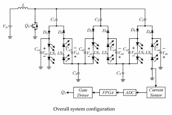
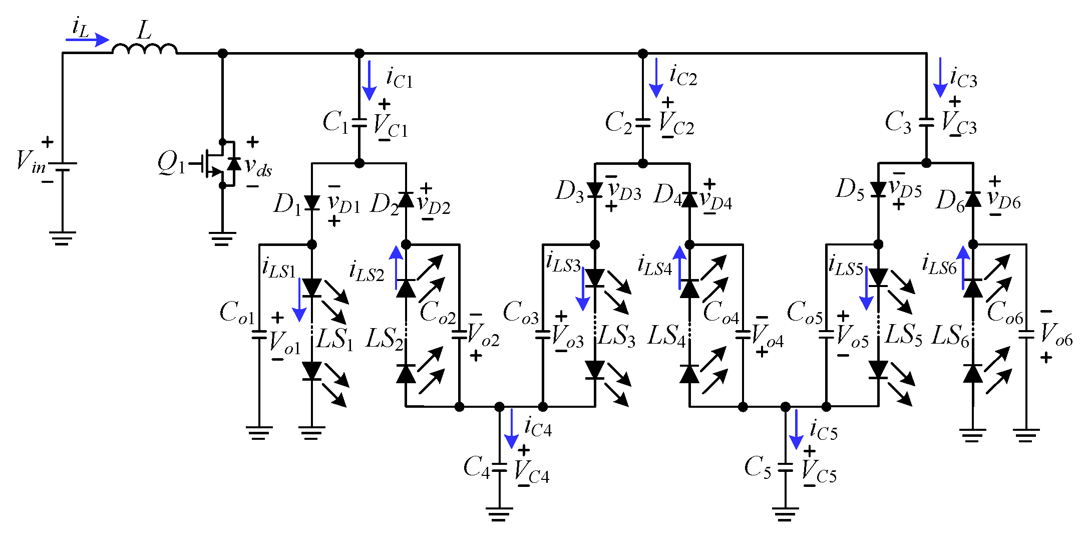
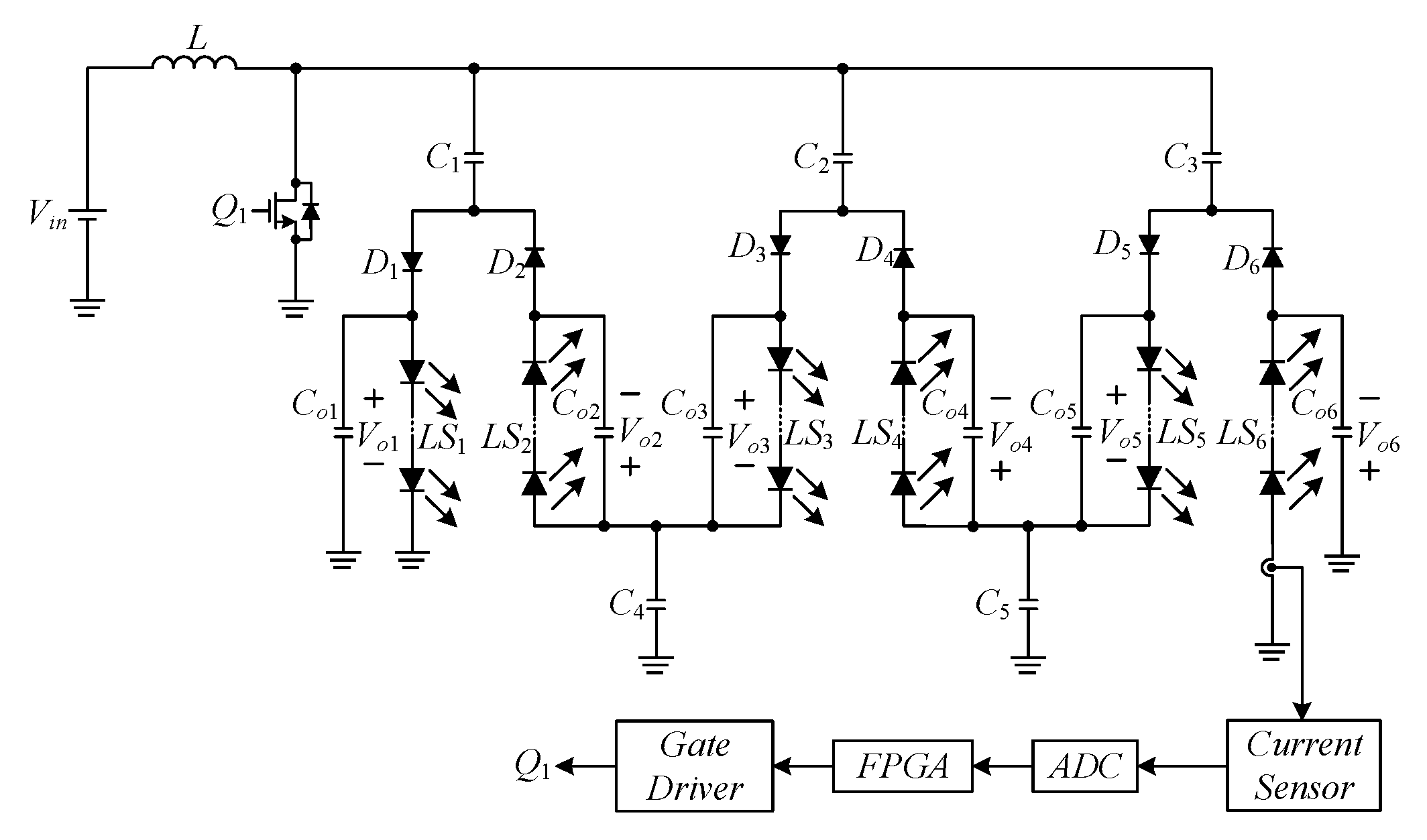
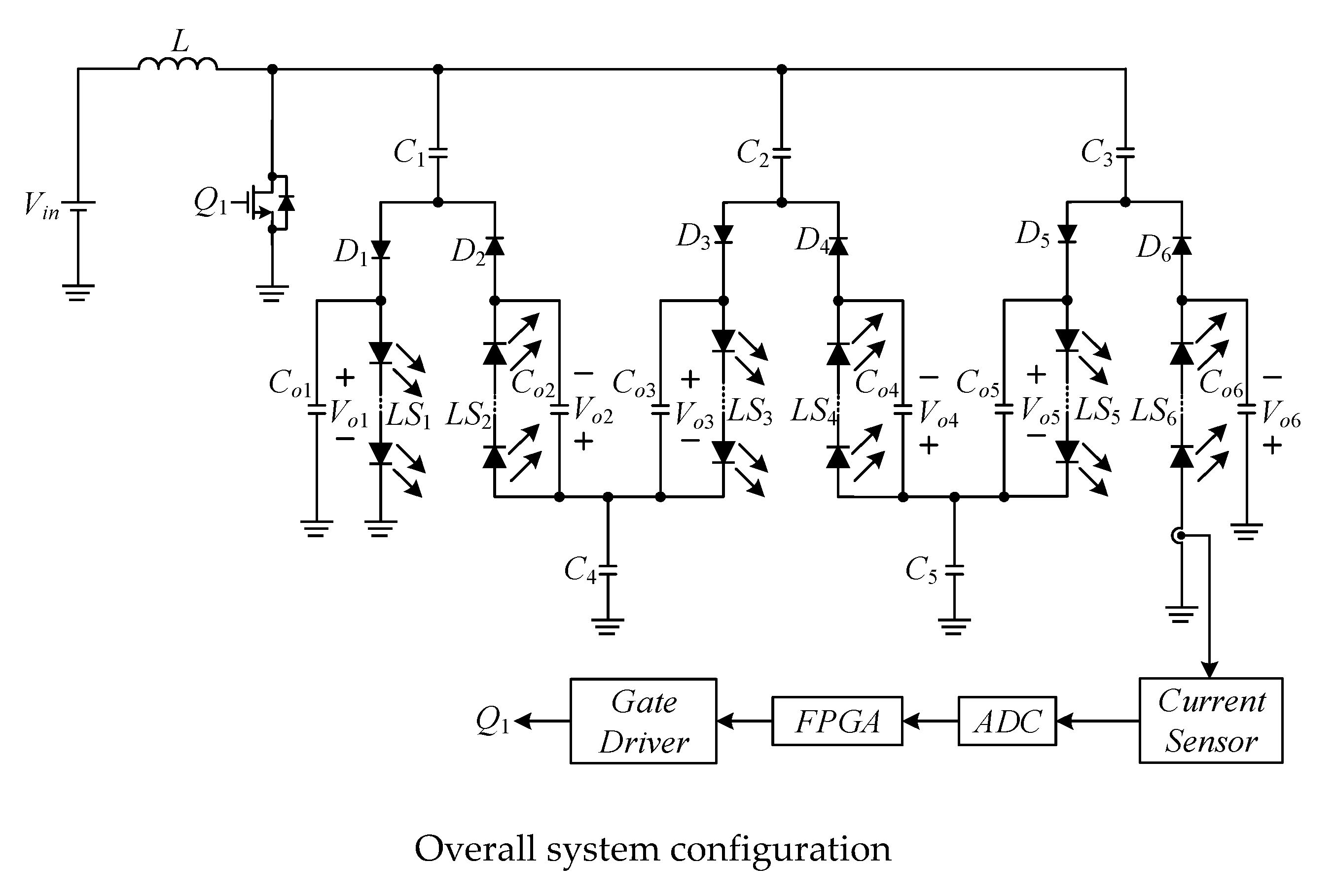
2. Proposed LED Driver Circuit

Since the number of LED strings shown in [18] is four, in order to effectively describe the behavior of the current-sharing interleaved capacitors used in the proposed LED driver, the number of LED strings is set to six. The proposed LED driver circuit in Figure 1 is constructed of one switch, Q1; one input inductor, L; five current-sharing interleaved capacitors, C1, C2, C3, C4, and C5; six diodes, D1, D2, D3, D4, D5, and D6; and six output capacitors Co1, Co2, Co3, Co4, Co5, and Co6. In addition, six LED strings are used as load.
Prior to analysis of the basic operating principle of this circuit, some associated symbols and some assumptions are to be given in the following.
(1)
All the capacitors are large enough such that the voltages across them can be regarded as constant.
(2)
The input voltage is signified by Vin and the output voltages are represented by Vo1, Vo2, Vo3, Vo4, Vo5, and Vo6.
(3)
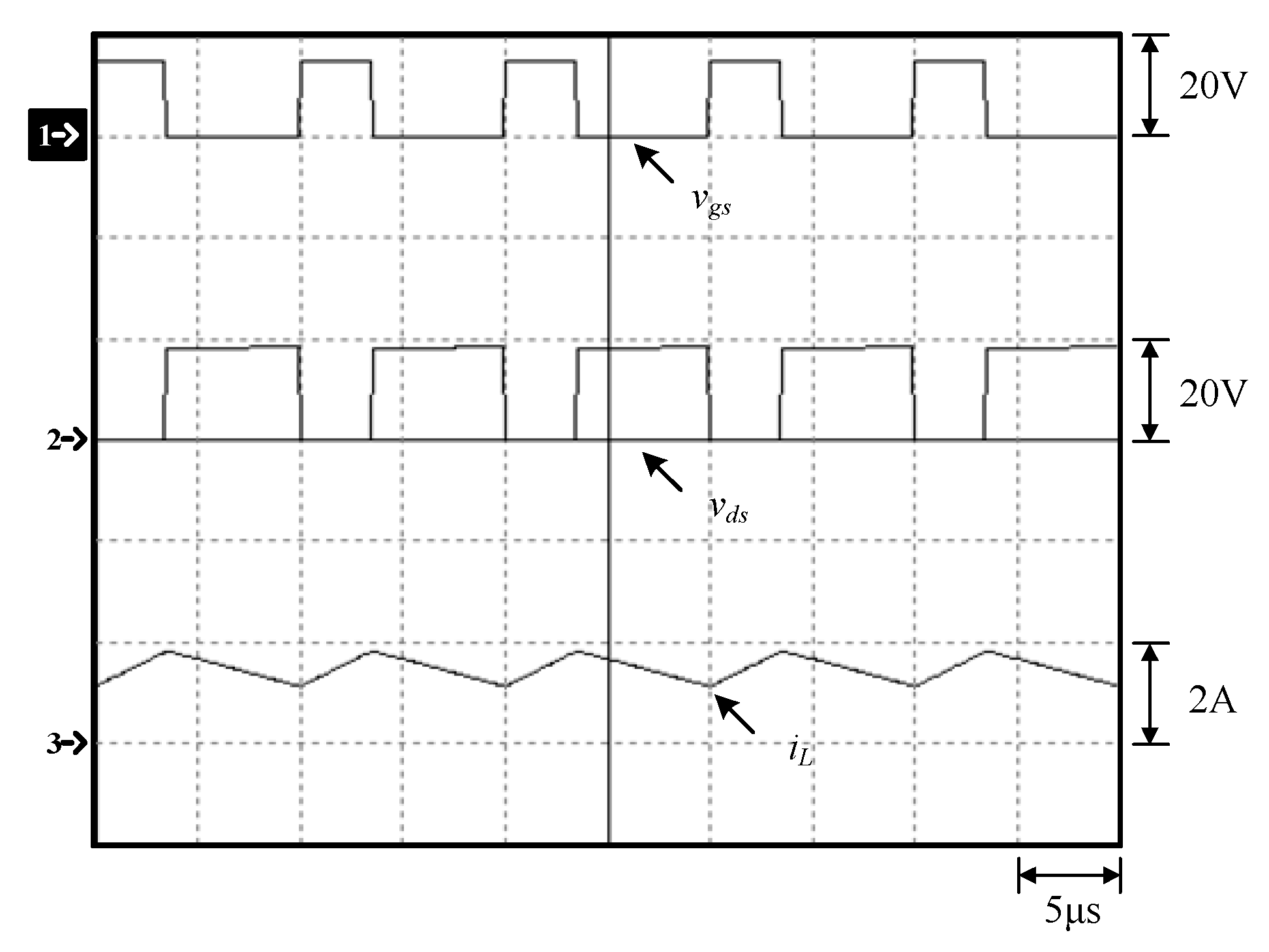
The currents in L and Q1 are indicated by iL and ids, respectively.
(4)
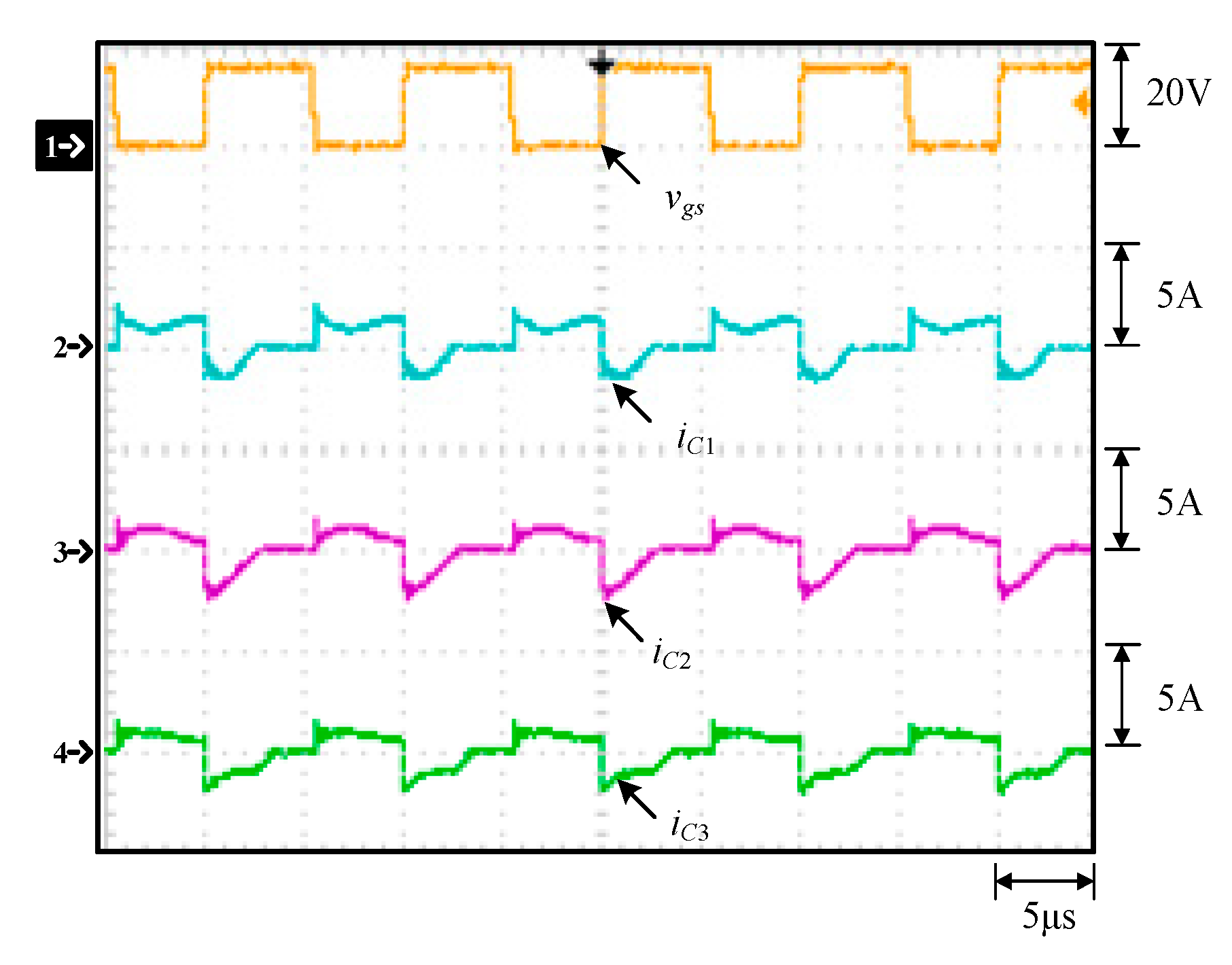
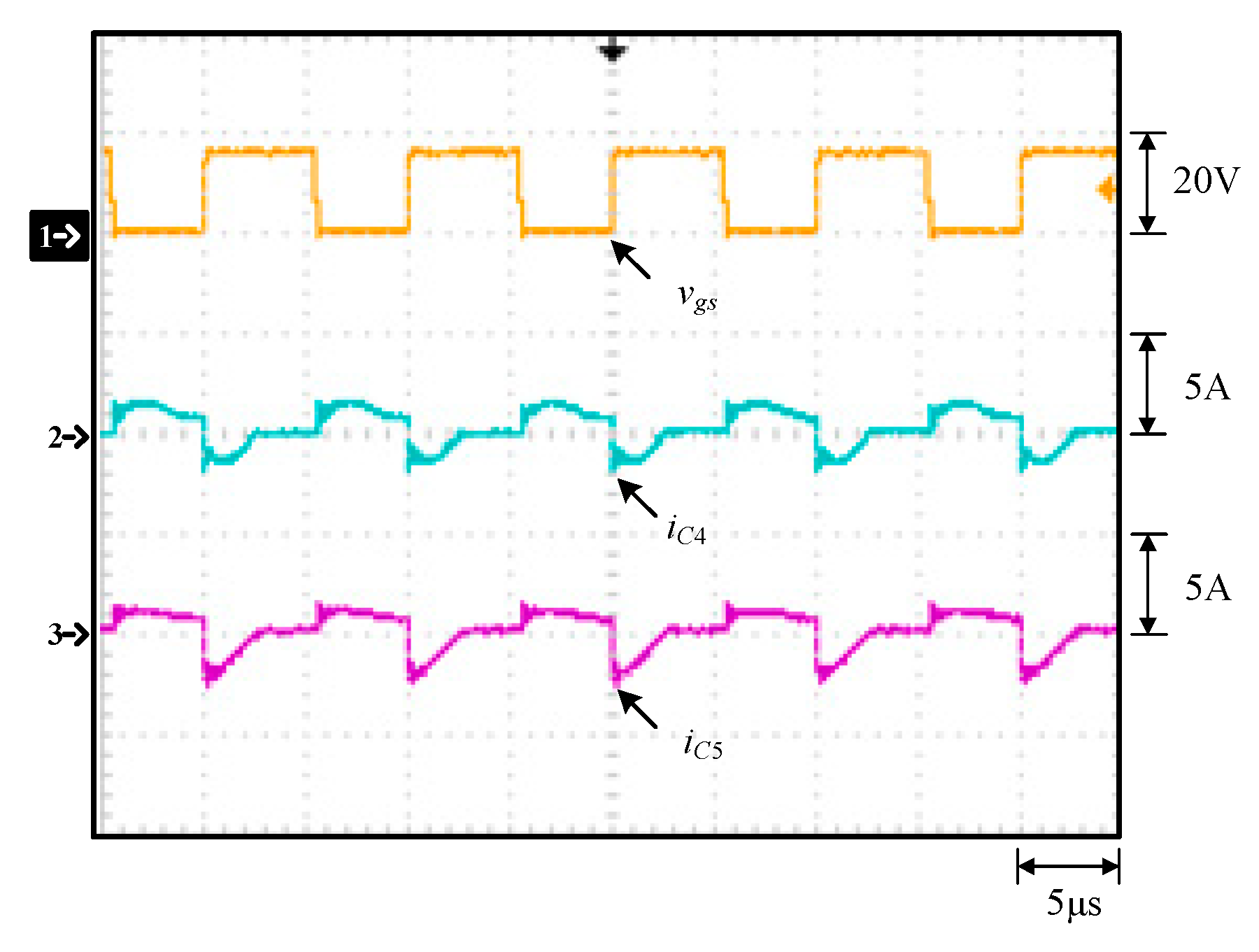
The currents in C1, C2, C3, C4, and C5 are denoted by iC1, iC2, iC3, iC4, and iC5, respectively.
(5)
The currents in Co1, Co2, Co3, Co4, Co5, and Co6 are signified by io1, io2, io3, io4, io5, and io6, respectively.
(6)
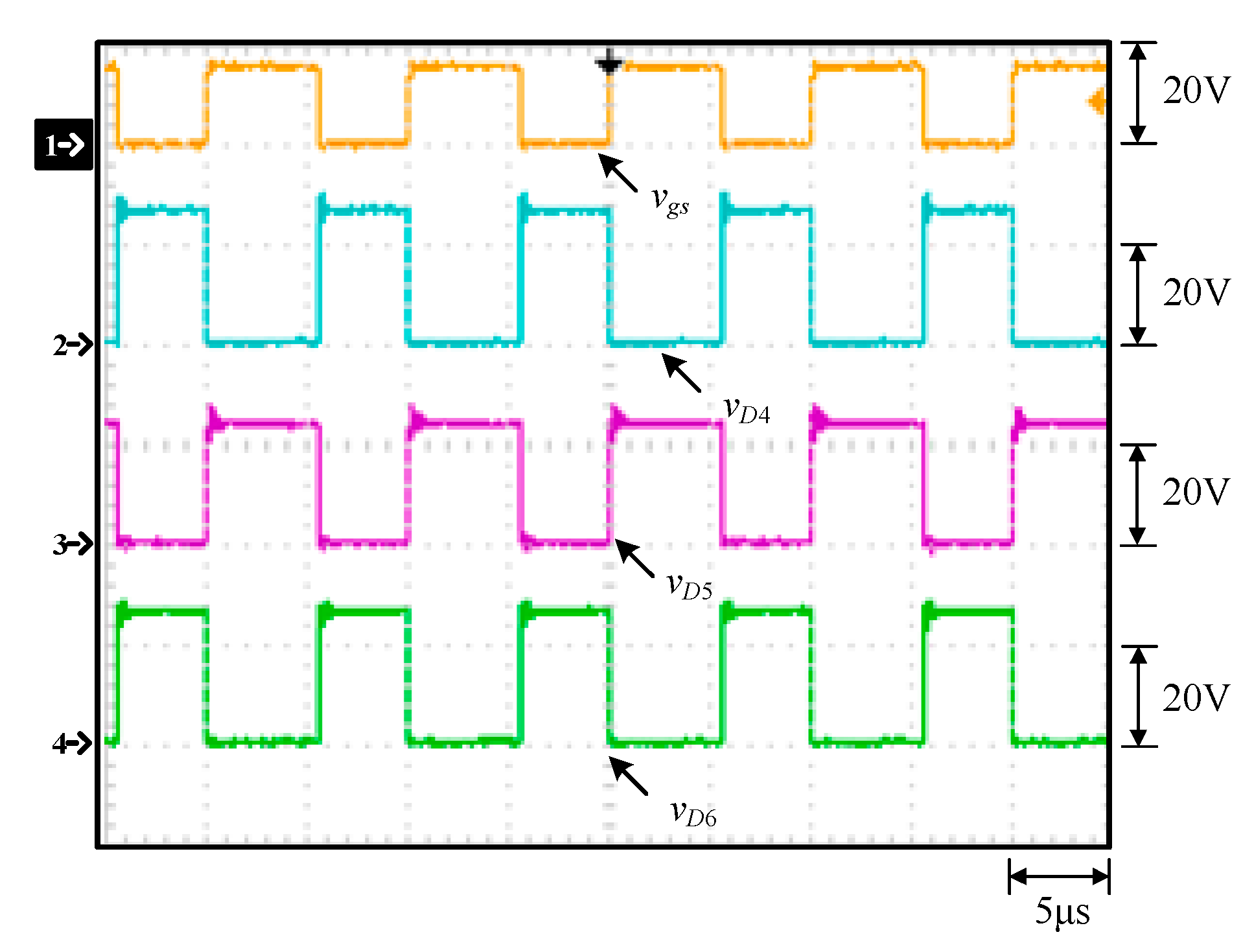
The voltages on L and Q1 are represented by vL and vds, respectively.
(7)
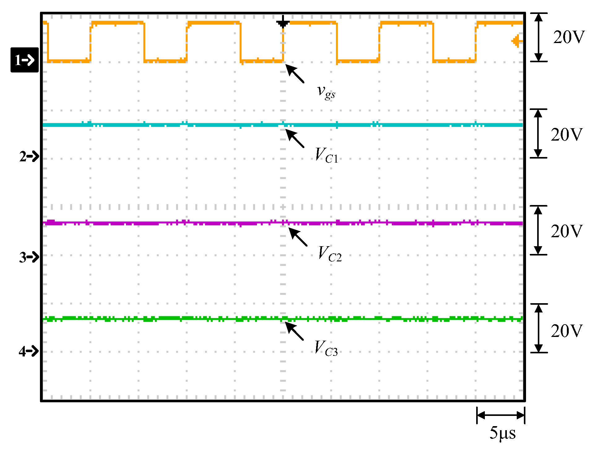
The voltages on C1, C2, C3, C4, and C5 are expressed by VC1, VC2, VC3, VC4, and VC5, respectively.
(8)
The switching period is denoted by Ts.
(9)
The turn-on time interval of Q1 is DTs, where D is the duty cycle.
(10)
The switch, the inductor and all diodes and capacitors are viewed as ideal, and all the LED strings are identical.
(11)
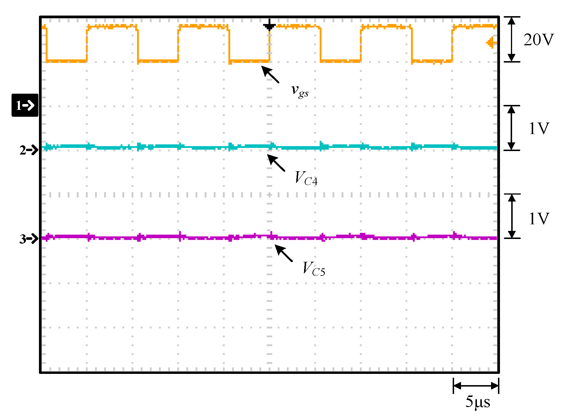
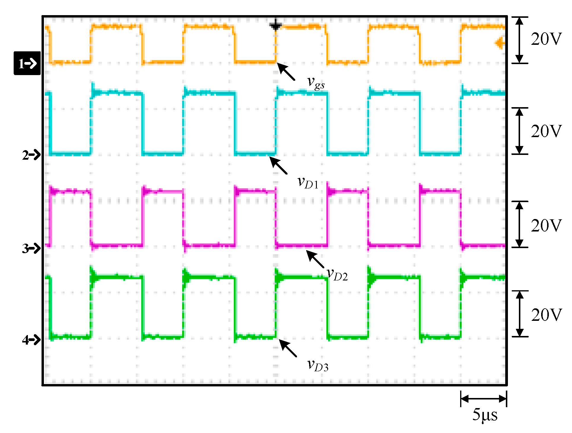
The gate driving signal for Q1 is signified by vgs.
(12)
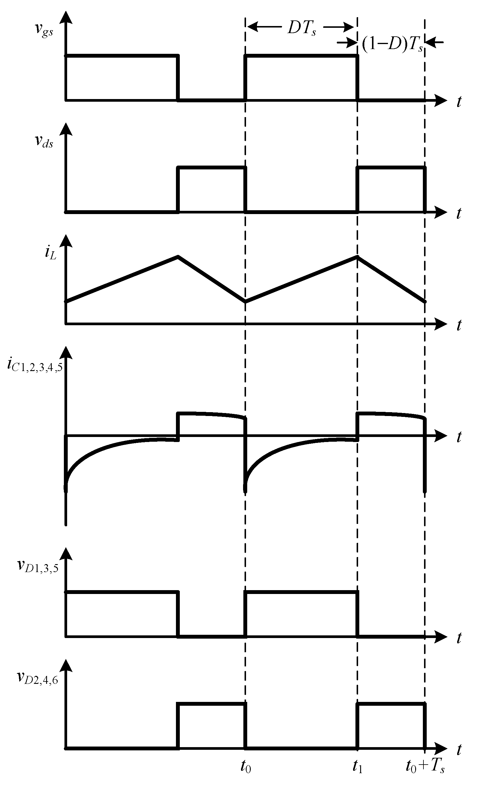
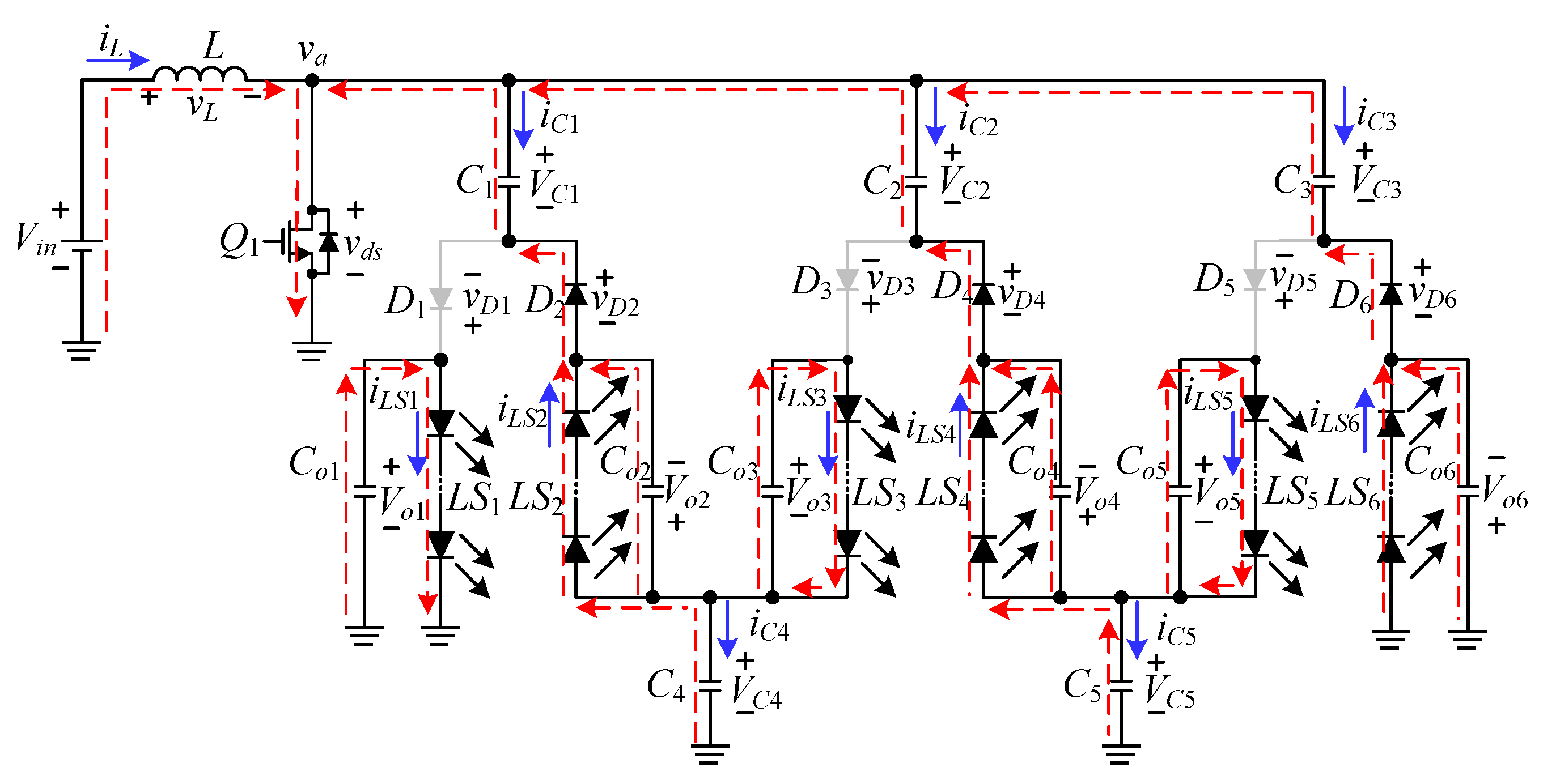
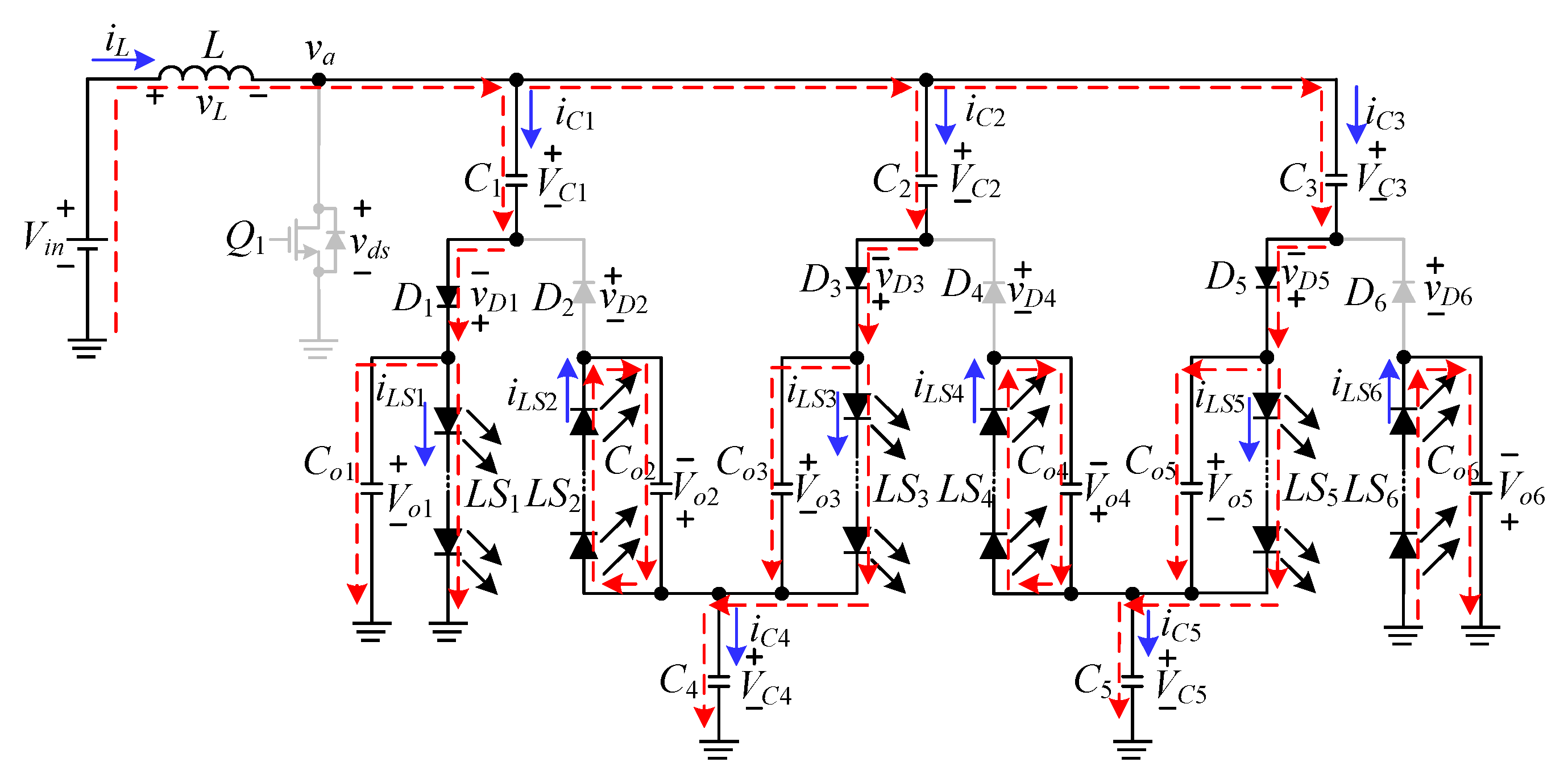
The circuit is operated in the continuous conduction mode (CCM), that is, there are two operating states over one switching cycle, as shown in Figure 2.

2.1. Operating Principle Analysis

(1)
State 1: [ t 0 t t 1 ]: As shown in Figure 3, Q1 is turned on. At the same time, D1, D3, and D5 are turned off, whereas D2, D4, and D6 are turned on. During this state, the voltage across L is Vin, L is magnetized, whereas C1, C2, C3, C4, and C5 are discharged through Q1 and provide energy to LS2, LS4, and LS6 and Co2, Co4, and Co6. In addition, the energy required by LS1, LS3, and LS5 is provided by Co1, Co3, and Co5, respectively.
(2)
State 2: [ t 1 t t 2 ]: As shown in Figure 4, Q1 is turned off. At the same time, D2, D4, and D6 are turned off, whereas D1, D3, and D5 are turned on. During this state, the voltage across L is Vinva, where va = VC1 + Vo1. The inductor L, together with Vin, charges C1, C2, C3, C4, C5, Co1, Co3, and Co5, whereas the energy required by LS2, LS4, and LS6 are provided by Co2, Co4, and Co6, respectively.

2.2. Voltage Gain

As Q1 is turned on, the voltage across L, vL(on), can be expressed as
v L ( o n ) = V i n .
As Q1 is turned off, the voltage across L, vL(off), can be expressed as
v L ( o f f ) = V i n v a .
According to the voltage-second balance over one switching cycle, the following equation can be obtained:
D V i n + ( 1 D ) ( V i n v a ) = 0 .
By rearranging (3), the input voltage Vin can be obtained as
V i n = v a ( 1 D ) .
During the turn-on period of Q1, the following equations can be found:
{ V C 1 + V C 4 V o 2 = 0 V C 2 + V C 5 V o 4 = 0 V C 3 V o 6 = 0 .
During the turn-off period of Q1, the following equations can be found:
{ V C 1 + V o 1 = v a V C 2 + V o 3 + V C 4 = v a V C 3 + V o 5 + V C 5 = v a .
By summing the equations shown in (5), the following equation can be obtained:
V C 1 + V C 2 + V C 3 + V C 4 + V C 5 V o 2 V o 4 V o 6 = 0 .
By summing the equations shown in (6), the following equation can be obtained:
V C 1 + V C 2 + V C 3 + V C 4 + V C 5 + V o 1 + V o 3 + V o 5 = 3 v a .
By subtracting (7) from (8), the voltage va can be obtained as
v a = 1 3 ( V o 1 + V o 2 + V o 3 + V o 4 + V o 5 + V o 6 ) .
Finally, by substituting (9) into (4), the corresponding voltage gain can be found to be
v a V i n = 1 3 m = 1 6 V o m V i n = 1 1 D .
From (10), it can be seen that the required duty cycle is determined by averaging all the voltages across LED strings and then multiplying this result by two. If all the LED strings are identical, then (10) can be simplified to be
v a V i n = 2 V o 1 V i n = 1 1 D .
From (11), it can be seen that the duty cycle can be determined by the output voltage of one LED string. That is, the output voltage and duty cycle of the proposed LED driver are kept constant as the number of LED strings is increased, and Equation (11) still holds.

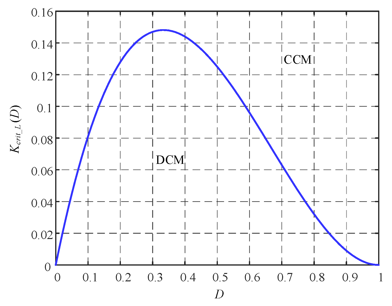
2.3. Boundary Condition of Input Inductor L

The boundary condition for L is described as
{ 2 I L Δ i L L   works   in   the   CCM 2 I L Δ i L L   works   in   the   DCM ,
where IL and ΔiL are DC and AC components of iL.
For analysis convenience, it is assumed that the input power is equal to the output power, and hence, the input current Iin can be represented by
I i n = 1 1 D × V o R e q ,
where Req is the equivalent output resistance.
The average current of iL, IL, can be expressed as
I L = I i n
I L = 1 1 D × V o R e q .
Furthermore, the current ripple of iL, ΔiL, can be represented by
Δ i L = V L Δ t L = V i n D T s L .
Therefore, as 2IL ≥ ΔiL, the input inductor L will operate in the CCM, and hence, the following equation can be obtained:
2 I L Δ i L 2 × 1 1 D × V o R e q V i n D T s L 2 L R e q T s V i n D ( 1 D ) V o 2 L R e q T s ( 1 D ) 2 D K L K c r i t _ L ( D ) ,
where K L = 2 L R e q T s and K c r i t _ L ( D ) = ( 1 D ) 2 D .
From (17), it can be seen that as KL Kcrit_L(D), the input inductor L operates in the CCM; otherwise, in the DCM. Therefore, the operation boundary curve of L can be drawn as shown in Figure 5.

2.4. Current Sharing Concept

For convenience of analysis, only the current-sharing interleaved capacitor C1 is taken into account. According to the ampere-second balance, the absolute value of the electric charge during the turn-on period of Q1, QC1_on, is equal to the electric charge during the turn-off period of Q1, QC1_off; namely,
| Q C 1 _ o f f | = Q C 1 _ o n
1 T s 0 D T s | i C 1 ( o n ) |   d t = 1 T s D T s T s i C 1 ( o f f )   d t .
The current in the LED string LS1 is equal to the absolute average value of the negative part of iC1 during the turn-on period of Q1, and the current in the LED string LS2 is equal to the average value of the positive part of iC1 during the turn-off period of Q1; therefore:
| I C 1 ( o n ) | = I C 1 ( o f f ) = I L S 1 = I L S 2 .

3. System Control Strategy

Figure 6 shows the systems configuration of the proposed LED driver. This system contains the main power stage and the feedback control loop. The main power stage is constructed by the proposed LED driver. As for the feedback control loop, the current in the last LED string is sensed by the current sensor and then sent to the analog-to-digital converter (ADC), which transfers the analog signal to the digital signal. Afterwards, this digital signal is transferred to the field-programmable gate array (FPGA) to get a suitable control force after some calculations, so as to control the switch such that the currents in all the LED strings can be controlled near a desired value.

4. Design Considerations

Prior to tackling this section, the system specifications are given in Table 1 as follows.

4.1. Determination of Duty Cycle

According to the LED V-I curve shown in [22], the forward voltage VF and forward current IF at rated condition are 3.45V and 0.35A, respectively, whereas the cut-in forward voltage VF,LED at zero current is 2.7 V. Hence, the equivalent resistance RF,LED is 2.143 Ω.

4.1.1. Duty Cycles at Rated Load

The maximum duty cycle at rated load, Dmax,rated, is determined by the minimum input voltage Vin,min and is shown as follows:
D m a x , r a t e d = 1 V i n , m i n I L E D × Σ R F , L E D + Σ V F , L E D = 1 10.8 0.35 × 17.14 + 21.6 = 0.608
The minimum duty cycle at rated load, Dmin,rated, is determined by the maximum input voltage Vin,max and is shown as follows:
D m i n , r a t e d = 1 V i n , m a x I L E D × Σ R F , L E D + Σ V F , L E D = 1 13.2 0.35 × 17.14 + 21.6 = 0.522

4.1.2. Duty Cycles at Minimum Load

The maximum duty cycle at minimum load, Dmax,min, is determined by the minimum input voltage Vin,min and is shown as follows:
D m a x , m i n = 1 V i n , m i n 25 % × I L E D × Σ R F , L E D + Σ V F , L E D   = 1 10.8 0.25 × 0.35 × 17.14 + 21.6 = 0.532
Also, the minimum duty cycle at minimum load, Dmin,min, is determined by the maximum input voltage Vin,max and is shown as follows:
D m i n , m i n = 1 V i n , m a x 25 % × I L E D × Σ R F , L E D + Σ V F , L E D = 1 13.2 0.25 × 0.35 × 17.14 + 21.6 = 0.428

4.2. Design of L

In order to make sure that the input inductor L works in the CCM, the minimum average input inductor current IL,min should satisfy the following inequality:
I L , m i n Δ i L 2 ,
where Δ i L is the input inductor current ripple.
Via setting the efficiency equal to one, the following equation can be obtained as
I L , m i n = I i n , m i n = P o , m i n V i n , m a x .
Therefore, the inequality of L can be expressed as
L V i n , m a x D m i n , m i n T s 2 × I L , m i n = V i n , m a x 2 D m i n , m i n T s 2 × P o , m i n = 13.2 2 × 0.428 × 10 μ 2 × 7.25 = 51.36 μ H .
Eventually, the value of L is set at 60 µH.

4.3. Design of Co1–Co6

The values of Co1Co6 are worked out at a rated condition. Since the voltages across the capacitors Co1, Co2, Co3, Co4, Co5, and Co6 are clamped by the identical LED strings, Vo1 = Vo2 = Vo3 = Vo4 = Vo5 = Vo6. Furthermore, the capacitors Co1, Co3, and Co5 are used to provide the energy for LS1, LS3, and LS5 during the turn-on period of Q1, respectively, whereas the capacitors Co2, Co4, and Co6 are used to provide the energy for LS2, LS4, and LS6 during the turn-off period of Q1, respectively. In addition, it is assumed that the voltage ripple for each output capacitor is set at 1% of its DC voltage. Therefore,
C o 1 = C o 3 = C o 5 I o , r a t e d × D m a x , r a t e d × T s V o 1 × 1 %   = 0.35 × 0.608 × 10 μ 13.8 × 0.01 = 15.4 μ F
C o 2 = C o 4 = C o 6 I o , r a t e d × ( 1 D m a x , r a t e d ) × T s V o 2 × 1 %   = 0.35 × ( 1 0.522 ) × 10 μ 13.8 × 0.01 = 12.1 μ F .
Finally, one 22 μF/25 V capacitor is for Co1 and also for Co2, Co3, Co4, Co5, and Co6.

4.4. Design of C1–C5

The values of C1C5 are figured out at rated condition. In this LED driver, the capacitors C1, C2, and C3 have the same operating behavior, namely, VC1 = VC2 = VC3, whereas the capacitors C4 and C5 have the same operating behavior, namely, VC4 = VC5. From state 2 with the switch Q1 being off and based on Kirchhoff’s law (KVL), the following equation can be obtained:
V C 4 V o 3 V C 2 + V C 1 + V o 1 = 0
Hence, VC4 = 0 since VC1 = VC2 and Vo1 = Vo3. In the same way, VC5 = 0.
From state 1 with the switch Q1 being on and based on KVL, the following equation can be obtained:
V C 1 V o 2 + V C 4 = 0 .
Hence, VC1 = Vo2 since VC4 = 0. In the same way, VC2 = Vo4 and VC3 = Vo6.
In addition, it is assumed that the voltage ripple for each capacitor is set at 1% of its DC voltage. Therefore,
C 1 = C 2 = C 3 P o , r a t e d 3 × V i n , m i n × D m a x , r a t e d × T s V o 1 × 1 %   = 29 3 × 10.8 × 0.608 × 10 μ 13.8 × 0.01 = 39.1 μ F
Eventually, one 47 μF/25 V capacitor is for C1 and also for C2 and C3. As for C4 and C5, they have the same capacitances as that for C1 for design convenience.
In the following, the component specifications are tabulated in Table 2.

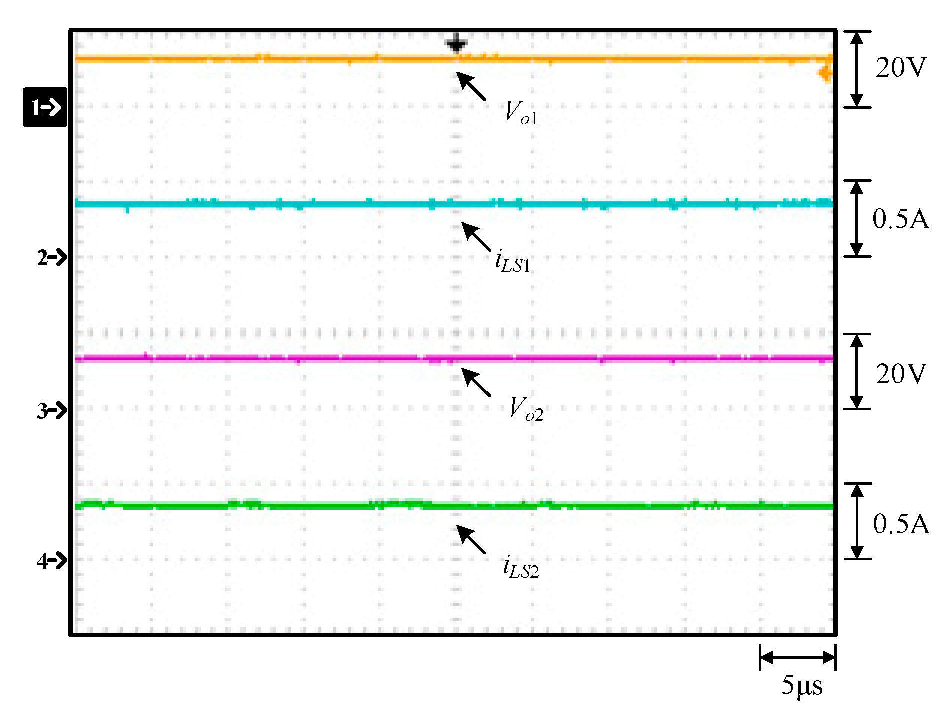
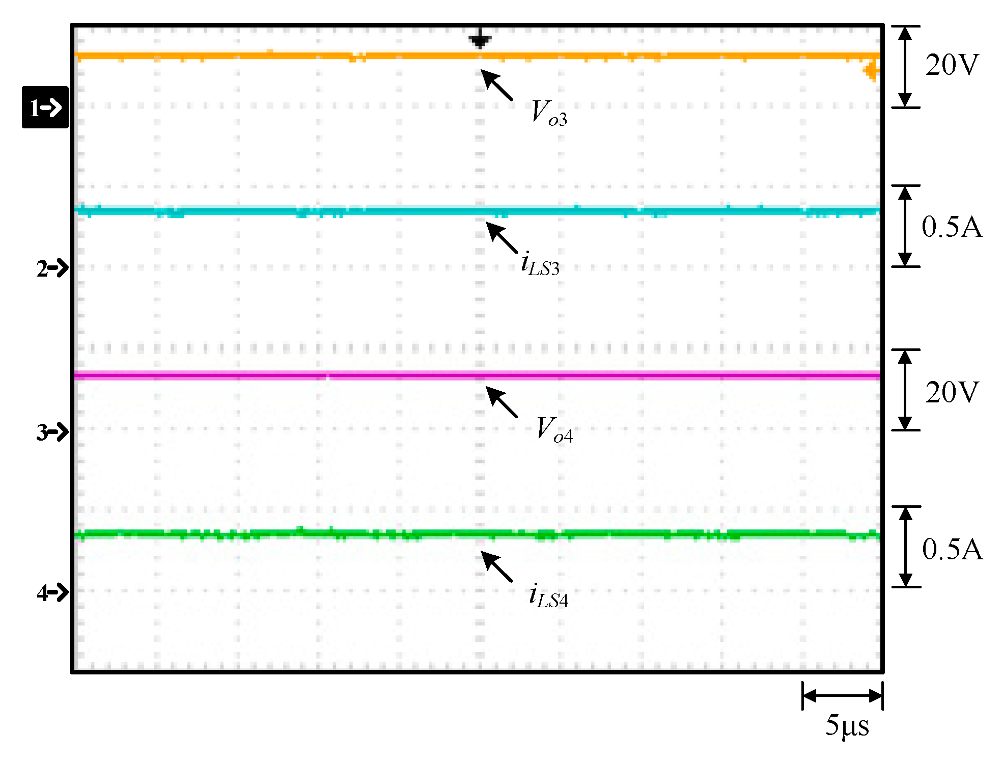
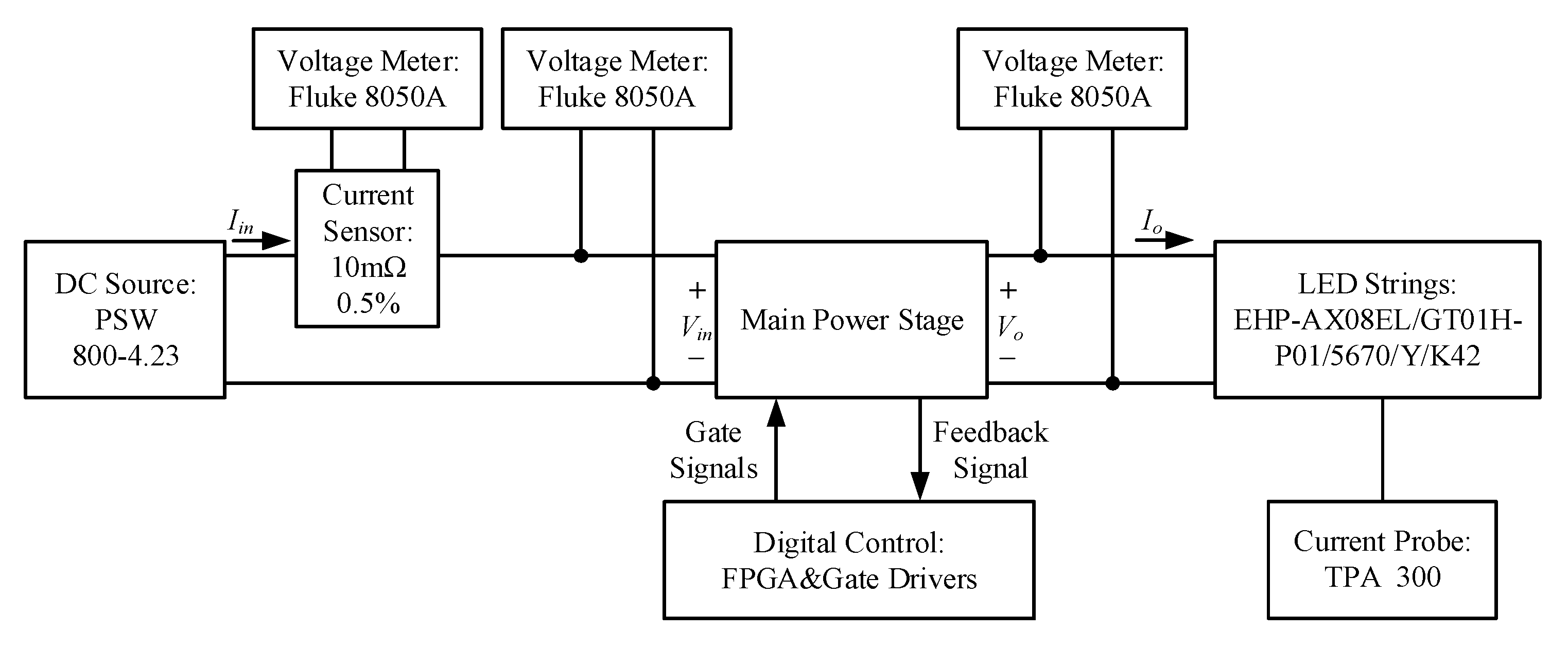
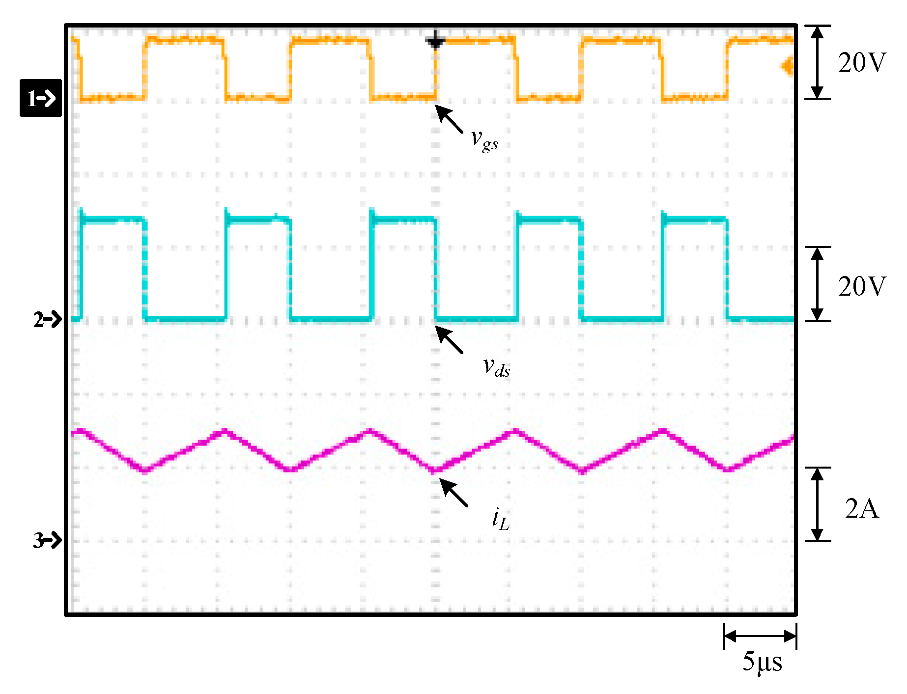
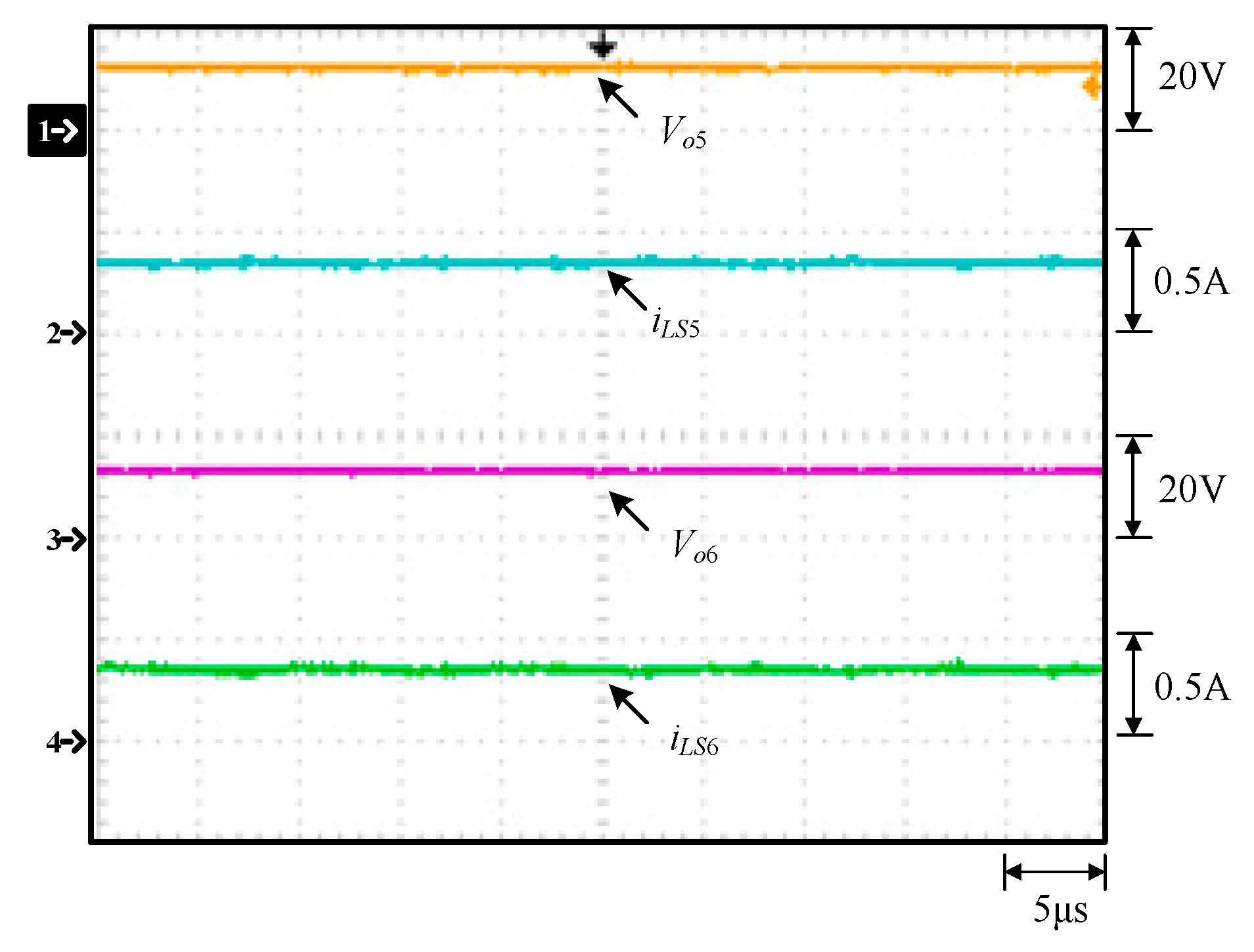
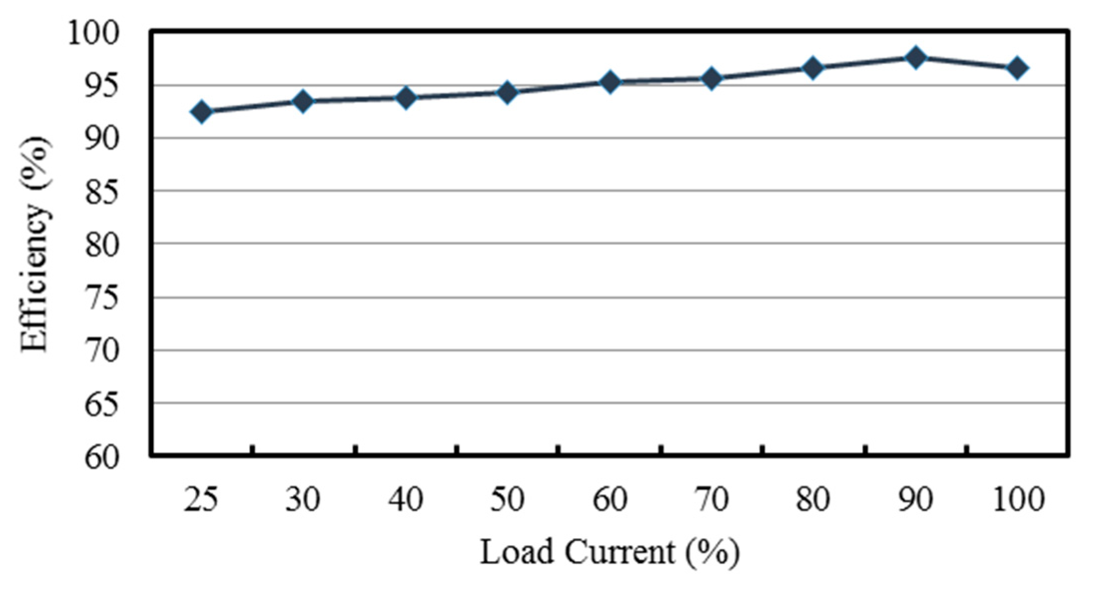
5. Experimental Results

Figure 7, Figure 8, Figure 9, Figure 10, Figure 11, Figure 12 and Figure 13 shows the waveforms related to the proposed LED driver at rated condition. Figure 7 shows the gate driving signal for Q1, vgs, the voltage on Q1, vds, and the current in L. Figure 8 shows the gate driving signal for Q1, vgs, the voltages across C1, C2, and C3, called VC1, VC2, and VC3, respectively. Figure 9 shows the gate driving signal for Q1, vgs, and the voltages across C4 and C5, called VC4 and VC5, respectively. Figure 10 shows the gate driving signal for Q1, vgs, and the voltages across D1, D2, and D3, called vD1, vD2, and vD3, respectively. Figure 11 shows the gate driving signal for Q1, vgs, and the voltages across D4, D5, and D6, called vD4, vD5, and vD6, respectively. Figure 12 shows the gate driving signal for Q1, vgs, and the currents in C1, C2, and C3, called iC1, iC2, and iC3, respectively. Figure 13 shows the gate driving signal for Q1, vgs, and the currents in C4 and C5, called iC4 and iC5, respectively. Figure 14 shows the voltage across LS1, Vo1, the current in LS1, iLS1, the voltage across LS2, Vo2, and the current in LS2, iLS2. Figure 15 shows the voltage across LS3, Vo3, the current in LS3, iLS3, the voltage across LS4, Vo4, and the current in LS4, iLS4. Figure 16 shows the voltage across LS5, Vo5, the current in LS5, iLS5, the voltage across LS6, Vo6, and the current in LS6, iLS6.
From Figure 7, the input inductor L operates in the CCM. From Figure 7, Figure 10 and Figure 11, the voltages across Q1, D2, D4, and D6 have voltage rings during the turn-off transient of Q1, due to resonance among the body capacitance of Q1, the diode parasitic capacitances of D2, D4, and D6, and the line parasitic inductances. From Figure 8, the voltages across C1, C2, and C3 are fixed at some values, whereas from Figure 9, the voltages across C4 and C5 are kept close to zero. From Figure 10 and Figure 11, the voltages across D1, D3, and D5 have voltage rings during the turn-on transient of Q1, due to resonance among the diode parasitic capacitances of D1, D3, and D5, and the line parasitic inductances. From Figure 12 and Figure 13, the currents flowing through C1 to C5 have negative current rings since the voltages across D1, D3, and D5 have voltage rings during the turn-on transient of Q1, whereas the current flowing through C1 to C5 have positive current rings since the voltages across D2, D4, and D6 have voltage rings during the turn-off transient of Q1. From Figure 14, Figure 15 and Figure 16, the current sharing between LEDs performs well, and the corresponding voltages across LS1 to LS6 are almost the same due to all LED strings being almost identical.
In addition, Table 3, Table 4 and Table 5 show the current sharing error percentage (CSEP) under an input voltage of 12 V and different current levels in LED strings. The definition of CSEP is shown as follows:
CSEP y = I L S y ( x = 1 m I L S x ) ÷ m ( x = 1 m I L S x ) ÷ m × 100 %
where CSEPy is the CSEP of the y-th LED string, m is the total number of LED strings, ILSy is the current flowing through the y-th LED string, and x = 1 m I L S x is the sum of all the currents flowing through the LED strings.
Based on the calculated measurements from Table 3, Table 4 and Table 5, the CSEP values for any load locate between −1% and 1%. Therefore, the proposed LED driver has a good capability of current sharing.
In the following, how to measure the efficiency of the proposed LED driver is described. As shown in Figure 17, one current sensing resistor is in series with the input current path. First, a digital meter, called Fluke 8050A, is used to measure the voltage across this resistor so as to obtain the value of the input current. Sequentially, another digital meter, also called Fluke 8050A, is used to measure the input voltage. Accordingly, the input power can be worked out. As for the output power, six LED strings with the same number of LEDs, manufactured by Everlight Lighting Co., are used as the load of this LED driver. At the same time, the voltages across these six LED strings are measured by the other digital meter, also called Fluke 8050A. After this, the currents in these six LED strings are measured by a current probe, named TCPA 300, manufactured by Tektronix Co. Accordingly, the output power can be worked out. Finally, the corresponding efficiency can be figured out based on the calculated input and output powers. Figure 18 shows the curve of efficiency versus load current percentage. From this figure, it can be seen that the efficiency is above 90% all over the load range and can be up to 97.6%.

6. Further Discussion on Current-Sharing Performance

In this section, to further demonstrate the current performance of the proposed LED driver, the number of LEDs for all the LED strings are not identical, e.g., three LEDs for LS1, one LED for LS2, three LEDs for LS3, two LEDs for LS4, four LEDs for LS5, and three LEDs for LS6. The waveforms shown in Figure 19, Figure 20, Figure 21 and Figure 22, based on the PSIM software, are obtained under the rated LED current of 350 mA. Figure 19 shows the gate driving signal for Q1, vgs, the voltage on Q1, vds, and the current in L, iL. Figure 20 shows the voltage across LS1, Vo1, the current in LS1, iLS1, the voltage across LS2, Vo2, and the current in LS2, iLS2. Figure 21 shows the voltage across LS3, Vo3, the current in LS3, iLS3, the voltage across LS4, Vo4, and the current in LS4, iLS4. Figure 22 shows the voltage across LS5, Vo5, the current in LS5, iLS5, the voltage across LS6, Vo6, and the current in LS6, iLS6, since the voltage across each LED is assumed to be 3.45 V at rated current. Accordingly, based on (10), the calculated duty cycle, close to the simulated value shown in Figure 19, is
D = 1 3 m = 1 6 V o m V i n 1 3 m = 1 6 V o m = 18.4 12 18.4 0.35
In addition, from Figure 19, Figure 20, Figure 21 and Figure 22, it can be seen that even though the LED counts for individual LED strings are not the same, the currents flowing through all the LED strings are almost identical due to current control and current-sharing interleaved capacitors.

7. Conclusions

For the circuits shown in the literature [10,11,12,13,14,15,16,17,18,19,20,21], each circuit has the capability of extending the number of LED strings to two or more if necessary, except for [12,20,21]. Since the current balance based on the differential transformer will occupy a relatively large space, the current balance of the proposed LED driver is based on the capacitor. In this paper, an LED driver with extendable parallel structure and automatic current balance is presented. This LED driver is modified from series-type LED strings in [18] to parallel-type LED strings. The output voltage of the proposed LED driver with parallel-type LED strings is determined by averaging all the voltages across LED strings and then multiplying this result by two, different from the LED driver with series-type LED strings shown in [18], the output voltage of which is the sum of all the voltages across LED strings shown in (4) in [18]. Therefore, in [18], the voltage rating of the main switch will be increased, causing the turn-on resistance of the main switch to be increased. In addition, the number of LED strings cannot be increased to more than four. For the proposed LED driver, if all the LED strings are identical, then the output voltage is kept constant as the number of LED strings is increased; if not, then the output voltage is changed slightly. Moreover, only one current sensor is required to realize current control and dimming.

Author Contributions

The conception was presented by K.-I.H., who also was responsible for editing this paper. Y.-K.T. surveyed the existing papers and wrote the software program. H.-H.T. carried out experimental setup and verification. K.-I.H. was in charge of project administration.

Funding

This research was funded by the Ministry of Science and Technology, Taiwan, under the Grant Number: MOST 108-2221-E-027-051.

Acknowledgments

The authors gratefully acknowledge the support of the Ministry of Science and Technology, Taiwan, under the Grant Number MOST 108-2221-E-027-051.

Conflicts of Interest

The authors declare no conflict of interest.

Nomenclature

Q1Main switch
C1, C2, C3, C4, C5Current-sharing interleaved capacitors
LInput inductor
D1, D2, D3, D4, D5, D6Diodes
Co1, Co2, Co3, Co4, Co5, Co6Output capacitors
LS1, LS2, LS3, LS4, LS5, LS6LED strings
TsSwitching period
fsSwitching frequency
DDuty cycle
t0, t1Time instants
ReqEquivalent output resistance
vgsGate driving signal for Q1
vds, vaVoltage across Q1
idsCurrent in Q1
VC1, VC2, VC3, VC4, VC5Voltages across C1, C2, C3, C4, C5
iC1, iC2, iC3, iC4, iC5Currents in C1, C2, C3, C4, C5
iC1(on)Current iC1 during turn-on period of Q1
iC1(off)Current iC1 during turn-off period of Q1
IC1(on)Constant value of iC1 during turn-on period
IC1(off)Constant value of iC1 during turn-off period
vLVoltage across L
vL(on)Voltage across L during turn-on period of Q1
vL(off)Voltage across L during turn-off period of Q1
iLCurrent in L
IL,minMinimum DC value of iL
∆iLPeak-to-peak value of current ripple of iL
vD1, vD2, vD3, vD4, vD5, vD6Voltages across D1, D2, D3, D4, D5, D6
iD1, iD2, iD3, iD4, iD5, iD6Currents in D1, D2, D3, D4, D5, D6
iLS1, iLS2, iLS3, iLS4, iLS5, iLS6Currents in LS1, LS2, LS3, LS4, LS5, LS6
ILS1, ILS2Dc values of iLS1, iLS2
VinInput voltage
Vin,maxMaximum input voltage
Vin,minMinimum input voltage
VoOutput voltage
Vo1, Vo2, Vo3, Vo4, Vo5, Vo6Voltages across Co1, Co2, Co3, Co4, Co5, Co6
iCo1, iCo2, iCo3, iCo4, iCo5, iCo6Currents in Co1, Co2, Co3, Co4, Co5, Co6
IinInput current
Iin,minMinimum input current
Io,ratedLED rated current
Io,minLED minimum current
Po,minMinimum output power
Po,ratedRated output power
Dmax,ratedMaximum duty cycle at rated load
Dmin,ratedMinimum duty cycle at rated load
Dmax,minMaximum duty cycle at minimum load
Dmin,minMinimum duty cycle at minimum load
QC1_onElectric charge in C1 during turn-on period
QC1_offElectric charge in C1 during turn-off period
VFLED forward voltage
VF,LEDLED forward cut-in voltage
RF,LEDLED resistance
ILEDLED dc current
ILSxDc current in the x-th LED string
ILSyDc current in the y-th LED string
CSEPyy-th CSEPy

References

  1. Narendran, N.; Gu, Y. Life of LED-based white light sources. IEEE J. Disp. Technol. 2005, 1, 167–171. [Google Scholar] [CrossRef]
  2. Sinnadurai, R.; Ahamed, K.M.K.A.; Azri, M.; Vikneswaran. Development of white LED down light for indoor lighting. In Proceedings of the IEEE STUDENT’12, Kuala Lumpur, Malaysia, 6–9 October 2012. [Google Scholar]
  3. Steigerwald, D.A.; Bhat, J.C.; Collins, D.; Fletcher, R.M.; Holcomb, M.O.; Ludowise, M.J.; Martin, P.S.; Rudaz, S.L. Illumination with solid state lighting technology. IEEE J. Sel. Top. Quantum Electron. 2002, 8, 310–320. [Google Scholar] [CrossRef]
  4. Qu, X.; Wong, S.C.; Tse, C.K. Color control system for RGB LED light sources using junction temperature measurement. In Proceedings of the IEEE IECON’07, Taipei, Taiwan, 5–8 November 2007. [Google Scholar]
  5. Chiub, C.-L.; Chen, K.-H. A high accuracy current-balanced control technique for LED backlight. In Proceedings of the IEEE PESC’08, Rhodes, Greece, 15–19 June 2008. [Google Scholar]
  6. Yu, W.; Lai, J.-S.; Ma, H.; Zheng, C. High-efficiency dc-dc converter with twin bus for dimmable LED lighting. IEEE Trans. Power Electron. 2011, 26, 2095–2100. [Google Scholar] [CrossRef]
  7. Lohaus, L.; Liao, L.; Strache, S.; Wunderlich, R.; Heinen, S. Energy efficient current control technique for driving high power LEDs. In Proceedings of the VDE PRIME’12, Aachen, Germany, 12–15 June 2012. [Google Scholar]
  8. Li, S.N.; Zhong, W.X.; Chen, W.; Hui, S.Y.R. Novel self-configurable current-mirror techniques for reducing current imbalance in parallel light-emitting diode (LED) strings. IEEE Trans. Power Electron. 2012, 27, 2153–2162. [Google Scholar] [CrossRef]
  9. Li, Y.-C.; Chen, C.-L. A novel primary-side regulation scheme for single-stage high-power-factor ac-dc LED driving circuit. IEEE Trans. Ind. Electron. 2013, 60, 4978–4986. [Google Scholar] [CrossRef]
  10. Hwu, K.I.; Tu, W.C.; Hon, M.J. A dimmable LED driver based on current balancing transformer with magnetizing energy recycling considered. IEEE J. Disp. Technol. 2014, 10, 388–395. [Google Scholar] [CrossRef]
  11. Zhang, R.; Chung, H.S.-H. Use of daisy-chained transformers for current-balancing multiple LED strings. IEEE Trans. Power Electron. 2014, 29, 1418–1433. [Google Scholar] [CrossRef]
  12. Lin, Y.-L.; Chiu, H.-J.; Lo, Y.-K.; Leng, C.-M. Light-emitting diode driver with a combined energy transfer inductor for current balancing control. IET Power Electron. 2015, 8, 1834–1843. [Google Scholar] [CrossRef]
  13. Zhang, R.; Chung, H.S.-H. Capacitor-isolated multistring LED driver with daisy-chained transformers. IEEE Trans. Power Electron. 2015, 30, 3860–3875. [Google Scholar] [CrossRef]
  14. Hwu, K.I.; Jiang, W.Z.; Hsiao, C.W. Dimmable LED driver based on twin-bus converter and differential-mode transformer. IEEE J. Disp. Technol. 2016, 12, 1122–1129. [Google Scholar] [CrossRef]
  15. Qu, X.; Wong, S.C.; Tse, C.K. An improved LCLC current-source-output multistring LED driver with capacitive current balancing. IEEE Trans. Power Electron. 2015, 30, 5783–5791. [Google Scholar] [CrossRef]
  16. Hwu, K.I.; Jiang, W.Z.; Chen, W.H. Automatic current-sharing extendable two-channel LED driver with non-pulsating input current and zero dc flux. Int. J. Circuit Theory Appl. 2018, 46, 1462–1484. [Google Scholar] [CrossRef]
  17. Chen, X.; Huang, D.; Li, Q.; Lee, F.C. Multichannel LED driver with CLL resonant converter. IEEE J. Emerg. Sel. Top. Power Electron. 2015, 3, 589–598. [Google Scholar] [CrossRef]
  18. Ye, Y.; Cheng, K.W.E.; Lin, J.; Wang, D. Single-switch multichannel current-balancing LED drive circuits based on optimized SC techniques. IEEE Trans. Ind. Electron. 2015, 62, 4761–4768. [Google Scholar] [CrossRef]
  19. Hwu, K.I.; Jiang, W.Z. Nonisolated two-channel LED driver with automatic current balance and zero voltage switching. IEEE Trans. Power Electron. 2016, 31, 8359–8370. [Google Scholar] [CrossRef]
  20. Hwu, K.I.; Jiang, W.Z. Input-current-ripple-free two-channel LED driver. IEEE Trans. Ind. Electron. 2017, 64, 5865–5874. [Google Scholar] [CrossRef]
  21. Hwu, K.I.; Jiang, W.Z. Single-switch coupled-inductor-based two-channel LED driver with a passive regenerative snubber. IEEE Trans. Power Electron. 2017, 32, 4482–4490. [Google Scholar] [CrossRef]
  22. EHP-AX08EL/GT01H-P01/5670/Y/K42 High Power LED-1W Datasheet; Everlight Electronics Co., Ltd.: New Taipei, Taiwan, 2011.
Figure 1. Proposed LED driver.
Applsci 09 05177 g001
Figure 2. Proposed LED driver.
Applsci 09 05177 g002
Figure 3. Circuit operating behavior of state 1.
Applsci 09 05177 g003
Figure 4. Circuit operating behavior of state 2.
Applsci 09 05177 g004
Figure 5. Operation boundary curve of the input inductor L.
Applsci 09 05177 g005
Figure 6. System block diagram of the proposed circuit.
Applsci 09 05177 g006
Figure 7. Measured waveforms at rated load: (1) vgs; (2) vds; (3) iL.
Applsci 09 05177 g007
Figure 8. Measured waveforms at rated load: (1) vgs; (2) VC1; (3) VC2; (4) VC3.
Applsci 09 05177 g008
Figure 9. Measured waveforms at rated load: (1) vgs; (2) VC4; (3) VC5.
Applsci 09 05177 g009
Figure 10. Measured waveforms at rated load: (1) vgs; (2) vD1; (3) vD2; (4) vD3.
Applsci 09 05177 g010
Figure 11. Measured waveforms at rated load: (1) vgs; (2) vD4; (3) vD5; (4) vD6.
Applsci 09 05177 g011
Figure 12. Measured waveforms at rated load: (1) vgs; (2) iC1; (3) iC2; (4) iC3.
Applsci 09 05177 g012
Figure 13. Measured waveforms at rated load: (1) vgs; (2) iC4; (3) iC5.
Applsci 09 05177 g013
Figure 14. Measured waveforms at rated load: (1) Vo1; (2) iLS1; (3) Vo2; (4) iLS2.
Applsci 09 05177 g014
Figure 15. Measured waveforms at rated load: (1) Vo3; (2) iLS3; (3) Vo4; (4) iLS4.
Applsci 09 05177 g015
Figure 16. Measured waveforms at rated load: (1) Vo5; (2) iLS5; (3) Vo6; (4) iLS6.
Applsci 09 05177 g016
Figure 17. Block diagram for efficiency measurement.
Applsci 09 05177 g017
Figure 18. Curve of efficiency versus load current percentage.
Applsci 09 05177 g018
Figure 19. Simulated waveforms at rated load with LED counts being not all the same: (1) vgs; (2) vds; (3) iL.
Applsci 09 05177 g019
Figure 20. Simulated waveforms at rated load with LED counts being not all the same: (1) Vo1; (2) iLS1; (3) Vo2; (4) iLS2.
Applsci 09 05177 g020
Figure 21. Simulated waveforms at rated load with LED counts being not all the same: (1) Vo3; (2) iLS3; (3) Vo4; (4) iLS4.
Applsci 09 05177 g021
Figure 22. Simulated waveforms at rated load with LED counts being not all the same: (1) Vo5; (2) iLS5; (3) Vo6; (4) iLS6.
Applsci 09 05177 g022
Table 1. System specifications.
Circuit Operating ModeCCM
Input voltage (Vin) 12 ± 10 %
Output voltage (Vo) 27.6 V ( = 8 × 3.45 V )
LED Rated current (Io,rated)/Rated Power (Po,rated)350 mA/29 W
LED Minimum current (Io,min)/ Min. Power (Po,min)87.5 mA/7.25 W
Switching frequency (fs)/Period (Ts)100 kHz/10 µs
LED forward voltage (VF) and current (IF) at rated condition3.45 V/0.35 A
LED cut-in forward voltage (VF,LED) at zero current2.7 V
LED strings6 strings with 4 LEDs per string
Table 2. Component specifications.
ComponentsSpecifications
MOSFET: Q1IRF3250Z
Diodes: D1, D2, D3, D4, D5, D6STPS30L60C
Current Sharing Capacitors: C1, C2, C3, C4, C522 µF/25 V
Output Capacitors: Co1, Co2, Co3, Co4, Co5, Co647 µF/25 V
InductorCore: T106-18B, L = 60 µH
Gate DriverTC4420
Table 3. Associated current sharing error percentage (CSEP) measurements at minimum load.
LS1LS2LS3LS4LS5LS6
ILS (mA)85.48685.286.685.386.5
VLED (V)10.711.410.611.510.611.5
Error (%)−0.50.2−0.730.9−0.620.78
Table 4. Associated CSEP measurements at half load.
LS1LS2LS3LS4LS5LS6
ILS (mA)172175172175172175
VLED (V)11.312.111.212.111.212.2
Error (%)−0.860.86−0.860.86−0.860.86
Table 5. Associated CSEP measurements at rated load.
LS1LS2LS3LS4LS5LS6
ILS (mA)348352348347349351
VLED (V)12.41312.313.212.313
Error (%)−0.330.81−0.33−0.62−0.040.53

