Abstract
The laser processing method has proven to produce surfaces while ensuring a low secondary electron yield of oxygen-free high-conductivity copper (OFHC) samples, making it attractive for electron cloud mitigation in next-generation particle accelerators and neutron tubes. In this work, the laser processing method is proposed to OFHC targets for the first time, aiming to reduce the secondary electrons in the neutron tube. The secondary electron yields (SEYs) and the thermal conductivities of Ti film and quaternary Ti–Zr–V–Hf films with unprocessed and laser processed OFHC substrates are investigated. Our results highlight that the thermal conductivity of Ti film with laser processed OFHC substrates is in proximity to the cleaned bare OFHC sample, especially at high temperatures. Moreover, the SEY of coated OFHC substrates are higher than that of coated laser processed substrates, which indicates the better secondary electron suppression capability of coated laser processed substrates. Therefore, the thermal conductivity and SEY results illustrate that the application of Ti and Ti–Zr–V–Hf coated laser processed OFHC can be considered to improve the neutron yield in neutron tubes in the future.
1. Introduction
Sealed neutron tubes are widely used in neutron logging, neutron radiography, the cargo security system of ports, airports, and stations due to the advantages of safety, miniaturization, portability, good tightness [1,2,3], etc. For the sake of improving the nuclear reaction efficiency and reducing the size of neutron tubes, several methods were adopted, for example, the secondary electrons suppression [4], the deuterium or tritium absorption capabilities enhancement [5], and vacuum stability promotion [6].
The suppression of secondary electrons will benefit the reduction of the power and current on the target and the alleviation of the power load, thus improving the heat dissipation capability of the target and the stability of neutron tubes [7]. Several methods have been utilized in neutron tubes for the purpose of secondary electron suppression, including the Faraday cup, magnetic field mitigation, applying biased voltage between the accelerator electrode and the target, introduction of resistance, and the combination of the Faraday cup with the biased voltage method [8]. The main disadvantage of these methods is that they occupy the space of the neutron tube. In addition, some of these methods, such as the Faraday cup method, actually exhibit inadequate secondary electron suppression effects. The laser processing method proposed by Reza et al. [9] is a novel way for the secondary electron suppression, having the benefits of not needing to introduce additional components, low cost, etc. In this work, laser processed oxygen-free high-conductivity copper (OFHC) is proposed to mitigate the secondary electron emission.
Ti film coating is traditionally used in the sealed neutron tubes to absorb hydrogen and its isotopic molecules [10]. Ti film can store hydrogen isotopes steadily with high capacity at room temperature via the formation of metal hydrides, e.g., titanium and hydrogen isotopes, to adsorb more deuterium or tritium on the target. Consequently, Ti film coating can provide sufficient reaction materials for nuclear reactions [11]. To further improve the nuclear reaction efficiency and working stability of neutron tubes, it is necessary to develop a novel film coating for the neutron target. Malyshev et al. put forward that Ti–Zr–V–Hf film coatings have the lowest activation temperature (~140 °C) and higher pumping speed and capacity for H2 than previous binary and ternary alloys film coating getters [12,13,14]. From the perspective of maintaining the vacuum stability in a long-running process, Ti film as a kind of essential getter is usually applied in the neutron tubes. However, there is no report on the application of novel quaternary Ti–Zr–V–Hf non-evaporable getter film coatings in sealed neutron tubes. On the other hand, the thermal conductivity of the Ti–Zr–V–Hf film coated substrate is a key factor which can affect the overall heat transfer performance of the target and the operating life of neutron tubes. Thus, the thermal conductivities of Ti–Zr–V–Hf film will be investigated and compared to the Ti film with laser-treated and untreated OFHC substrates in this work.
The working temperature of the neutron target is usually over 150 °C [15,16] so the deuterium gas absorbed in the film can desorb on the film surface of the target. This kind of desorption can reduce the energy loss of D+ and consequently improve the nuclear reaction and neutron yield. To improve the neutron beam quality, enhance the operating life, and reduce the volume of neutron tubes further, the combination of the laser processing method and the single metal and quaternary alloy film coatings is proposed in this paper for the first time. Quaternary Ti–Zr–V–Hf coating with a lower activated temperature of ~150 °C is proposed to be applied in neutron tubes to improve the hydrogen/deuterium/tritium pumping property. The secondary electron yields, surface morphologies, surface chemistry, and thermal conductivities of Ti film and Ti–Zr–V–Hf film coatings with untreated OFHC and laser processed OFHC substrates were investigated and analyzed.
2. Experiments and Methods
2.1. Sample Preparation
Laser processing was carried out to produce nano/micro structures on the surface of OFHC by a line hatched pattern, with a laser spot of 15 μm, a pitch spacing of 15 μm, a laser power of 16 W, and a scanning speed of 20 mm s−1. After laser processing, treated OFHC samples with a size of 10 mm × 10 mm × 0.5 mm were cleaned in absolute ethyl alcohol and acetone for 15 min, respectively. Then Ti and Ti–Zr–V–Hf films were deposited on these untreated OFHC and laser processed OFHC substrates by the direct current (DC) magnetron sputtering method. The details of the samples in this work are shown in Table 1. Specifically, after laser processing sample #1 was taken for secondary electron yields (SEY) measurement without ultrasonic cleaning.

Table 1.
Sample information in this study.
2.2. Film Deposition
The background pressure and working pressure during film deposition was ~5.8 × 10⁻⁴ Pa and 0.5 Pa, respectively. The discharge power during film deposition was 300 W, with the Ar gas flow of 20 Sccm. For the deposition of Ti–V–Hf–Zr film, Ti–V–Hf–Zr quaternary alloy targets were used in this work, as the Ti–V–Hf–Zr film prepared by alloy targets has been reported to have higher pumping sticking probability and capacity than that prepared by twisted wire targets [13].
2.3. Characterization Method
Here, the thickness of OFHC substrates used for thermal conductivity measurements was 2.5 mm, with diameters of 12.7 mm. The specific heat and thermal diffusivity were measured by a NETZSCH LFA 467 Hyper Flash system from 25 °C to 300 °C, with the acquisition rates of the temperature sensor at 2 MHz. To increase the absorptivity and emissivity of the sample, graphite was coated on both sides of the sample before thermal conductivity measurements. Thermal conductivity (W m−1 K−1), λ, of the sample can be calculated via the following equation:
where is the thermal diffusivity (mm2 s−1), is the specific heat capacity (J g−1 K−1), and is the bulk density (g cm−3). The density of the sample was measured by Archimedes’ method. The thermal diffusivity accuracy of NETZSCH LFA was about ±3%. The accuracy of thermal conductivity was around ±5%, which was influenced by the accuracy of thermal diffusivity, specific heat capacity, and bulk density.
The surface microstructures were investigated by A JEOL 7800F Schottky field scanning electron microscopy (SEM). Surface roughness characteristics of the samples were obtained using LEXT Olympus OLS4000-SU laser scanning confocal microscopy (LSCM). The Brunauer–Emmett–Teller (BET) surface areas of the laser treated and untreated OFHC before and after film deposition were analyzed by a BELSORP-Max instrument (MicrotracBEL, Osaka, Japan). The samples were outgassed at 383 K for 6 h in the vacuum. The surface chemical properties of the samples were determined via an AXIS Ultrabld X-ray photoelectron spectroscopy (XPS) with monochromatized Al Ka Xray source. The SEY properties were characterized under normal incidence using a dedicated SEY measurement device which was introduced in Reference [17]. The electron dose for SEY tests was about 7 × 10⁻⁶ C cm−2, with an electron beam spot size of ~1 mm.
3. Results and Discussion
3.1. SEM and XPS Results
In the neutron tube, the Ti film thickness on the target is generally larger than 1 μm [18,19]. This is because the mean free path of D+ is about 0.75–1.03 μm for energy of primary D+, varying between 100 keV and 150 keV. In this work, the film coating thickness with untreated OFHC substrates was 2.20 μm, as shown in Figure 1.
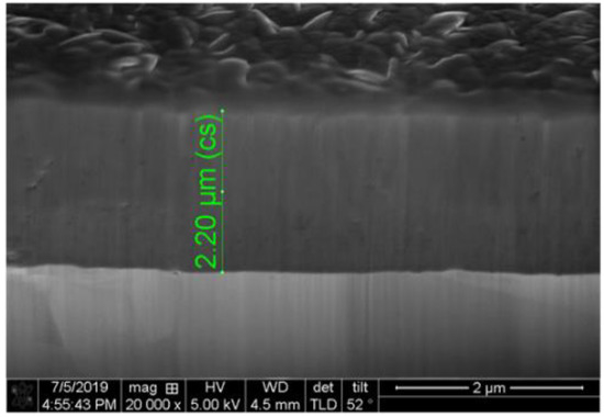
Figure 1.
FIB-SEM (Focused Ion beam-scanning electron microscope) fracture morphology of Ti film coating with untreated oxygen-free high-conductivity copper (OFHC) substrate.
Generally, surface topography could influence the SEY of the samples. Rougher surfaces may contribute to the decrease of SEY [20]. Thus, SEM topographies of laser treated and untreated OFHC samples before and after film depositions were investigated.
The SEM micrographs with 30,000×, 10,000× and 1000× magnification of Ti-Zr-V-Hf film with SEM micrographs with cleaned laser processed OFHC substrates are shown in Figure 2. The SEM microstructures of these two kinds of films deposited on the untreated and cleaned laser treated OFHC substrates are analyzed, as shown in Figure 2 and Figure 3.
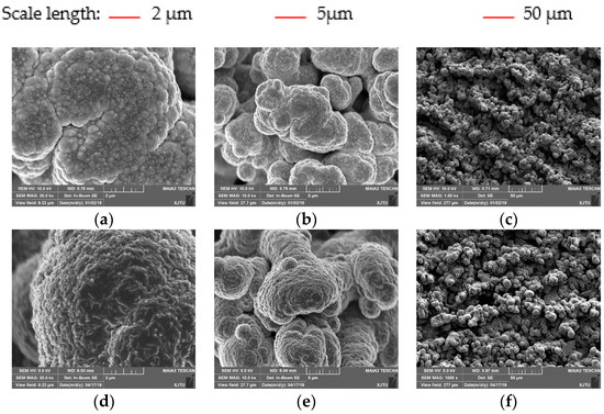
Figure 2.
The SEM (Scanning electron microscope) micrographs of the Ti–Zr–V–Hf and Ti film coatings with cleaned laser processed OFHC substrates. (a–c) are the SEM images of Ti–Zr–V–Hf film coatings. (d–f) are the SEM images of Ti film coatings.
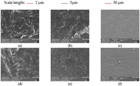
Figure 3.
The SEM (Scanning electron microscope) micrographs of the Ti and Ti–Zr–V–Hf film coatings with cleaned OFHC substrates at different scales. Here, (a–c) are the SEM micrographs of Ti–Zr–V–Hf film coatings. (d–f) are the SEM micrographs of Ti film coatings.
The surface of Ti and Ti–Zr–V–Hf films with cleaned laser processed OFHC substrates was obviously rougher than the ones with cleaned OFHC substrates. The specific surface area of cleaned OFHC was 1.74 m2/g. Moreover, the specific surface areas of the Ti and Ti–Zr–V–Hf coated cleaned laser processed OFHC substrates were 4.42 m2/g and 4.93 m2/g, respectively, and that of Ti and Ti–Zr–V–Hf coated cleaned OFHC substrates were 2.41 m2/g and 2.52 m2/g, respectively. Thus, the specific surface area results were basically in accord with the SEM results.
The rougher surface contributed to the SEY decrease of Ti and Ti–Zr–V–Hf films with cleaned laser processed OFHC substrates in contrast to the ones with untreated substrates. The grain size of Ti–Zr–V–Hf film was smaller than the one of Ti film. The morphologies of Ti–Zr–V–Hf and Ti film coatings with cleaned laser processed OFHC substrates indicate the presence of sphere/island-like structures entrenched within uneven pores. For Ti film, this kind of sphere/island-like structures comprise tens of nanometer-sized, sphere-like grains with sizes ranging from 20 to 100 nm.
Figure 2a and Figure 3a reveal that the grains of Ti-Zr-V-Hf film are globular-like structures, while the ones of Ti film in Figure 2d are squamous-like structures. The difference in grain structures may be caused by the sputtered target atoms. When the view field is 27.7 μm, the surface textures of Ti-Zr-V-Hf and Ti film coatings showed in Figure 2b,e are columnar-like structures. It can be speculated that the curves formed after laser processing play an essential role in microstructural evolution during film deposition. Rougher film coating surfaces were obtained with laser processed OFHC substrates, which contribute to the SEY reduction of Ti-Zr-V-Hf and Ti film coatings.
The surface average roughnesses (Ra) of bare OFHC and laser treated OFHC were 0.189 μm and 7.143 μm, respectively. As shown in Table 1, the surface roughnesses of Ti film and Ti–Zr–V–Hf film on bare OFHC substrates were 0.110 μm and 0.131 μm, respectively. When the substrates were cleaned laser treated OFHC, the surface roughnesses of Ti film and Ti–Zr–V–Hf film were 6.842 μm and 6.902 μm, respectively. It can be concluded that the surface roughnesses of film-coated substrates decreased slightly compared to that of uncoated ones. Moreover, the surface roughnesses of Ti–Zr–V–Hf films were slightly higher than that of Ti films, but lower than that of the substrates.
Figure 3 shows the surface morphologies of Ti–Zr–V–Hf and Ti film coatings with cleaned OFHC substrates. It was observed that Ti–Zr–V–Hf film with cleaned OFHC substrate in Figure 3c was denser than the one with cleaned laser processed OFHC substrate in Figure 2c. The same principle appeared to Ti films with cleaned, untreated, and laser processed OFHC substrates. This may be attributed to the SEY decrease of Ti films with cleaned laser processed substrate. Several researchers reported that a rough surface could suppress secondary electron emission (SEE) dramatically [21,22,23,24,25,26]. Despite the increased emitting surface area induced by laser processing which favors SEE, a portion of the SEE can be absorbed by the surface protrusions. The balancing effect is the partial mitigation of SEE by absorption, to some extent resting with the surface morphology formed by laser processing, thus synthesizing micro-structured surfaces with a high possibility to acquire low SEY surface.
As shown in Figure 4, the XPS survey spectra indicate that the ratio of Ti, Zr, V, and Hf elements is around 2.4:2.6:1.0:1.2. It is worth noting that O and C are the two main contaminants for Ti film and Ti–Zr–V–Hf film coatings. This can be explained because C and O elements were introduced during air exposure and sample transfer.
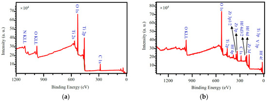
Figure 4.
The X-ray photoelectron spectroscopy (XPS) survey spectra for the surfaces of (a) Ti film and (b) Ti–Zr–V–Hf quaternary alloy film coatings.
3.2. SEY Results
The SEY properties of laser processed OFHC, Ti film, and Ti–Zr–V–Hf film coatings with OFHC and laser processed OFHC substrates are shown in Figure 5. When the primary electron energy varied between 100 and 3000 eV, the maximum SEYs (δmax) of Ti film coating and Ti–Zr–V–Hf film coatings with OFHC substrates were 1.49 and 1.37, respectively, with the corresponding primary energy (Emax) of 200 and 300 eV, respectively. The δmax of Ti and Ti–Zr–V–Hf film coatings with laser processed OFHC substrates were 1.34 and 1.18, respectively. The δmax of as-received OFHC samples were 1.6–2.0 [19,21,22] with different polish states and SEY test parameters. It can be seen that the δmax of Ti and Ti–Zr–V–Hf film coatings with laser processed OFHC substrates are lower than the ones of as-received OFHC samples.
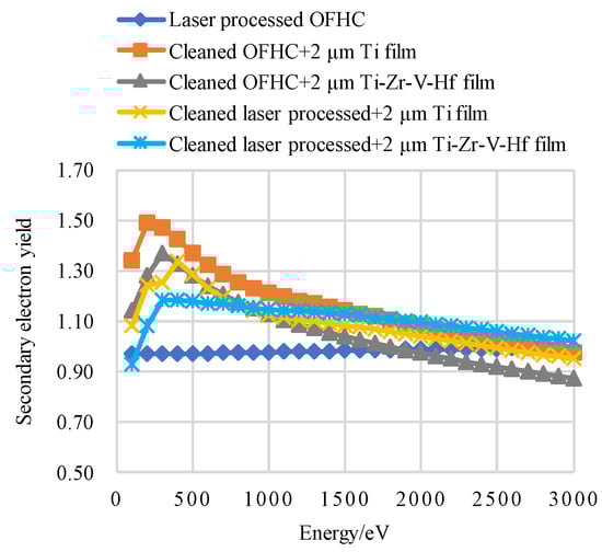
Figure 5.
The secondary electron yield (SEY) of laser processed OFHC, Ti film, and Ti–Zr–V–Hf coated laser processed OFHC substrates.
Compared to the δmax of laser processed OFHC, the ones with Ti film coating and Ti–Zr–V–Hf film coating with laser processed OFHC increased from 0.99 to 1.34 and 1.18, respectively. The SEY increase of Ti film coating and Ti–Zr–V–Hf film coating may relate to the sizes of the particles and grains on the surface, and the existence of nano-size floccules formed by laser processing, etc. In other words, the reduction of floccules-like structures formed by laser ablation and the increase of grain size after film deposition may have contributed to the SEY increase of both films. When the substrate was bare OFHC, the δmax of Ti film coating and Ti–Zr–V–Hf film coating were 1.49 and 1.37, respectively. These results indicate that the δmax of Ti-Zr-V-Hf quaternary alloy film coatings with bare OFHC is slightly lower than the one of Ti film coating with the same substrate. This can possibly be explained because the lower δmax property of Ti–Zr–V–Hf film may be determined by the surface morphologies and physical properties of film coatings, etc.
3.3. Thermal Conductivity Results
When the test temperature range varies between 25 and 300 °C, the effect of radiation heat transfer can be neglected. Moreover, considering heat loss, the Cowan+ impulse correction was adopted. Figure 6 displays the thermal conductivities of cleaned bare OFHC, Ti films, and Ti–Zr–V–Hf films with untreated OFHC and laser processed OFHC in the test temperature ranging from 25 to 300 °C. It can be seen that the thermal conductivities of all the samples decreased gradually with the increase of temperature. The thermal conductivities of the cleaned bare OFHC sample vary between 417.7 W m−1 K−1 and 382.3 W m−1 K−1 in the temperature range of 25–300 °C, which are consistent with reported values [27,28,29,30,31]. For the films deposited on the untreated OFHC substrate, the thermal conductivities of Ti films were 3.3%–10.2% higher than the Ti–Zr–V–Hf films at the same temperatures. In comparison, the thermal conductivities of Ti films on the laser processed OFHC were 6.3%–20.1% higher than the Ti–Zr–V–Hf films with the same substrates. Additionally, the thermal conductivity differences between Ti and Ti–Zr–V–Hf films increased gently with the increase of test temperature.
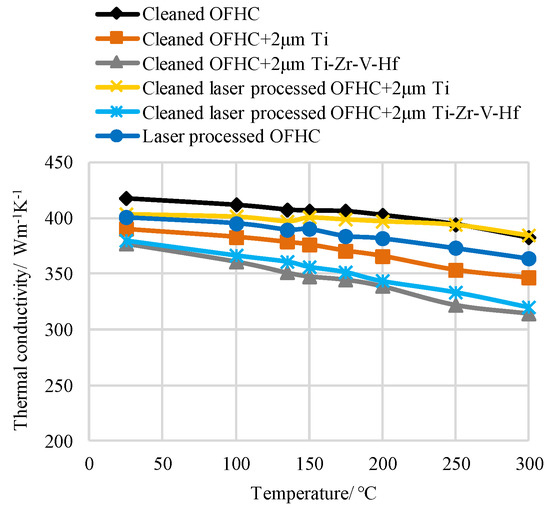
Figure 6.
The thermal conductivities of laser processed OFHC, Ti film, and Ti–Zr–V–Hf coated laser processed OFHC substrates.
When the substrates are the same, the thermal conductivities of Ti films are higher than the ones of Ti–Zr–V–Hf quaternary alloy films. The structural disorder degree of Ti–Zr–V–Hf films are higher than that of Ti film, which may contribute to the thermal conductivity difference [27,32,33,34]. In addition to the film composition, the laser processing also influences the thermal conductivity but the roles are complicated. Laser processing treatment significantly reduces the thermal conductivity of the bare cleaned OFHC. However, in the presence of coatings, laser processing on the OFHC substrate becomes beneficial.
Figure 6 shows that the thermal conductivities of Ti films with cleaned laser processed OFHC substrates are higher than the ones with cleaned OFHC substrates. In particular, when the test temperatures are 250 and 300 °C, respectively, the thermal conductivities of cleaned OFHC and Ti films with cleaned laser processed OFHC substrates are very close. Concurrently, the thermal conductivities of Ti films with cleaned laser processed OFHC substrates are higher than the ones with cleaned OFHC substrates. However, the thermal conductivities of Ti–Zr–V–Hf films with cleaned untreated OFHC and laser processed OFHC substrates are equivalent to a certain degree.
Interface bonding plays a pivotal role in the thermal conductivities of Ti and quaternary alloy Ti–Zr–V–Hf films with cleaned OFHC substrates. The mechanism of the effect of interface bonding on thermal conductivity has been reported by other scholars [35]. Higher disorder degree results in low thermal conductivities for the quaternary alloy with respect to Ti film. The results confirm that cleaned laser processed OFHC substrates coated with Ti has a positive effect on the thermal properties compared with Ti film on cleaned OFHC substrates. It can be speculated that the interface bonding of Ti film with cleaned OFHC substrates is worse than the one with cleaned laser processed OFHC substrates. This can be attributed to the thermal conductivity increase of Ti film with cleaned laser processed OFHC substrates. Nevertheless, the disorder degree of Ti film is lower than the one of Ti–Zr–V–Hf film. The coupling effect of interface bonding and disorder degree results in the thermal conductivity difference for Ti and quaternary alloy Ti–Zr–V–Hf films with different kinds of OFHC substrates. In other words, the porous layer is formed on the surface of the substrate after laser processing, which can induce thermal conductivity reduction to some extent. However, the porous structure interface with film coating may improve the thermal conductivity of coated laser processed samples.
After laser processing, the surface areas of as-received OFHC substrates increased with respect to untreated ones. The increased surface areas can effectively flatten the power density distribution for neutron tubes. For single metal Ti films, the laser processing technique can improve the thermal conductivities by 3.5%–11.5% as shown in Figure 6. Laser processing can reduce the thermal conductivities of film coatings at a certain degree, while film deposition can improve the thermal conductivities of film coatings, especially at high test temperatures. It can be explained that the surface porous structures formed by laser processing were filled by coatings which benefit the improvement of thermal conductivity.
The hydrogen pumping property of Ti–Zr–V–Hf film is better than the one of Ti film as reported by Malyshev et al. [13,36]. Theoretically, the deuterium and tritium pumping properties of Ti–Zr–V–Hf film are superior to the ones of Ti film [37]. Hence, combined with the laser processing method, the Ti–Zr–V–Hf film with laser processed OFHC substrates may improve the neutron yield in neutron tubes effectively. The validity and related mechanism of Ti–Zr–V–Hf film with laser processing OFHC targets in neutron tubes requires further systematic study.
4. Conclusions
In conclusion, the thermal conductivity of Ti film with cleaned laser processed OFHC substrates was 3.5%–11.5% higher than the one with as-received OFHC substrates. Moreover, the δmax of Ti film with cleaned laser processed OFHC substrates was lower than the one with untreated cleaned OFHC substrates, when the energy of the primary electrons varies between 100 eV and 3000 eV. By comparing the thermal conductivity of Ti film with laser treated and untreated OFHC substrates, we have found that the laser processed technique is an effective way to improve the thermal conductivity and reduce the SEY of Ti film. Secondly, the thermal conductivity of Ti film cleaned laser processed OFHC is very close to the one of the cleaned OFHC, especially at a high test temperature (200–300 °C). The thermal conductivity of laser processed OFHC may be related to the thickness of film coatings and laser parameters, such as laser power, pitch spacing, etc. For the application of the laser ablation method in the neutron tube, high thermal conductivity and low SEY properties are preferable. Finally, based on the experimental results on SEY and thermal conductivity, the application of the laser processed method to obtain low SEY and a high thermal conductivity surface should be considered in target surface treatment of neutron tubes in the future.
Author Contributions
Conceptualization, J.W. and S.G.; methodology, Z.Y., J.F. and J.Z.; validation, J.W., Y.G. and S.Y.; investigation, J.W. and Y.G.; data curation, J.W., Y.G., Z.Y., J.F., J.Z. and S.Y.; writing—original draft preparation, J.W.; writing—review and editing, J.W., S.W., S.G. and Z.X.; supervision, S.W. and Z.X.; funding acquisition, S.W. and Z.X.
Funding
This research was funded by the key project of Intergovernmental International Scientific and Technological Innovation Cooperation in China under Grant No. 2016YFE0128900, China Postdoctoral Science Foundation Grant No. 2018M643667, the National Natural Science Foundation for the Youth of China No. 11905170, the Fundamental Research Funds for the Central Universities No. XJH012019018, Shaanxi Province Postdoctoral Science Foundation Grant No. 2018104, the Fundamental Research Funds for the Central Universities No. XJH012019011, and the National Natural Science Foundation of China under Grant No.11775166.
Acknowledgments
We would like to thank Shengli Wu and Jie Li from Institute of Physical Electronics and Devices of Xi’an Jiaotong University for their help with SEY tests. We would like to also thank Jiamei Liu at Instrument Analysis Center of Xi’an Jiaotong University for her assistance with XPS tests.
Conflicts of Interest
The authors declare no conflict of interest.
References
- Yurkov, D.I.; Dulatov, A.K.; Lemeshko, B.D.; Golikov, A.V.; Andreev, D.A.; Mikhailov, Y.V.; Selifanov, A.N. Pulsed neutron generators based on the sealed chambers of plasma focus design with D and DT fillings. J. Phys. Conf. Ser. 2015, 653, 012019. [Google Scholar] [CrossRef]
- Xiaohui, M.; Zhiwei, D. The dynamic study on the influence of secondary electrons on ion beam quality. High Power Laser Part. Beams 2018, 30, 114005. [Google Scholar]
- Rashchikov, V.I.; Shikanov, A.E. Compact plasma reflex triode for neutron generation. IEEE T. Plasma Sci. 2019, 47, 1279–1282. [Google Scholar] [CrossRef]
- Jianlin, K.; Meng, L.; Changgeng, Z. Deuteron induced secondary electron emission from titanium deuteride surface. Nucl. Instrum. Meth. B 2012, 280, 1–4. [Google Scholar] [CrossRef]
- Falabella, S.; Tang, V.; Ellsworth, J.L.; Mintz, J.M. Protective over coatings on thin-film titanium targets for neutron generators. Nucl. Instrum. Meth. A 2014, 736, 107–111. [Google Scholar] [CrossRef]
- Xiao, K.; Ran, H.; Zeng, Q.; Xiang, W.; Mei, L. Development of high yield neutron generator. At. Energy Sci. Technol. 2012, 46, 713–717. [Google Scholar]
- Dazhi, J.; Zhonghai, Y.; Jingyi, D. Simulation for suppression of secondary electrons in neutron generator. J. Univ. Electron. Sci. Technol. China 2009, 38, 83–86. [Google Scholar]
- Jing, W.; Ping, D. Princeple and method of controlling second production of electrons from target surface. J. Chang. Univ. 2003, 23, 107–110. [Google Scholar]
- Valizadeh, R.; Malyshev, O.B.; Wang, S.; Zolotovskaya, S.A.; Allan Gillespie, W.; Abdolvand, A. Low secondary electron yield engineered surface for electron cloud mitigation. Appl. Phys. Lett. 2014, 105, 231605. [Google Scholar] [CrossRef]
- Tal-Gutelmacher, E.; Pundt, A.; Kirchheim, R. The effect of residual hydrogen on hydrogenation behavior of titanium thin films. Scr. Mater. 2010, 62, 709–712. [Google Scholar] [CrossRef]
- Gillich, D.J.; Kovanen, A.; Danon, Y. Deuterated target comparison for pyroelectric crystal D–D nuclear fusion experiments. J. Nucl. Mater. 2010, 405, 181–185. [Google Scholar] [CrossRef]
- Malyshev, O.B.; Valizadeh, R.; Jones, R.M.A. Effect of coating morphology on the electron stimulated desorption from Ti-Zr-Hf-V nonevaporable-getter-coated stainless steel. Vacuum 2012, 86, 2035–2039. [Google Scholar] [CrossRef]
- Malyshev, O.B.; Valizadeh, R.; Hannah, A.N. Pumping properties of Ti-Zr-Hf-V non-evaporable getter coating. Vacuum 2014, 100, 26–28. [Google Scholar] [CrossRef]
- Malyshev, O.B.; Valizadeh, R.; Hogan, B.T.; Hannah, A.N. Electron-stimulated desorption from polished and vacuum fired 316LN stainless steel coated with Ti-Zr-Hf-V. J. Vac. Sci. Technol. A 2014, 32, 061601. [Google Scholar] [CrossRef]
- Bacon, F.M.; Riedel, A.A. Intense neutron source target test facility: A 200 kV, 200 mA dc, deuterium ion accelerator. IEEE T. Nucl. Sci. 1979, 26, 1505–1508. [Google Scholar] [CrossRef]
- Reijonen, J. Neutron generators developed at LBNL for homeland security and imaging applications. Nucl. Instrum. Meth. B 2007, 261, 272–276. [Google Scholar] [CrossRef]
- Wang, J.; Gao, Y.; Fan, J.; You, Z.; Wang, S.; Xu, Z. Study on the effect of laser parameters on the SEY of aluminum alloy. IEEE T. Nucl. Sci. 2019, 66, 609–615. [Google Scholar] [CrossRef]
- Alger, D.L.; Steinberg, R. A Proposed Method for Regeneration of Neutron Producing Targets, within an Accelerator, by Ion Sputtering Techniques; NASA Technical Note; National Aeronautics and Space Administration: Washington, DC, USA, 1970; pp. 1–18.
- Ludewigt, B.A.; Wells, R.P.; Reijonen, J. High-Yield D-T Neutron Generator; Lawrence Berkeley National Laboratory: Berkeley, CA, USA, 2008; pp. 1–9.
- Chow, V.W.; Mendis, D.A.; Rosenberg, M. Role of grain size and particle velocity distribution in secondary electron emission in space plasmas. J. Geophys. Res. 1993, 98, 19065–19076. [Google Scholar] [CrossRef]
- Baglin, V.; Bojko, J.; Scheuerlein, C.; Gröbner, O.; Taborelli, M.; Henrist, B.; Hilleret, N. The secondary electron yield of technical materials and its variation with surface treatments. In Proceedings of the 7th European Particle Accelerator Conference, Vienna, Austria, 26–30 June 2000; pp. 217–221. [Google Scholar]
- Pivi, M.; King, F.K.; Kirby, R.E.; Raubenheimer, T.O.; Stupakov, G.; Le Pimpec, F. Sharp reduction of the secondary electron emission yield from grooved surfaces. SLAC-PUB 2007, 13020, 1–18. [Google Scholar] [CrossRef]
- Suetsugu, Y.; Fukuma, H.; Shibata, K. Experimental studies on grooved surfaces to suppress secondary electron emission. In Proceedings of the IPAC 10, SLAC National Accelerator Lab., Menlo Park, CA, USA; 2010; pp. 2021–2023. [Google Scholar]
- Montero, I.; Aguilera, L.; Dávila, M.E. Novel types of anti-ecloud surfaces. In Proceedings of the Joint INFN-CERN-EuCARD-AccNet Workshop on Electron-Cloud Effects, La Biodola, Isola d’Elba, Italy, 5–9 June 2012; pp. 153–156. [Google Scholar]
- Montero, I.; Aguilera, L.; Dávila, M.E. Secondary electron emission under electron bombardment from graphene nanoplatelets. Appl. Surf. Sci. 2014, 291, 74–77. [Google Scholar] [CrossRef]
- Nistor, V.; González, L.A.; Aguilera, L. Multipactor suppression by micro-structured gold/silver coatings for space applications. Appl. Surf. Sci. 2014, 315, 445–453. [Google Scholar] [CrossRef]
- Henager, C.H.; Pawlewicz, W.T. Thermal conductivities of thin, sputtered optical films. Appl. Opt. 1993, 32, 91–101. [Google Scholar] [CrossRef] [PubMed]
- Agari, Y.; Uno, T. Estimation on thermal conductivities of filled polymers. J. Appl. Polym. Sci. 1986, 32, 5705–5712. [Google Scholar] [CrossRef]
- Seissa, M.; Mrotzeka, T.; Hutschb, T. Properties and reliability of molybdenum-copper-composites for thermal management applications. In Proceedings of the 15th IEEE Intersociety Conference on Thermal and Thermomechanical Phenomena in Electronic Systems, Las Vegas, NV, USA, 31 May–3 June 2016; pp. 971–976. [Google Scholar]
- White, G.K.; Collocott, S.J. Heat capacity of reference materials: Cu and W. J. Phys. Chem. Ref. Data 1984, 13, 1251–1257. [Google Scholar] [CrossRef]
- Martienssen, W.; Warlimont, H. Springer Handbook of Condensed Matter and Materials Data; Springer: Berlin/Heidelberg, Germany, 2005; p. 296. [Google Scholar]
- Paddock, C.A.; Eesley, G.L. Transient thermo reflectance from thin metal films. J. Appl. Phys. 1986, 60, 285–290. [Google Scholar] [CrossRef]
- Clemens, B.M.; Eesley, G.L.; Paddock, C.A. Time-resolved thermal transport in compositionally modulated metal films. Phys. Rev. B 1988, 37, 1085–1096. [Google Scholar] [CrossRef]
- Gundrum, B.C.; Cahill, D.G.; Averback, R.S. Thermal conductance of metal-metal interfaces. Phys. Rev. B 2015, 72, 245425. [Google Scholar] [CrossRef]
- Kang, Q.; He, X.; Ren, S.; Zhang, L.; Wu, M.; Guo, C.; Qu, X. Effect of molybdenum carbide intermediate layers on thermal properties of copper–diamond composites. J. Alloys Compd. 2013, 576, 380–385. [Google Scholar] [CrossRef]
- Benvenuti, C.; Cazeneuve, J.M.; Chiggiato, P.; Cicoira, F.; Santana, A.E.; Johanek, V.; Fraxedas, J. A novel route to extreme vacua: The non-evaporable getter thin film coatings. Vacuum 1999, 53, 219–225. [Google Scholar] [CrossRef]
- Jat, R.A.; Singh, R.; Parida, S.C.; Das, A.; Agarwal, R.; Mukerjee, S.K.; Ramakumar, K.L. Structural and hydrogen isotope storage properties of Zr-Co-Fe alloy. Int. J. Hydrogen Energy 2015, 40, 5135–5143. [Google Scholar] [CrossRef]
© 2019 by the authors. Licensee MDPI, Basel, Switzerland. This article is an open access article distributed under the terms and conditions of the Creative Commons Attribution (CC BY) license (http://creativecommons.org/licenses/by/4.0/).