Probing Electronic Strain Generation by Separated Electron-Hole Pairs Using Time-Resolved X-ray Scattering


Abstract
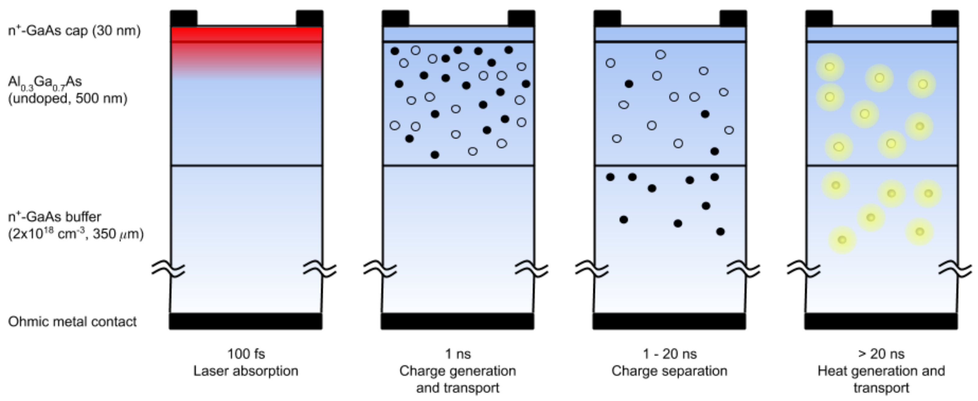
1. Introduction
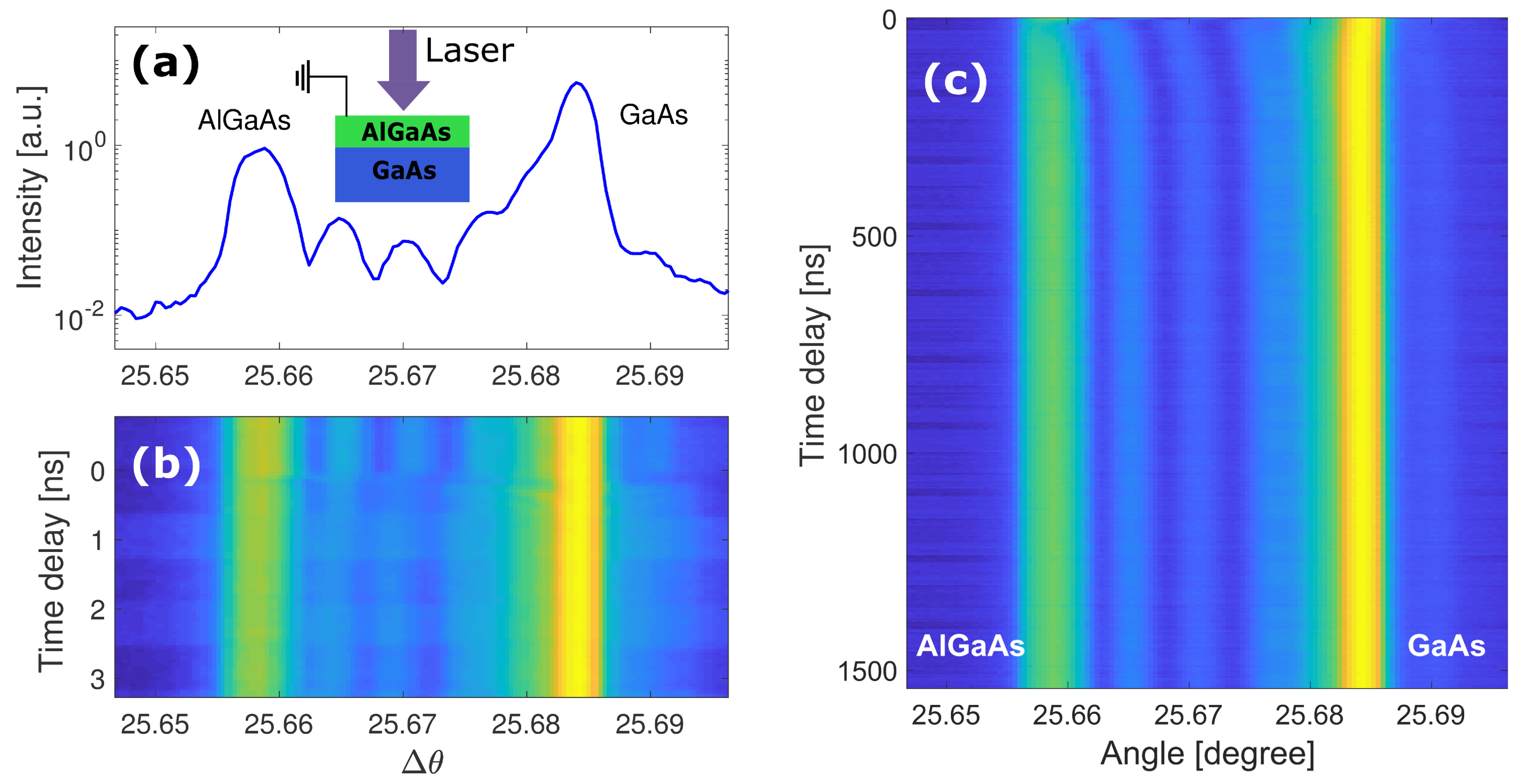
2. Materials and Methods
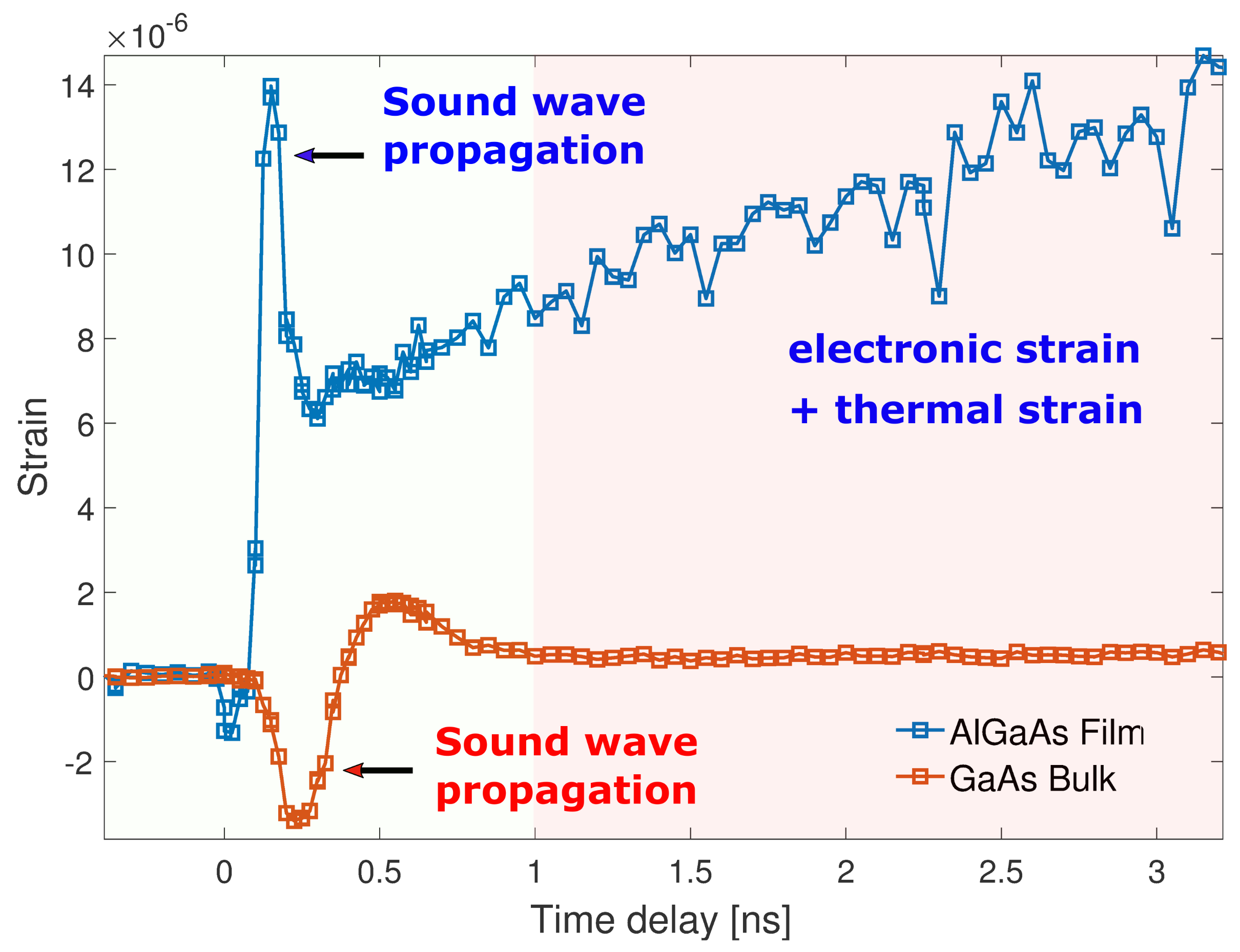
3. Results
4. Discussion
5. Conclusions
Author Contributions
Funding
Acknowledgments
Conflicts of Interest
References
- Bardeen, J.; Shockley, W. Deformation Potentials and Mobilities in Non-Polar Crystals. Phys. Rev. 1950, 80, 72–80. [Google Scholar] [CrossRef]
- Habermehl, C.L.; Newell, J.T. Electronic Pressure-Sensitive Semiconductor Device. U.S. Patent 3,470,392, 30 September 1969. [Google Scholar]
- Figielski, T. Photostriction effect in germanium. Physica Status Solidi (B) 1961, 1, 306–316. [Google Scholar] [CrossRef]
- Stearns, R.; Kino, G. Effect of electronic strain on photoacoustic generation in silicon. Appl. Phys. Lett. 1985, 47, 1048–1050. [Google Scholar] [CrossRef]
- Takata, K.; Nakasuji, S.; Nishino, T.; Osaka, R.; Matsushita, Y. Photo-induced strain imaging of semiconductors. AIP Adv. 2017, 7, 045104. [Google Scholar] [CrossRef]
- Wei, S.H.; Zunger, A. Predicted band-gap pressure coefficients of all diamond and zinc-blende semiconductors: Chemical trends. Phys. Rev. B 1999, 60, 5404. [Google Scholar] [CrossRef]
- Baumberg, J.; Williams, D.; Köhler, K. Ultrafast acoustic phonon ballistics in semiconductor heterostructures. Phys. Rev. Lett. 1997, 78, 3358. [Google Scholar] [CrossRef]
- Lindenberg, A.; Kang, I.; Johnson, S.L.; Missalla, T.; Heimann, P.; Chang, Z.; Larsson, J.; Bucksbaum, P.; Kapteyn, H.; Padmore, H.; et al. Time-resolved X-ray diffraction from coherent phonons during a laser-induced phase transition. Phys. Rev. Lett. 2000, 84, 111. [Google Scholar] [CrossRef] [PubMed]
- Lee, S.; Cavalieri, A.; Fritz, D.; Swan, M.; Hegde, R.; Reason, M.; Goldman, R.; Reis, D. Generation and propagation of a picosecond acoustic pulse at a buried interface: Time-resolved X-ray diffraction measurements. Phys. Rev. Lett. 2005, 95, 246104. [Google Scholar] [CrossRef] [PubMed]
- Williams, G.J.; Lee, S.; Walko, D.A.; Watson, M.A.; Jo, W.; Lee, D.R.; Landahl, E.C. Direct measurements of multi-photon induced nonlinear lattice dynamics in semiconductors via time-resolved X-ray scattering. Sci. Rep. 2016, 6, 39506. [Google Scholar] [CrossRef] [PubMed]
- Lee, S.; Williams, G.J.; Campana, M.I.; Walko, D.A.; Landahl, E.C. Picosecond X-ray strain rosette reveals direct laser excitation of coherent transverse acoustic phonons. Sci. Rep. 2016, 6, 19140. [Google Scholar] [CrossRef] [PubMed]
- Jo, W.; Landahl, E.C.; DiChiara, A.D.; Walko, D.A.; Lee, S. Measuring femtometer lattice displacements driven by free carrier diffusion in a polycrystalline semiconductor using time-resolved X-ray scattering. Appl. Phys. Lett. 2018, 113, 032107. [Google Scholar] [CrossRef]
- Pudell, J.; Maznev, A.A.; Herzog, M.; Kronseder, M.; Back, C.H.; Malinowski, G.; von Reppert, A.; Bargheer, M. Layer specific observation of slow thermal equilibration in ultrathin metallic nanostructures by femtosecond X-ray diffraction. Sci. Rep. 2018, 9, 3335. [Google Scholar] [CrossRef] [PubMed]
- Dufresne, E.M.; Adams, B.; Arms, D.A.; Chollet, M.; Landahl, E.C.; Li, Y.; Walko, D.A.; Wang, J. Time-Resolved Research at the Advanced Photon Source Beamline 7-ID. AIP Conf. Proc. 2010, 1234, 181–184. [Google Scholar]
- Williams, G.J.; Watson, M.A.; Arms, D.A.; Mooney, T.M.; Walko, D.A.; Landahl, E.C. EPICS oscilloscope for time-resolved data acquisition. Nucl. Instrum. Methods Phys. Res. Sect. A Accel. Spectrom. Detect. Assoc. Equip. 2011, 649, 84–86. [Google Scholar] [CrossRef]
- Thomsen, C.; Grahn, H.T.; Maris, H.J.; Tauc, J. Surface generation and detection of phonons by picosecond light pulses. Phys. Rev. B 1986, 34, 4129. [Google Scholar] [CrossRef] [PubMed]
- DeCamp, M.F.; Reis, D.A.; Cavalieri, A.; Bucksbaum, P.H.; Clarke, R.; Merlin, R.; Dufresne, E.; Arms, D.; Lindenberg, A.M.; MacPhee, A.; et al. Transient strain driven by a dense electron-hole plasma. Phys. Rev. Lett. 2003, 91, 165502. [Google Scholar] [CrossRef] [PubMed]
- Sheu, Y.; Lee, S.; Wahlstrand, J.; Walko, D.; Landahl, E.; Arms, D.; Reason, M.; Goldman, R.; Reis, D. Thermal transport in a semiconductor heterostructure measured by time-resolved X-ray diffraction. Phys. Rev. B 2008, 78, 045317. [Google Scholar] [CrossRef]
- Wie, C.; Tombrello, T.T.; Vreeland, T., Jr. Dynamical X-ray diffraction from nonuniform crystalline films: Application to X-ray rocking curve analysis. J. Appl. Phys. 1986, 59, 3743–3746. [Google Scholar] [CrossRef]
- Stepanov, S. Method of transfer matrices and dynamical thick-crystal approximation in surface X-ray diffraction by multilayer structures. Crystallogr. Rep. 1994, 39, 182–187. [Google Scholar]


© 2019 by the authors. Licensee MDPI, Basel, Switzerland. This article is an open access article distributed under the terms and conditions of the Creative Commons Attribution (CC BY) license (http://creativecommons.org/licenses/by/4.0/).
Share and Cite
Lee, S.; Jo, W.; DiChiara, A.D.; Holmes, T.P.; Santowski, S.; Cho, Y.C.; Landahl, E.C. Probing Electronic Strain Generation by Separated Electron-Hole Pairs Using Time-Resolved X-ray Scattering. Appl. Sci. 2019, 9, 4788. https://doi.org/10.3390/app9224788
Lee S, Jo W, DiChiara AD, Holmes TP, Santowski S, Cho YC, Landahl EC. Probing Electronic Strain Generation by Separated Electron-Hole Pairs Using Time-Resolved X-ray Scattering. Applied Sciences. 2019; 9(22):4788. https://doi.org/10.3390/app9224788
Chicago/Turabian StyleLee, Sooheyong, Wonhyuk Jo, Anthony D. DiChiara, Timothy P. Holmes, Stephen Santowski, Yong Chan Cho, and Eric C. Landahl. 2019. "Probing Electronic Strain Generation by Separated Electron-Hole Pairs Using Time-Resolved X-ray Scattering" Applied Sciences 9, no. 22: 4788. https://doi.org/10.3390/app9224788
APA StyleLee, S., Jo, W., DiChiara, A. D., Holmes, T. P., Santowski, S., Cho, Y. C., & Landahl, E. C. (2019). Probing Electronic Strain Generation by Separated Electron-Hole Pairs Using Time-Resolved X-ray Scattering. Applied Sciences, 9(22), 4788. https://doi.org/10.3390/app9224788