Article

Correlation between the Morphology of ZnO Layers and the Electroluminescence of Quantum Dot Light-Emitting Diodes

Department of Advanced Materials Engineering, Kyonggi University, Suwon 16227, Korea
*
Author to whom correspondence should be addressed.
Appl. Sci. 2019, 9(21), 4539; https://doi.org/10.3390/app9214539
Submission received: 19 September 2019 / Revised: 17 October 2019 / Accepted: 23 October 2019 / Published: 25 October 2019
(This article belongs to the Special Issue High Dielectric Constant Nanoparticles)

Abstract

:
The present work shows the effect of the ZnO layer morphology on inverted quantum dot light-emitting diodes (QLEDs) using different spin-coating processes. In the inverted structure of ITO/ZnO/QDs/CBP/MoO3/Al, ZnO nanoparticles were used as the electron transport layer. The utilization of a two-step spin-coating process to deposit a ZnO layer on a patterned ITO glass substrate resulted in an increase in the surface roughness of the ZnO layer and a decrease in the luminance of the QLEDs. However, the current efficiency of the device was enhanced by more than two-fold due to the reduced current density. Optimization of the ZnO spin-coating process can efficiently improve the optical and electrical properties of QLEDs.

1. Introduction

Colloidal quantum dots (QDs) have attracted widespread attention as promising materials due to their tunable emission wavelength, high color purity, and near-unity photoluminescence quantum yield. In particular, quantum dot light-emitting diodes (QLEDs) are expected to provide the excellent emission characteristics of QDs and the benefits of solution processing techniques [1,2,3,4]. Peng and coworkers demonstrated highly efficient QLEDs with an external quantum efficiency (EQE) of 20.5% based on the optimization of the charge balance [5]. As both the emission layer (EML) and the charge transport layer in QLEDs can be fabricated using a solution process, this approach is more economical than the standard high-vacuum deposition systems.
The most common solution process is the spin-coating technique. In the early stages of research on standard-structured QLEDs, both the hole transport layer (HTL) and EML were formed by the spin-coating process, and then the organic electron transport layer (ETL) was deposited by the thermal evaporation process [6,7]. Now, however, chemically stable ZnO nanoparticles (NPs) have replaced the organic molecules for the ETL and the resultant device performance has been outstanding [8,9,10]. Despite the necessity of the spin-coating process for all the layers of QLEDs, the majority of research has focused on analyzing and improving the inorganic material itself, and a comparative study has not been conducted on the one-step and two-step deposition of ZnO NPs in terms of device performance.
Herein, we report the significant changes in the luminance and efficiency of QLEDs according to the changed morphology. In the spin-coating process, the step schedule is set as a variable to analyze the generated morphology. Both the one-step- and two-step-coated QLEDs exhibit excellent optoelectronic performance, but the devices with the two-step deposition of the ZnO NPs show a current efficiency approximately 2.3 times higher than that with one-step deposition. The correlation between the surface morphology and device performance is analyzed through atomic force microscopy (AFM) images. The results indicate that, in addition to the material properties and the device structure, the surface morphology of each layer should also be considered for achieving highly efficient QLEDs.

2. Materials and Methods

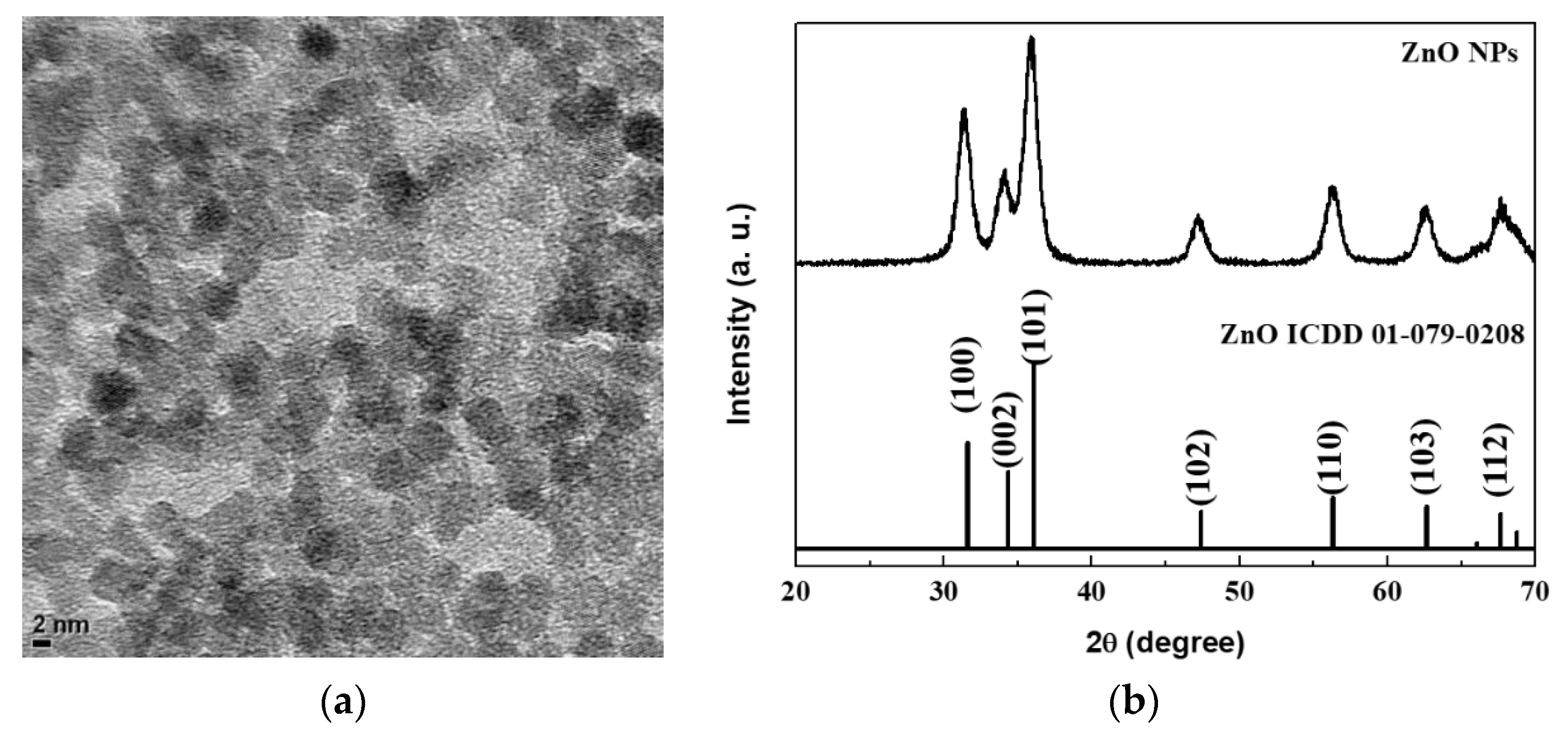
2.1. Synthesis of ZnO NPs

For a typical reaction of ZnO NPs, 5 mmol of Zn acetate dehydrate was dissolved in 30 mL of dimethyl sulfoxide. A mixture of 5 mmol of tetramethylammonium hydroxide in 10 mL of ethanol (99.9%, HPLC grade) was added dropwise to the above clear solution, and the reaction continued for 1 h at room temperature. Then, by introducing excess acetone, as-synthesized ZnO NPs were precipitated and finally redispersed in ethanol.

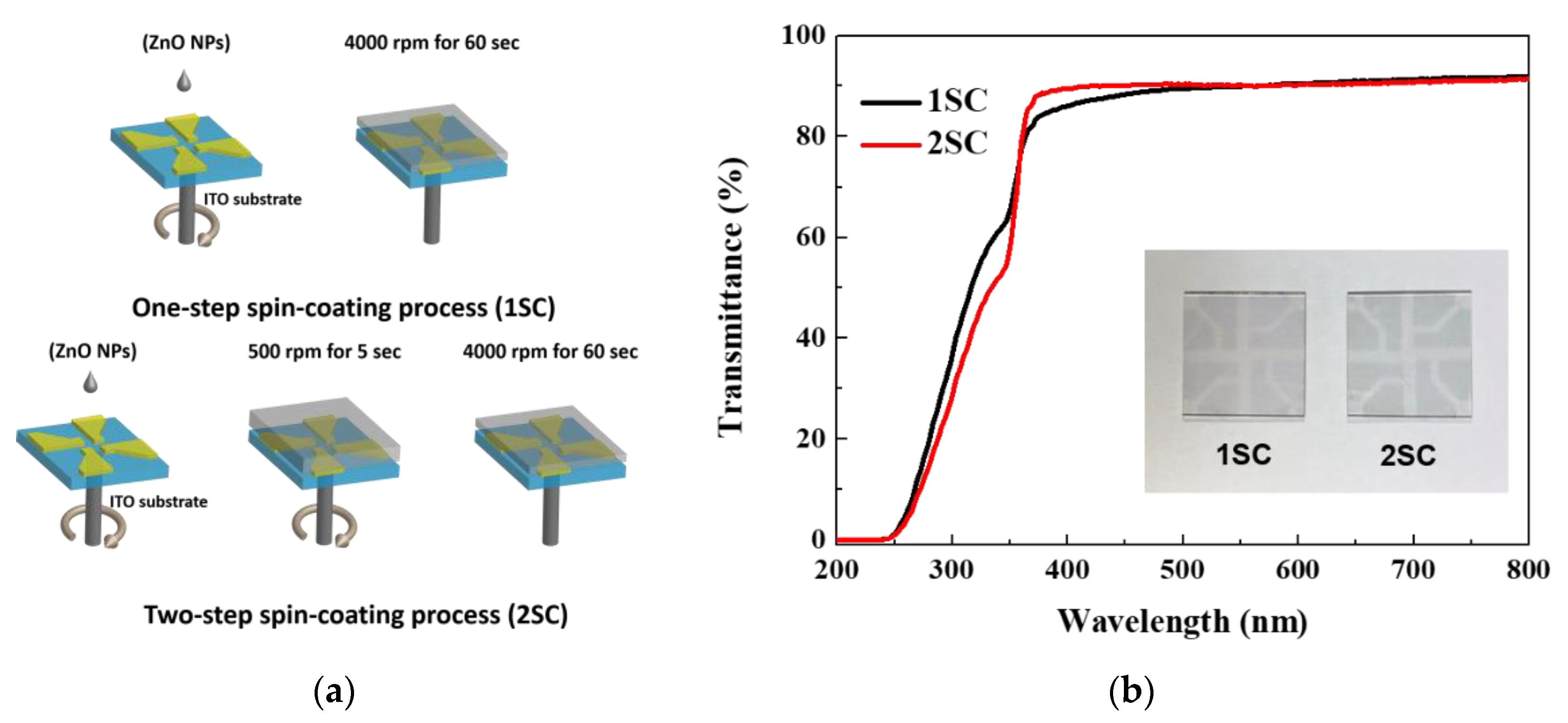
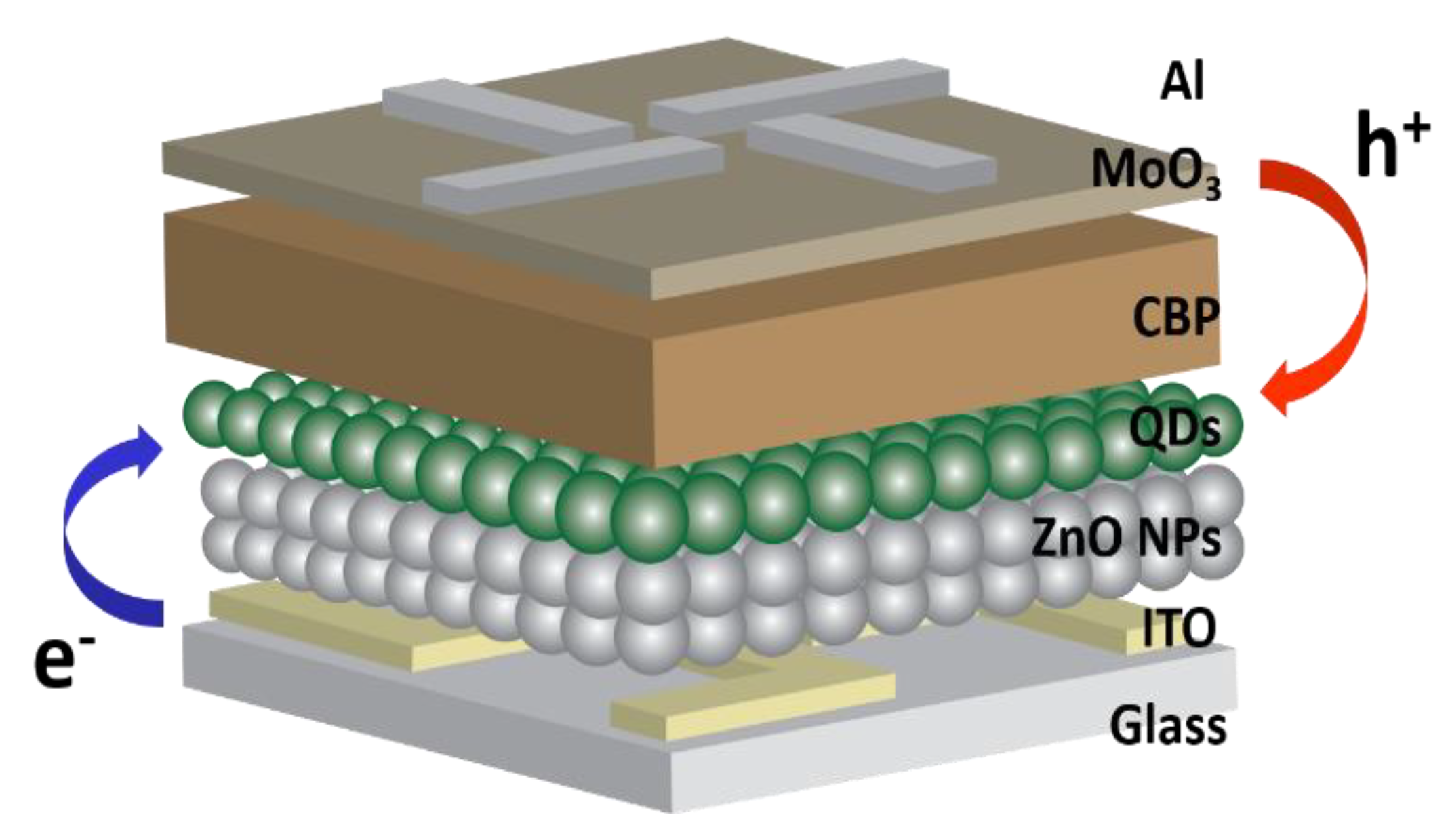
2.2. Fabrication of QLEDs

Indium-tin-oxide (ITO)-coated glass substrates were used for the fabrication of QLEDs. The substrates were sequentially cleaned with isopropyl alcohol and rinsed with deionized water. Then, the patterned ITO substrates underwent ultraviolet-ozone treatment for 15 min. ZnO NPs for the ETL were deposited on the treated ITO substrates by two-step spin-coating at a spin rate of 500 rpm for 5 s and 4000 rpm for 60 s. Next, CdZnSeS/ZnS QDs (In-visible Inc., Suwon, Korea) were spin-cast on top of the ITO/ZnO NPs substrates at a spin rate of 2000 rpm for 5 s. The size, peak wavelength, and linewidth of QDs were 12 nm, 529 nm, and 20 nm, respectively (Figure S1). The organic materials and metals were continuously deposited by thermal evaporation without breaking the vacuum condition. We thermally evaporated 4,4′-bis (carbazol-9-yl) biphenyl (CBP) (for the HTL), MoO3, and Al at a deposition rate of approximately 2 Å/s for CBP, approximately 0.5 Å/s for MoO3, and approximately 5 Å/s for the Al electrode. Finally, the device encapsulation process was carried out using encapsulation glass and ultraviolet (UV)-curable polymer resin.

2.3. Characterization
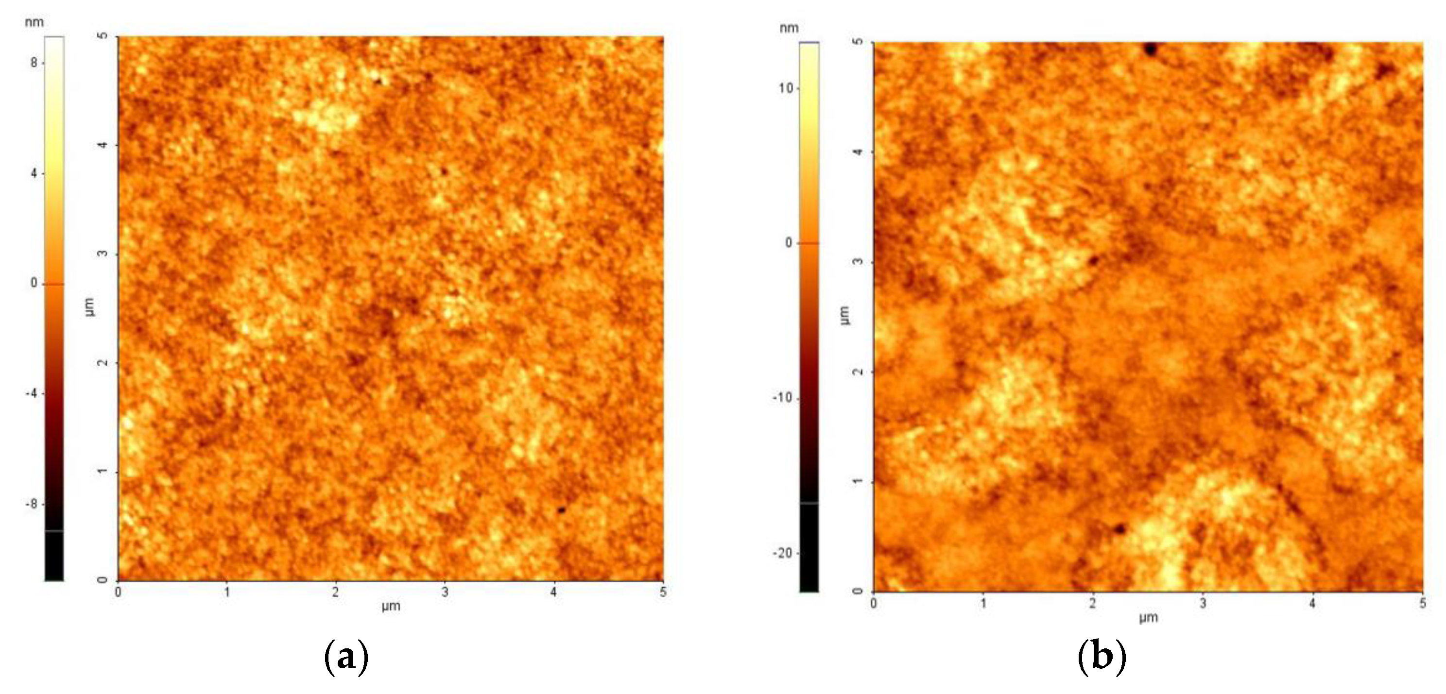
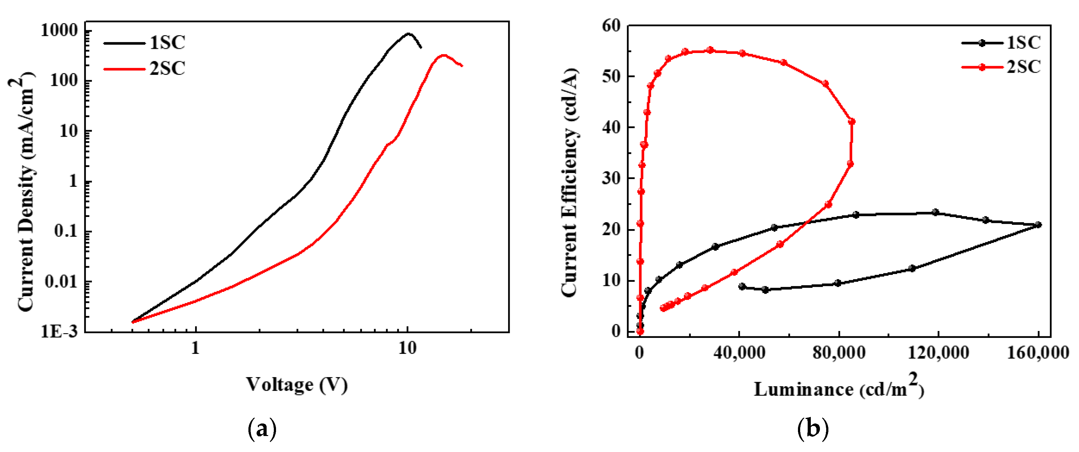
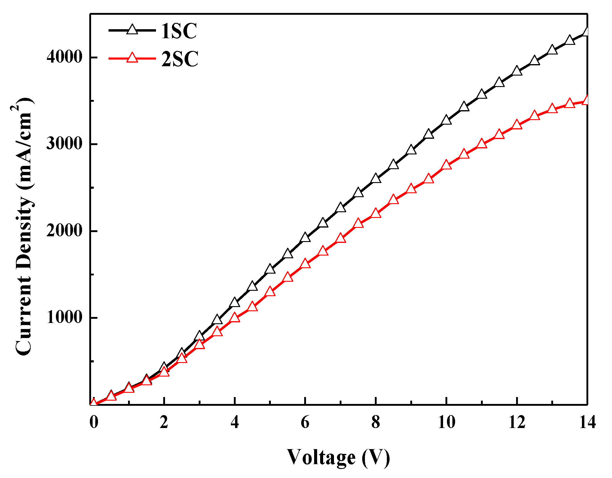
The electroluminescence (EL) spectra and current density–voltage–luminance (J–V–L) characteristics of the QLEDs were measured by using a spectroradiometer (Konica-Minolta CS-2000) with a source meter (Keithley 2400) under ambient conditions. The surface profiles of the ZnO NPs layer were measured by AFM (PSIA XE 100). The transmission electron microscopy (TEM) work was performed using a JEOL JEM-2100F to obtain images of the ZnO NPs. The X-ray diffraction (XRD) pattern of the synthesized ZnO NPs was obtained using a Rigaku MiniFlex II X-ray diffractometer.

3. Results

A TEM image of the synthesized ZnO NPs is shown in Figure 1a. The ZnO NPs are nearly spherical and have an average diameter of 4 nm. Figure 1b shows the XRD pattern of the ZnO NPs together with that of the bulk phase ZnO. A comparison of the diffraction peaks suggests that the ZnO NPs are crystalline and adopt the wurtzite structure of the bulk ZnO. The small particle size leads to a significant broadening of the characteristic diffraction peaks from the ZnO NPs.
Figure 2a shows an illustration of two different spin-coating processes for the ETL using ZnO NPs. Generally, the ETL is formed by a one-step spin-coating process (1SC, 4000 rpm for 60 s). However, in this study, one more step at a faster speed was added before the maximum rpm. Thus, the devices were fabricated with a two-step spin-coating process (2SC, 500 rpm for 5 s → 4000 rpm for 60 s). The transmittance spectra for the ZnO layers with different step schedules are shown in Figure 2b. The transmittance of both ZnO layers is more than 80% [11] and there is no significant difference between the layers throughout the entire visible region.
Figure 3 shows the AFM images of the ZnO layer on patterned ITO glass with different step schedules of the spin-coating process. The morphology of the ZnO layer was investigated to determine its effect on the optical and electrical performance of the QLEDs. The surface roughness of the ZnO layer using the 2SC was increased due to the addition of a second step.
Figure 4 presents a schematic device structure of the inverted QLEDs, which consist of ITO (cathode)/ZnO NPs (70 nm)/green QDs (12 nm)/CBP (40 nm)/MoO3 (10 nm)/Al (anode) [12]. There was no significant difference in the thickness of both ZnO layers with 1SC and 2SC (Figure S2). In contrast to the standard QLEDs, electrons are injected from the ITO, then transported to the QDs (EML) through the ZnO NPs (ETL) and holes are injected from the Al, then transported to the QDs (EML) through the MoO3 and CBP (HTL). Due to the low conduction band and valence band edge (−4.3 and −7.6 eV, respectively) of ZnO, the electrons move easily from the ITO to the EML while the holes are blocked at the interface between the EML and the ETL [3]. This is a huge advantage for highly efficient QLEDs because a higher rate of radiative recombination can occur in the EML.
Figure 5a represents the voltage-dependent variations of the current density of QLEDs with different step schedules of the spin-coating process. The current density is significantly reduced by the additional step of the spin-coating process. At a voltage of 5 V, which is close to the turn-on voltage, the current density of the device with 1SC is 19.71 mA/cm2, while that with 2SC is only 0.27 mA/cm2. Figure 5b shows the current efficiency as a function of the luminance of QLEDs with different step schedules. Interestingly, the devices with 1SC are brighter and less efficient than those with 2SC (maximum luminance: 160,030 vs. 85,083 cd/m2 and current efficiency: 23.33 vs. 55.23 cd/A, respectively). This is because the difference in the current density is much greater than the difference in the luminance. In detail, the maximum luminance of the devices with 1SC is approximately twice as bright but the current density is also more than ten times higher compared to the devices with 2SC.
Figure 6 presents the current density–voltage characteristics of electron-only devices (EODs). The current density of EODs with 2SC was also reduced like whole devices. Since the thickness difference of ZnO layers by two processes is less than 10% (Figure S2), the roughness of the ZnO layer is considered as the major factor affecting the current density in the QLEDs [13]. The low current density of the devices with 2SC is attributed to the increased roughness (from 1.398 to 2.645 nm) of the ZnO layer caused by the additional spin step, as shown in Figure 3. Finally, highly efficient QLEDs with a current efficiency of 55.23 cd/A were achieved with 2SC of the ZnO layer while maintaining a brightness of 85,083 cd/m2.
In a mobile display, the current efficiency is more important than the luminance due to the limited battery power. In this work, we found that the optical and electrical properties of the QLEDs were affected by the morphology of the ZnO layer, which is directly related to the spin-coating process.

4. Conclusions

The inverted-structured QLEDs were fabricated using two different spin schedules for the ZnO layer to evaluate the correlation between the morphology of the ZnO layer and the optical/electrical properties of the devices. Two ZnO layers showed no significant difference in the transmittance spectra in the visible region, but the current density of the devices with two-step spin-coating was decreased due to the rough surface caused by the additional step. The luminance of the devices with two-step spin-coating was lower than those with one-step spin-coating, but the current efficiency was significantly improved from 23.33 to 55.23 cd/A due to the decrease in the current density. The results on the optimization of the spin-coating process for the ZnO layer demonstrated the efficiently improved performance of the inverted QLEDs.

Supplementary Materials

The following are available online at https://www.mdpi.com/2076-3417/9/21/4539/s1, Figure S1: (a) PL and absorption spectra and (b) TEM image of CdZnSeS/ZnS QDs, Figure S2: Cross-sectional SEM images of ZnO layer on patterned ITO glass with (a) 1SC and (b) 2SC.

Author Contributions

Investigation, S.O. and J.K.; writing—original draft preparation, S.O.; writing—review and editing, J.K.; funding acquisition, J.K.

Funding

This work was supported by World Class 300 Project R&D grant (No. S2434857) by Korea Small and Medium Business Administration and the National Research Foundation of Korea (NRF) grant funded by the Korea government (MSIT) (No. 2017R1A2B4012274). This work was also supported by Kyonggi University’s Graduate Assistantship 2019.

Conflicts of Interest

The authors declare no conflict of interest.

References

  1. Colvin, V.L.; Schlamp, M.C.; Alivisatos, A.P. Light-emitting diodes made from cadmium selenide nanocrystals and a semiconducting polymer. Nature 1994, 370, 354–357. [Google Scholar] [CrossRef]
  2. Mashford, B.S.; Stevenson, M.; Popovic, Z.; Hamilton, C.; Zhou, Z.; Breen, C.; Steckel, J.; Bulovic, V.; Bawendi, M.; Coe-Sullivan, S.; et al. High-efficiency quantum-dot light-emitting devices with enhanced charge injection. Nat. Photonics 2013, 7, 407–412. [Google Scholar] [CrossRef]
  3. Lee, K.H.; Lee, J.H.; Song, W.S.; Ko, H.; Lee, C.; Lee, J.H.; Yang, H. Highly efficient, color-pure, color-stable blue quantum dot light-emitting devices. ACS Nano 2013, 7, 7295–7302. [Google Scholar] [CrossRef] [PubMed]
  4. Han, C.-Y.; Yang, H. Development of colloidal quantum dots for electrically driven light-emitting devices. J. Korean Ceram. Soc. 2017, 54, 449–469. [Google Scholar] [CrossRef]
  5. Dai, X.; Zhang, Z.; Jin, Y.; Niu, Y.; Cao, H.; Liang, X.; Chen, L.; Wang, J.; Peng, X. Solution-processed, high-performance light-emitting diodes based on quantum dots. Nature 2014, 515, 96–99. [Google Scholar] [CrossRef] [PubMed]
  6. Coe, S.; Woo, W.K.; Bawendi, M.; Bulović, V. Electroluminescence from single monolayers of nanocrystals in molecular organic devices. Nature 2002, 420, 800–803. [Google Scholar] [CrossRef] [PubMed]
  7. Bae, W.K.; Kwak, J.; Park, J.W.; Char, K.; Lee, C.; Lee, S. Highly efficient green-light-emitting diodes based on CdSe@ZnS quantum dots with a chemical-composition gradient. Adv. Mater. 2009, 21, 1690–1694. [Google Scholar] [CrossRef]
  8. Stouwdam, J.W.; Janssen, R.A.J. Red, green, and blue quantum dot LEDs with solution processable ZnO nanocrystal electron injection layers. J. Mater. Chem. 2008, 18, 1889–1894. [Google Scholar] [CrossRef]
  9. Qian, L.; Zheng, Y.; Xue, J.; Holloway, P.H. Stable and efficient quantum-dot light-emitting diodes based on solution-processed multilayer structures. Nat. Photonics 2011, 5, 543–548. [Google Scholar] [CrossRef]
  10. Kim, J.H.; Han, C.Y.; Lee, K.H.; An, K.S.; Song, W.; Kim, J.; Oh, M.S.; Do, Y.R.; Yang, H. Performance improvement of quantum dot-light-emitting diodes enabled by an alloyed ZnMgO nanoparticle electron transport layer. Chem. Mater. 2015, 27, 197–204. [Google Scholar] [CrossRef]
  11. Lin, Z.; Chang, J.; Jiang, C.; Zhang, J.; Wu, J.; Zhu, C. Enhanced inverted organic solar cell performance by post-treatments of solution-processed ZnO buffer layers. RSC Adv. 2014, 4, 6646–6651. [Google Scholar] [CrossRef]
  12. Oh, S.; Han, C.Y.; Yang, H.; Kim, J. Highly efficient white electroluminescent devices with hybrid double emitting layers of quantum dots and phosphorescent molecules. Nanoscale 2019, 11, 9276–9280. [Google Scholar] [CrossRef] [PubMed]
  13. Kim, H.M.; Youn, J.H.; Seo, G.J.; Jang, J. Inverted quantum-dot light-emitting diodes with solution-processed aluminium-zinc oxide as a cathode buffer. J. Mater. Chem. C 2013, 1, 1567–1573. [Google Scholar] [CrossRef]
Figure 1. (a) transmission electron microscopy (TEM) image and (b) X-ray diffraction (XRD) pattern of ZnO nanoparticles (NPs).
Applsci 09 04539 g001
Figure 2. (a) Schematic description of two different spin-coating processes for the electron transport layer (ETL) using ZnO NPs and (b) transmittance spectra of ZnO layers on patterned ITO glass substrate.
Applsci 09 04539 g002
Figure 3. Atomic force microscopy (AFM) images of ZnO layer on patterned ITO glass with (a) one-step spin-coating process (1SC, roughness root mean square (Rrms) = 1.398 nm) and (b) two-step spin-coating process (2SC, Rrms = 2.645 nm).
Applsci 09 04539 g003
Figure 4. Device structure of the inverted quantum dots light-emitting diodes (QLEDs).
Applsci 09 04539 g004
Figure 5. (a) Current density–voltage and (b) current efficiency–luminance characteristics of QLEDs with 1SC and 2SC of the ZnO layer.
Applsci 09 04539 g005
Figure 6. Current density–voltage characteristics of electron-only devices (EODs) with 1SC and 2SC of the ZnO layer.
Applsci 09 04539 g006

