Article

Effect of ElectroSpark Process Parameters on the WE43 Magnesium Alloy Deposition Quality

1
Dipartimento di Meccanica, Matematica e Management (DMMM), Politecnico di Bari, Viale Japigia, 182, 70126 Bari, Italy
2
Innovation Engineering Department, University of Salento, Via per Arnesano s,n, 73100 Lecce, Italy
*
Author to whom correspondence should be addressed.
Appl. Sci. 2019, 9(20), 4383; https://doi.org/10.3390/app9204383
Submission received: 31 July 2019 / Revised: 28 September 2019 / Accepted: 12 October 2019 / Published: 17 October 2019
(This article belongs to the Special Issue Microstructural and Mechanical Properties of Metallic Materials)

Abstract

:
This research aims to investigate the effects of process parameters on the quality of WE43 coatings deposited on homologue substrate by ElectroSpark Deposition (ESD) technology. ESD is new technology used to apply coatings or for the restoration and refurbishment of worn or damaged high valued parts. The depositions were processed using five different levels of Energy input (Es, Spark Energy). The microstructure of both the base material and deposits cross-section were characterized by optical and scanning electron microscopies. Also, X-ray diffraction technique was used. In addition, stereological studies of the through-thickness heterogeneities of the deposits (e.g., voids) were performed. The mechanical properties were evaluated by Vickers micro-hardness. The results show that the deposits exhibited a fine grained microstructure due to the rapid solidification. The average micro-hardness values of the deposits are lower than that of the substrate and distributed in a small range (49–60 HV). The lower hardness of the deposits respect to the base material is due to the presence of defectiveness such as spherical, laminar and random shaped voids. The defects area percentage inside the deposits remains well below than 11%. All the deposits were mainly affected by laminar morphology defects. The results indicate that the deposits defectiveness decreases as the energy input increases.

Graphical Abstract

1. Introduction

Over the last few decades, aerospace and aeronautical industries have shown a strong interest for the coating/repair procedures of high-valued parts through the use of safe, reliable, economic and environmentally friendly innovative technologies [1,2]. The majority of the conventional deposition processes (such as HVOF, PVD, CVD, electro plating and etc.,) used to improve components’ wear and corrosion resistance are characterized by high costs equipment, length processing, and pollution [3,4,5]. Furthermore, these techniques are not suitable to coat or repair the heat sensitive alloys widely used in aerospace applications (i.e., aluminum and magnesium alloy) due to the high thermal input involved that induces a large heat affected zone (HAZ), residual stresses and distortions [1,4,5,6,7,8,9]. These effects deserve attention because typically they degrade the mechanical performances.
The aeronautical industries commonly employ light materials such as aluminum and magnesium alloys for producing components [10]. Particularly, the WE43 alloy, belonging to the magnesium-rare earth-zirconium (Mg–RE–Zr) system, is the most used between existing magnesium alloys because of its high specific strength, good castability and machinability, high thermal conductivity, high dimensional stability, good electromagnetic shielding property together with improved mechanical properties up to 250 °C. At the same time, this alloy is characterized by low creep resistance and poor stability of the properties when exposed at temperatures above 300 °C. The WE43 alloy is often used for helicopter transmissions, power systems, aero engines, gearbox casings, missiles, and sport cars engine blocks [11,12,13,14]. That alloy is usually processed by casting and exhibits various defects like shrinkage porosity and cracks [11,12,13,14]. Due to the cracks susceptibility of WE43 alloy, the conventional high heat input deposition techniques are not suitable for the repair of the WE43 components [15,16,17].
In this context, ElectroSpark Deposition (ESD) technology appears as a very interesting solution to apply coatings to improve corrosion and wear-resistance and for the restoration of damaged high valued parts particularly for those materials ordinarily considered un-weldable by conventional weld processes [2,18,19,20,21]. In fact, ESD is a type of low heat-input pulsed micro-bonding process where a consumable material electrode is deposited onto a conductive component’s surface through a series of high-energy density electrical pulses of short duration, typically ranging from a few microseconds to milliseconds. In the ESD process, the electric arc generated between the electrode tip and the substrate is able to melt a small material volume fraction of both the substrate and the electrode. Specifically, the small molten droplets from the electrode are propelled and accelerated by the electric field towards the substrate where they crash. The single drop of electrode material that impinges on the substrate is identified with the term “splat”, while the resulting morphology of the deposit surface is therefore defined as “a splash”. During the advancement of the electrode, the drops are deposited in sequence on the substrate generating thin layers of material. In ESD process the bonds between the adjacent splats or splat/substrate develop by both melting and diffusion [22,23,24,25,26].
The many benefits of ESD include a low-pollution, the technological simplicity of metal deposition at atmospheric pressure, the portability of the equipment for use in shop or in field and the low cost of the machine. Moreover, being a low heat input process, usually ESD does not induce distorsions or microstructural changes in heat sensitive substrate and is applicable to those materials possessing a high tendency to cracks during welding such as superalloys, MCrAlY and thermally sensitive materials [24,25,26,27,28].
According to the set of process parameters the microstructure of the deposits has been observed both amorphous or extremely fine grained [22,23]. For example, Cadney and Brochu [29] show the feasibility of using the ESD process to deposit amorphous electrode material (Zr41.2Ti13.8Ni10Cu12.5Be22.5) onto an amorphous substrate of the same composition without crystallizing the deposit or the substrate. Hasanabadi et al. [30] investigated the ESD coating structure of as-cast Fe48Cr18Mo7B16C4Nb7 crystalline alloy on 316L stainless steel substrate. In particularly, their results showed that the coating structure is amorphous at low total heat input values, but at high values of total heat input, an extremely fine-grained or likely nano-crystalline structure was obtained.
Some studies have analyzed both microstructure and defects of 2024 aluminum alloy coatings deposited onto a homologue substrate by ESD process [19,31]. Moreover, the effect of the ESD process as a repair technology was studied by P. Leo et al [32] and P. D. Enrique et al. [33] respectively for a 2024 aluminum alloy and Ni-Superalloy. Especially, regarding the aluminum alloy, a comparative study between deposits performed on substrates supplied both in natural aged and artificial aged state has been performed. Results showed that the as-repaired samples had low tensile properties due to defectiveness and residual stress. However, it has been demonstrated that the tensile performances can be improved by post repair heat-treatments.
Others researchers studied in detail the mass transfer mechanism in the ESD process. In particular, Gallinov and Luban have developed a method to determine the efficiency of mass transfer, also called transfer coefficient, constantly monitoring the erosion of the anode and the mass gain of the cathode [34].
Until now, the opportunity of applying the ESD technology to WE43 magnesium alloy has not been studied, despite the huge interest in many sectors, first of all the aeronautic one.
This work is the first study regarding the application of ESD process on WE43 magnesium alloy. Especially, the ESD technique was used to deposit WE43 coatings on homologue substrate. Five depositions at increasing levels of spark energy were processed. The discussion will involve the effect of the spark energies on the microstructural and mechanical features for the production of high performance and reliable deposits. Additionally, since during the WE43 alloy deposition process different defects could occur, the relationship between the processing energies and the area fraction and morphology of these defects was investigated. The identification and examination of these defects is a very important topic since their presence may exert significant influence on the deposits’ mechanical properties.

2. Experimental Details

2.1. Materials and Processing

In this study, WE43 magnesium alloy electrodes were used for coating homologue substrate. The chemical composition (wt %) of the WE43 alloy is shown in Table 1. The WE43 magnesium alloy substrate was supplied in artificially aged condition as 15 mm thick discs. Bars of 80 × 20 mm were cut from those discs. The artificial peak-aging heat treatment involved solubilization at 525 °C – 8 h, quenching in hot water at 60 °C and aging in a hot oil bath at 250 °C for 16 h followed by air cooling. The consumable electrode was a cylindrical rod with a diameter of 2.3 mm and length about of 50 mm.
The depositions were performed at room temperature using a “Technocoat MicroDepo Model 150” machine. Before starting the depositions, each substrate was polished with 800-grit SiC paper in order to remove the oxide films and any surface defects. The WE43 deposits were processed using a hand-held gun and performing multiple–layer depositions always on a same line as shown in Figure 1. After setting the energy value, each layer was deposited by multiple depositions along the substrate surface in OY direction with a constant deposition travel speed. In particular, for each value of the spark energy, 50 subsequent deposition layers were performed following the OZ direction (Figure 1).
During depositions the electrode rotation speed and discharge frequency (f) were kept constant at 1200 rpm and 390 Hz, respectively. In addition, all the depositions were performed in the presence of a constant Argon flow equal to 10 L/min. The two main electrical parameters, voltage and capacitance, were properly varied in order to change the energy input. The spark pulse-energy in joule (J) of each set of parameters given in the Table 2 was determined as follows:
E s = 1 2 C V 2
where C is the capacitance in Farad (F) and V is the voltage in Volt (V) [31].
Especially in this study, the effect of five spark pulse-energy values ranging from 0.15 and 1.69 J (Table 2) on the quality of the coatings has been analyzed.

2.2. Metallographic Characterization and Stereological Studies

After the deposition, the coatings were cross sectioned using a diamond blade. After the cut, the depositions cross sections were cold mounted in epoxy resin, grinded and mechanically polished. The microstructure analysis was performed after Picral’s etching (100 mL ethanol and 4 g picric acid). While, the stereological study of the through-thickness defectiveness of the deposits were performed in the as-polished condition. The examinations were performed by conventional analytical techniques such as Optical Microscope (OM) Nikon Epiphot 200 supplied by a computer-assisted image analysis (NIS Elements AR) and Scanning Electron Microscope (SEM) Zeiss EVO equipped with energy dispersive spectrometry (EDS) technique using a Brucker electron microprobe. Moreover, a Rigaku X-ray diffractometer (XRD) in Cu Kα radiation was used to study the phase composition of the base material, the electrode and the metal deposited layers. Especially, diffraction patterns were obtained from 15° to 85° with step size of 0.02° and a dwell time of 2 sec; for 40 KV voltage and an operating current of 20 mA.
The through-thickness defectiveness of the deposits was analyzed using ImageJ software. In particular, within the deposits cross-section the defects size and morphology (voids) were estimated. The size has been identified by the perimeter, area and Feret diameter while the defects morphology by shape factor (fcircle), defined as:
f c i r c l e = 4 π A P 2
where P is the perimeter and A is the area of defect. Thus, for a perfect circle (spherical defect), the shape factor (fcircle) value would be equal to one, while for strongly elongated defects and therefore laminar the fcircle value would be very close to zero.
The identified defects were distinguished in the following three classes:
  • laminar shaped defects or cracks (0 < fcircle < 0.4),
  • random shaped defects (0.4 < fcircle < 0.7)
  • spherical shaped defects (0.7 < fcircle < 1).
Additionally, the thickness of each deposit was assessed by carrying out an average of five measurements respectively at a half of the substrate/deposit interface length and ±250 µm and ±500 µm from the same.

2.3. Mechanical Properties Measurement: Vickers Micro-Hardness

Micro-hardness test, carried out in accordance with ASTM E-384, was performed with the use of WIKI 200 JS type micro-hardness tester. A load of 300 g for 15 s was used for the indentations. Ten measurements were carried out on both electrode and substrate in order to calculate the average micro-hardness values.
On the deposit cross section, the micro-hardness measurements were performed following a line arrangement parallel substrate/deposit interface. The measurements were realized at 100 µm from each other and from the interface. Also another indentations line parallel and at 100 µm from the interface was performed on the substrate in order to characterize the effect of heat input on the base material microstructure. Subsequently, the average values of microhardness were calculated considering all the indentation made in the deposit zone and in the interface, respectively.

3. Results and Discussion

3.1. Microstructure of WE43 Base Material

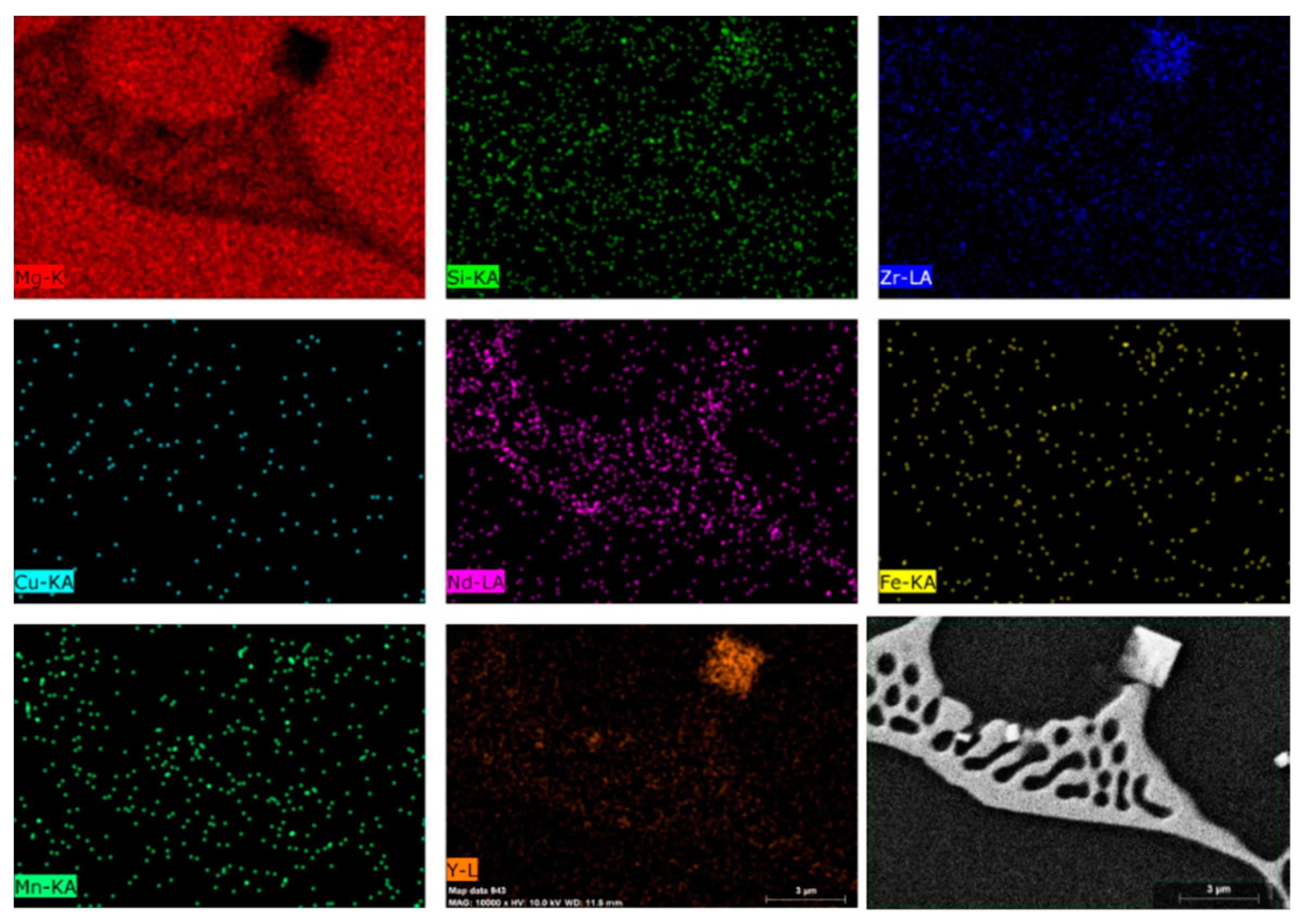
OM and SEM micrographs of the base material in transverse section (XZ plane) are shown in Figure 2. The alloy microstructure consisting of α-Mg grains (Figure 2a), amounts of intermetallic eutectic phase which mainly aggregate at the grain boundaries (Figure 2a–c) and some precipitates of cuboid-shaped distributed within the matrix and around the eutectic (see the arrow in Figure 2b). The SEM–EDS map scan (Figure 3) reveals that the eutectic phase contains mainly Nd while the elements Y and Zr are more concentrated in cuboid-shaped phase. Indeed, Nd is concentrated in the intermetallic eutectic phase due to the low solubility in the Mg matrix [35], on the contrary Zr is distributed also in the Mg matrix. The XRD measurements indicate (Figure 4) that the substrate is mainly composed of five phases: α-Mg (Card N°35-0821), Mg24Y5 (Card N°31-0817), Mg41Nd5 (Card N°45-1031), MgY and β (Mg14Nd2Y) phase. In the electrode microstructure three main compounds were identified: α-Mg (Card N°35-0821), Mg24Y5 (Card N°31-0817), Mg12Nd (Card N°17-0401). In the XRD patterns, the Zr-rich phase has not been detected due to low volume fraction [36].
The micro-hardness (HV0.3/15) of the electrode and substrate alloy was 78 ± 1 and 75 ± 4 HV, respectively.

3.2. Microstructure of the Deposits

The solidification microstructure (parallel to the build direction) in the central region of the WE43 deposit without chemical-etching it is shown in Figure 5. The microstructure of the deposits, regardless of the process parameters, was characterized by a fine grained microstructure throughout the whole deposit.
The fine grained microstructure can be attributed to the high cooling rates that the melted splat undergoes in contact with the cold substrate (rapid solidification process). Generally, during the ESD process the cooling rates may reach 105–106 °C/s [22,23]. Furthermore, the bond interfaces with the previously deposited material are not observed, unlike what was found for deposits via ESD in light alloy [19,31,32].
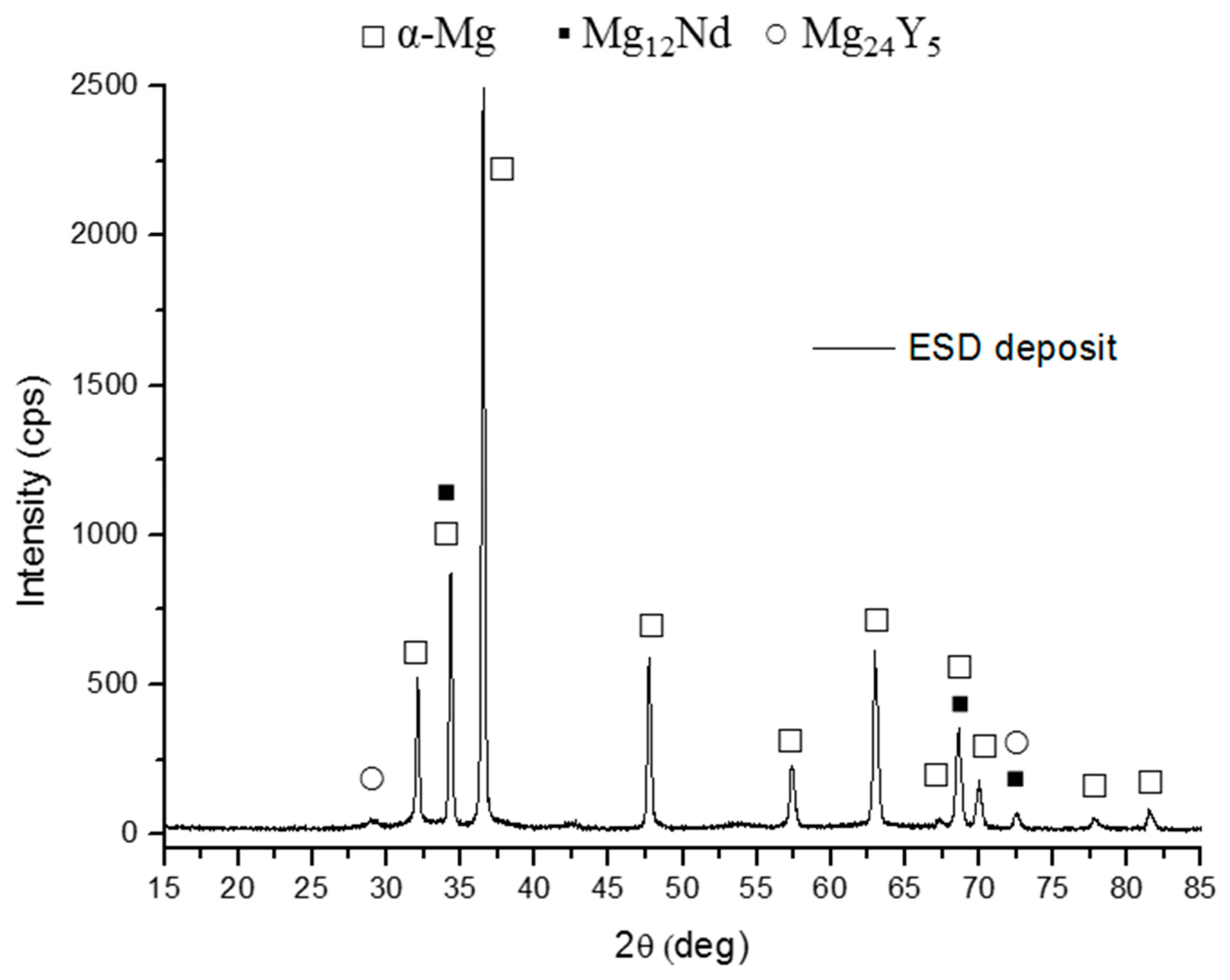
The deposit microstructure consists of semi-continuous Mg24Y5 and Mg12Nd phase distributed throughout an Mg matrix (as indicated by the XRD results, Figure 6). The XRD peaks present within the ESD deposited material representing both the α-Mg (Card N°35-0821), Mg24Y5 (Card N°31-0817) and Mg12Nd (Card N°17-0401) phase displayed significant rise with respect to the electrode pattern indicating gain of these phases during deposition (compares Figure 4 and Figure 6, respectively).
Figure 7 shows the microstructure close to the substrate/deposit interfacial region in WE43 deposit. The finer microstructure of the coating can be observed in Figure 7a,b. The mixing between the base material and the coating microstructure is shown in Figure 7b,c. Particularly eutectic structures embedded in the deposit close to the interface (Figure 7b) exhibits only some small dissolution (Figure 7b,c).

3.3. Analysis of Defects of WE43 Deposits

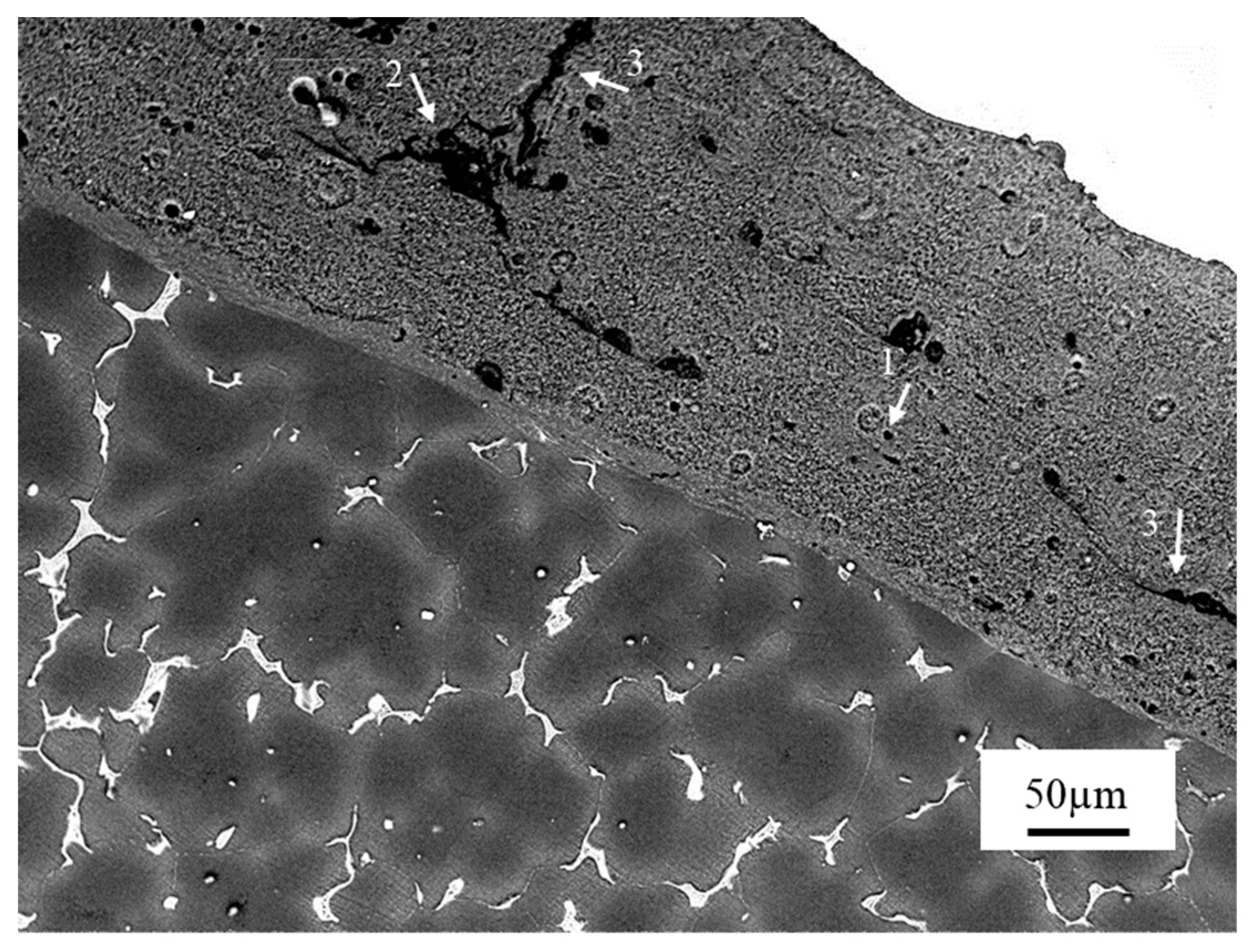
The built-up deposits, unfortunately, are affected by defects (Figure 8). The main defects detected in the deposits occur as voids of different morphology: spherical or random shaped defects (n°1 e n°2, respectively) and laminar defects (n° 3) that extend both perpendicularly and parallel to the substrate/deposit interface. The spherical or random shaped defects are believed to be the result of the amount of material brought to melting and its distribution [25,31,32,37]. While generally, the formation of laminar shaped defects was considered as a normal consequence of thermal stress induced by the high thermal gradients inherent to the ESD process. Especially, the perpendicular cracks to the interface are due to shrinkage during cooling and solidification of the deposited material. The perpendicularly cracks can arise in the first deposited layers, in the subsequent ones or nucleate on random shaped defects inside the deposits [38]. Usually, during the deposition process these cracks propagate upwards owing to repeated thermal stress [31,32]. Instead, the parallel cracks to the interface, also known as delamination cracks, can be generated by poor mixing of the electrode material with the substrate or layer previously deposited (weakly bounded interfaces) or by the mechanical impact of the electrode tip to the workpiece [31,39].
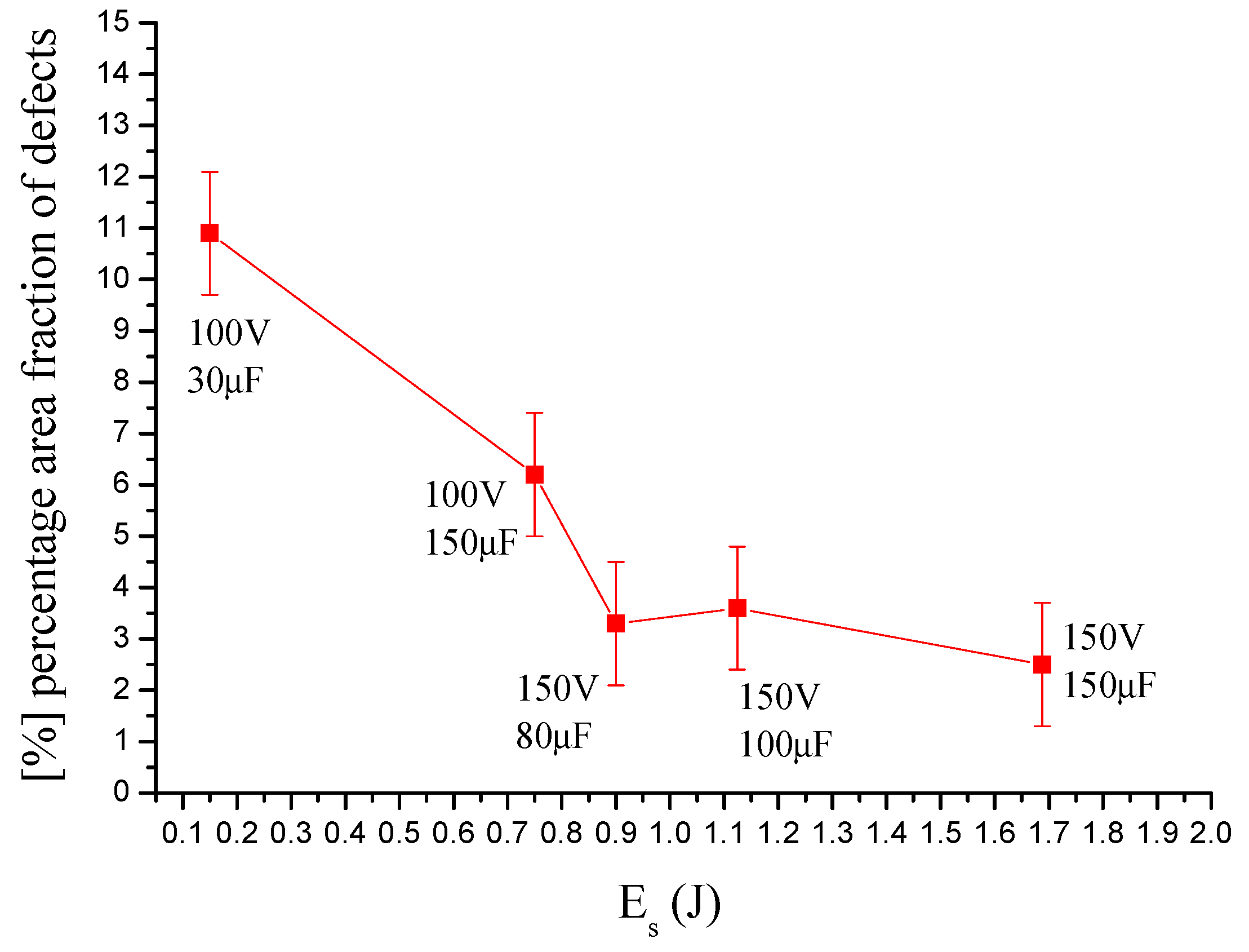
Figure 9 presents the percentage area fraction of defects, calculated as the ratio between the area of voids and the area of the deposit, as a function of pulse energy (Es). The plot (Figure 9) illustrates that the increase of Es reduces the percentage area fraction of defects. At low energy values (s1 and s2) the deposits display a greater percentage area fraction of defects, while at higher Es values (s3–s5) the percentage area fraction of each deposits is smaller and does not significantly change with Es. It can also be observed that the percentage area fraction of defects remains small for all the samples and is well below 11%. The defects diameters dispersion is a function of the shape factor for the lowest (s1), highest (s5), and intermediate (s3) value of deposition energy is shown in Figure 10. As shown, the laminar and spherical defects are characterized, respectively, by the maximum and by minimum extension. Moreover, the size of the spherical defects is contained and less than 30 µm, while the size of the random and laminar defects exhibits a greater variability.
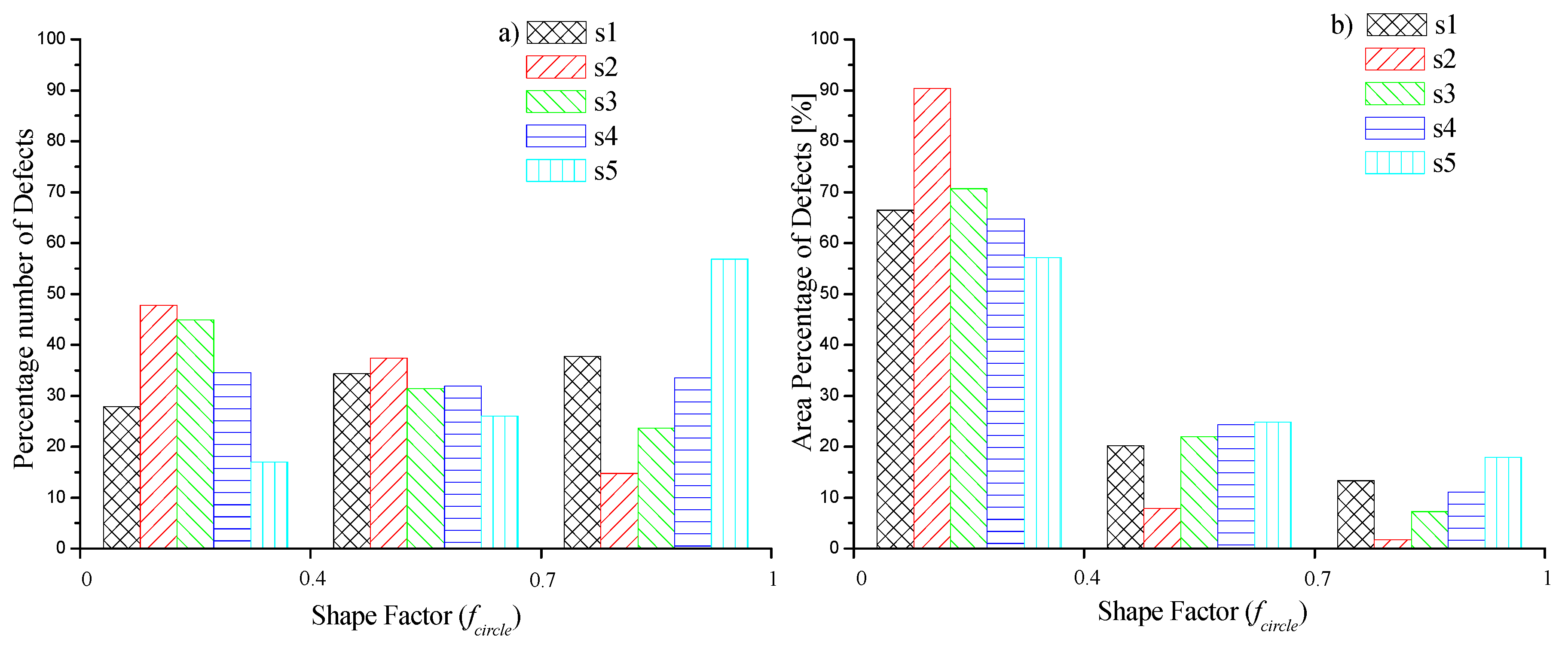
A better understanding of deposits defectiveness, as a function of process parameters can be obtained by calculating the percentage number of defects and area defects for classes of shape factor. Therefore, Figure 11a,b represent the percentage number of defects and defects area percentage for each class of the shape factor (laminar, random and spherical), respectively. Percentage number is defined as the ratio between the defects number for each class and the total defects number in the deposit, while the defects area percentage is defined as the ratio between defects area for each class of shape factor and the total area of the deposit.
Results (Figure 11a) showed that for Es value higher than 0.75 J, the defects percentage number decreases for the laminar shaped defects (0 < fcircle < 0.4) and increases for the spherical shaped defects (0.7 < fcircle < 1). No significant differences were observed between the percentage number of random shaped defects (0.4 < fcircle < 0.7) as Es increases. The defects area percentage (Figure 11b) shows similar trends to the percentage number as a function of Es. It can also be observed that all the deposits were mainly occupied by laminar shaped defects while the spherical shaped defects only occupy the lowest area percentage (Figure 11b). Therefore, as Es increases both the number and area of laminar/spherical defects decreases/increases.
With higher Es, the amount of molten material of the electrode the re-melting of the substrate material increase. This leads to a better mixing of the film of molten material both of the electrode and substrate contributing to the reduction of the laminar defects. Moreover, both the lower cooling rate induced by the increased amount of melted materials and the higher average temperature of the previous deposited layer, due to the higher heat input reduce the nucleation of cracks [30,38]. The spherical defects were associated to the generation and subsequent closure of surface asperities or roughness [29] favored by higher voltages and capacitance values [27,40]. The roughness is mainly due to the fragmentation of the molten droplets after their impact against the substrate (splashing) and their subsequent rapid solidification. The extent of this roughness increases with increasing Es because the amount of splashed molten material. Consequently, the non-uniform distribution of molten droplets generates asperities and increases the spherical defects. Additionally, these spherical shaped defects may be attributed also to gas porosity. Therefore, we observed an overall increase in the number of spherical defects with increasing Es and, consequently, an increase in the percentage area.

3.4. Effect of the Electric Parameters on Mechanical Properties and Thickness of Deposits

The mechanical properties of the deposits as a function of process parameters were investigated by indentations of micro-hardness (HV0.3/15) on polished cross-sections of the deposits. Average micro-hardness value of deposits are shown in Table 3, as well as the average micro-hardness value of measurements performed in the substrate close to the interface. The results show that the sample processed at the lowest Es (s1) exhibits the lowest hardness value, while no significant difference exists between the average hardness values of deposits processed at Es higher of 0.75 J. In addition, even if the deposits microstructure was finer grained respect to the substrate (see Figure 5), it can be noticed that all deposits present an average micro-hardness value lower than that of the substrate (75 ± 4 HV), regardless of the processing parameters. The lower hardness of the deposits respect to the base material can be attributed to the presence of widespread defectiveness within them. Indeed the deposits performed using low Es (0.15 and 0.75 J) exhibited higher percentage area fraction of defects than those performed with Es of 0.9, 1.125 and 1.69 J. These last ones displays both constant and slightly higher micro-hardness value (Table 3) due to the lower percentage area fraction value. In the substrate micro-hardness values at 100 µm far from the interface (Table 3) does not vary respect to the base material, confirming (as shown in Figure 7) that the low thermal contribution of the process does not change significantly the microstructure and mechanical properties of the substrate.
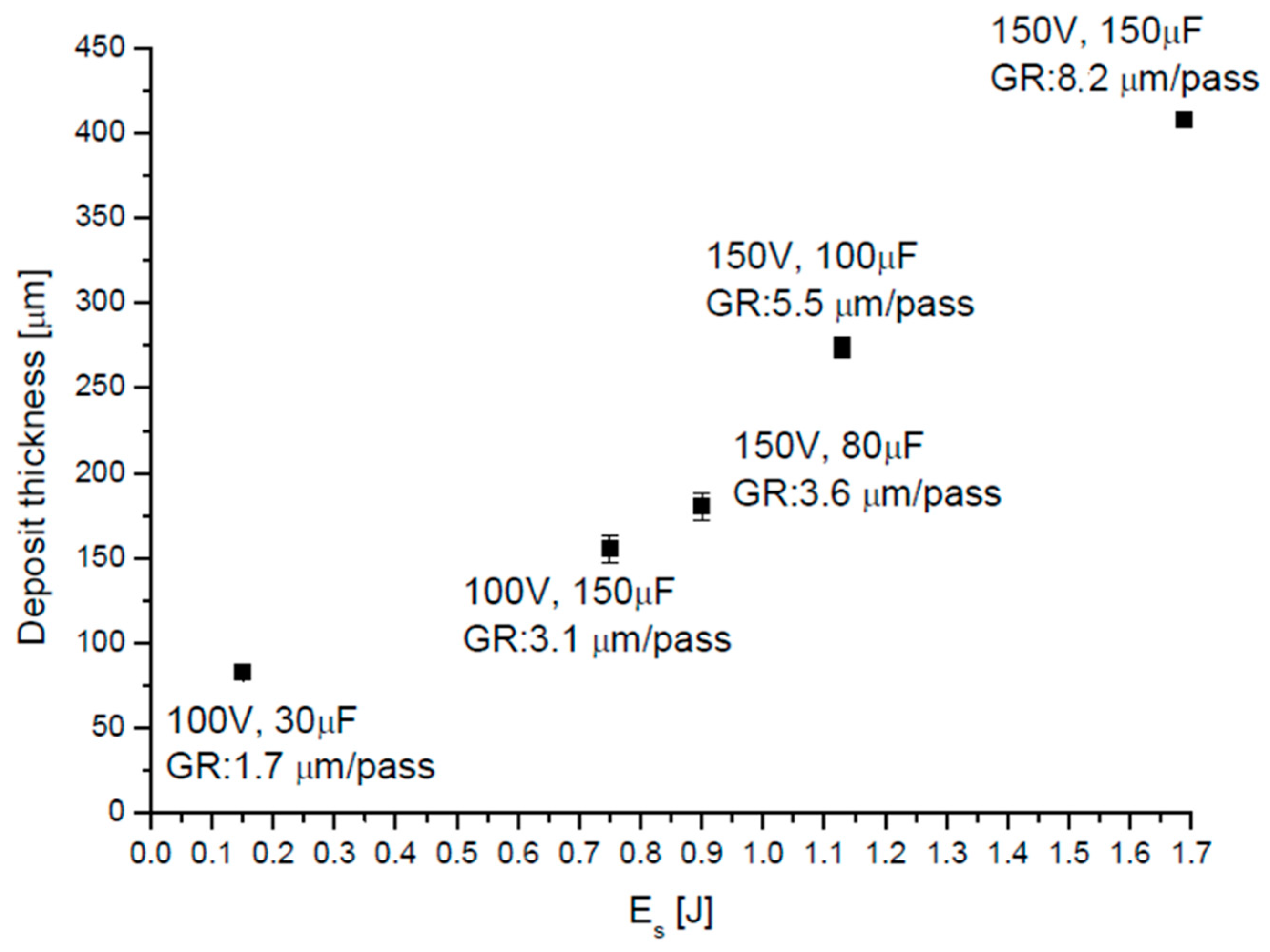
The results presented in Figure 12 demonstrate that the WE43 deposits thickness is related to the pulse-spark energy. Indeed, the thickness increases with deposition pulse energy, ranging from 82.6 μm for the deposit produced at the lowest energy to 407.6 μm for the deposit produced at the highest Es. This is due to the increased amount of material being transferred at higher spark energy (Es) [41], that rises the deposit growth rate (GR). Therefore, for a given number of deposited layers, the increasing of Es, lead also to a reduced deposition time.

4. Conclusions

This paper was devoted to study the effects of the Energy Input values on the deposition quality of WE43 magnesium alloy on homologue substrate by ElectroSpark technology. Based on the analysis of the results, the following conclusions can be drawn:
  • The deposits’ microstructure was very fine grained due to the rapid solidification process. The XRD patterns of the coating and starting material are similar.
  • The coatings’ thickness increases significantly with the spark pulse-energy.
  • In the coating/substrate interface of WE43 alloy deposit a partial dissolution of the eutectic structures has been observed. In addition, the substrate micro hardness close to the coating interface does not change with process parameters, indicating that the heat input of the process does not alter significantly the substrate microstructure.
  • The deposits cross-section exhibit several discontinuities that occur as voids. With increasing of the heat input the percentage of defectiveness was reduced. Particularly with increasing of the spark energy the laminar shape defects are reduced.
  • The average micro-hardness values of the deposits are lower than that of the substrate and ddistributed in a small range (49–60 HV). The coatings micro-hardness values reflect the trend of the defectiveness.

Author Contributions

Conceptualization, G.R. and P.L.; Methodology, G.R. and P.L.; Investigation, G.R.; Data curation, G.R.; Writing—original draft preparation, G.R. and P.L.; Writing—review and editing, G.R. and P.L.; Visualization, G.R., P.L. and C.C.; Supervision C.C.

Funding

This research received no external funding.

Conflicts of Interest

The authors declare that they have no conflicts of interest.

References

  1. Paydas, H.; Mertens, A.; Carrus, R.; Lecomte-Beckers, J.; Tchuindjang, T. Laser cladding as repair technology for Ti–6Al–4V alloy: Influence of building strategy on microstructure and hardness. Mater. Des. 2015, 85, 497–510. [Google Scholar] [CrossRef]
  2. Felix, L.M.; Kwan, C.C.; Zhou, N.Y. The Effect of Pulse Energy on the Defects and Microstructure of Electro-Spark-Deposited Inconel 718. Metall. Mater. Trans. A 2019, 50, 4223–4231. [Google Scholar] [CrossRef]
  3. Cao, T.; Lei, S.; Zhang, M. The friction and wear behavior of Cu/Cu-MoS2 self-lubricating coating prepared by electrospark deposition. Surf. Coat. Technol. 2015, 270, 24–32. [Google Scholar] [CrossRef]
  4. Feldshteina, E.E.; Kardapolova, M.K.; Gaida, R.; Khorodyski, B.; Kaval’chuk, O.V. Tribological Properties of ElectrosparkDeposited and Further Laser Hardened Coatings. J. Frict. Wear 2013, 34, 137–141. [Google Scholar] [CrossRef]
  5. Renna, G.; Leo, P.; Cerri, E.; Zanon, G.P. Thermal shock behaviour of CoCrAlTaY coatings on a Ni-base superalloy. Metall. Ital. 2015, 107, 33–41. [Google Scholar]
  6. Brandt, M. Laser Additive Manufacturing: Materials, Design, Technologies, and Applications; Woodhead Publishing: Cambridge, UK, 2016. [Google Scholar]
  7. Barile, C.; Casavola, C.; Pappalettera, G.; Pappalettere, C. Analysis of crack propagation in stainless steel by comparing acoustic emissions and infrared thermography data. Eng. Fail. Anal. 2015, 69, 35–42. [Google Scholar] [CrossRef]
  8. Mao, Y.; Li, Z.; Feng, K.; Guo, X.; Zhou, Z.; Wu, Y. Corrosion behavior of carbon film coated magnesium alloy with electroless plating nickel interlayer. J. Mater. Process. Technol. 2015, 219, 42–47. [Google Scholar] [CrossRef]
  9. Ermakova, E.N.; Sysoev, S.V.; Nikulina, L.D.; Tsyrendorzhieva, I.P.; Rakhlin, V.I.; Kosinova, M.L. Synthesis and characterization of organosilicon compounds as novel precursors for CVD processes. Thermochim. Acta 2015, 622, 2–8. [Google Scholar] [CrossRef]
  10. Campbell, F.C. Manufacturing Technology for Aerospace Structural Materials; Elsevier: Amsterdam, Netherlands, 2006. [Google Scholar]
  11. Turowska, A.; Adamiec, J. Mechanical properties of WE43 magnesium alloy joint at elevated temperature. Arch. Metall. Mater. 2015, 60, 2695–2701. [Google Scholar] [CrossRef]
  12. Kierzek, A.; Adamiec, J. Creep Resistance of WE43 Magnesium Alloy Joints Solid State Phenomena. Trans. Tech. Publ. 2012, 191, 177–182. [Google Scholar]
  13. Gupta, M.; Wong, W.L.E. Magnesium–based nanocomposites lightweight materials of the future. Mater. Charact. 2015, 105, 30–46. [Google Scholar] [CrossRef]
  14. Rashad, M.; Pan, F.; Lin, D.; Asif, M. High temperature mechanical behavior of AZ61 magnesium alloy reinforced with graphene nanoplatelets. Mater. Des. 2016, 89, 1242–1250. [Google Scholar] [CrossRef]
  15. Liu, J.; Yu, H.; Chen, C.; Weng, F.; Dai, J. Research and development status of laser cladding on magnesium alloys: A review. Opt. Lasers Eng. 2017, 93, 195–210. [Google Scholar] [CrossRef]
  16. McClelland, Z.; Avery, D.Z.; Williams, M.B.; Mason, C.J.T.; Rivera, O.G.; Leah, C.; Allison, P.G.; Jordon, J.B.; Martens, R.L.; Hardwick, N. Microstructure and Mechanical Properties of High Shear Material Deposition of Rare Earth Magnesium Alloys WE43. In Magnesium Technology; Springer: Switzerland, Germany, 2019; pp. 277–282. [Google Scholar]
  17. Kocurek, R.; Adamiec, J. The Repair Welding Technology of Casts Magnesium Alloy QE2. Solid State Phenom. 2014, 212, 81–86. [Google Scholar] [CrossRef]
  18. Carofalo, A.; Dattoma, V.; Nobile, R.; Panella, F.W.; Alfeo, G.; Scialpi, A.; Zanon, G.P. Mechanical Characterization of a Nickel-based Superalloy Repaired using MicroPlasma and ESD Technology. Procedia Eng. 2015, 109, 312–319. [Google Scholar] [CrossRef] [Green Version]
  19. Leo, P.; Renna, G.; Perulli, P.; Zanon, G.P.; Alfeo, G. Caratterizzazione microstrutturale e meccanica di rivestimenti in lega AA2024 ottenuti mediante electrospark deposition. In Proceedings of the 36° Conferenza Nazionale AIM, Parma, Italy, 21–23 September 2016. [Google Scholar]
  20. Cerri, E.; Renna, G.; Leo, P.; Zanon, G.P.; Alfeo, G. caratterizzazione di deposizioni di leghe leggere mediante electro spark deposition. In Proceedings of the 35° Conferenza Nazionale AIM, Bologna, Italy, 21–22 November 2014. [Google Scholar]
  21. Xiang, H.O.N.G.; Ke, F.E.N.G.; Tan, Y.F.; Wang, X.L.; Hua, T.A.N. Effects of process parameters on microstructure and wear resistance of TiN coatings deposited on TC11 titanium alloy by electrospark deposition. Trans. Nonferrous Met. Soc. China 2017, 27, 1767–1776. [Google Scholar]
  22. Frangini, S.; Masci, A. A study on the effect of a dynamic contact force control for improving electrospark coating properties. Surf. Coat. Technol. 2010, 204, 2613–2623. [Google Scholar] [CrossRef]
  23. Padgurskas, J.; Kreivaitis, R.; Rukuiža, R.; Mihailov, V.; Agafii, V.; Kriukiene, R.; Baltušnikas, A. Tribological properties of coatings obtained by electro-spark alloying C45 steel surfaces. Surf. Coat. Technol. 2017, 311, 90–97. [Google Scholar] [CrossRef]
  24. Xie, Y.J.; Wang, M.C. Microstructural morphology of electrospark deposition layer of a high gamma prime superalloy. Surf. Coat. Technol. 2006, 201, 691–698. [Google Scholar] [CrossRef]
  25. Champagne, V.; Pepi, M.; Edwards, B. Electrospark Deposition for the Repair of Army Main Battle Tank Components; Army Research Laboratory: Adelphi, MD, USA, 2006. [Google Scholar]
  26. Wang, W.F.; Wang, M.C.; Sun, F.J.; Zheng, Y.G.; Jiao, J.M. Microstructure and cavitation erosion characteristics of Al–Si alloy coating prepared by electrospark deposition. Surf. Coat. Technol. 2008, 202, 5116–5121. [Google Scholar] [CrossRef]
  27. Anisimov, E.; Khan, A.K.; Ojo, O.A. Analysis of Microstructure in Electro-Spark Deposited IN718 Superalloy. Mater. Charact. 2016, 119, 233–240. [Google Scholar] [CrossRef]
  28. Enrique, P.D.; Jiao, Z.; Zhou, N.Y. Effect of Direct Aging on Heat-Affected Zone and Tensile Properties of Electrospark-Deposited Alloy 718. Met. Mater. Trans. A 2019, 50, 285–294. [Google Scholar] [CrossRef]
  29. Cadney, S.; Brochu, M. Formation of amorphous Zr41.2Ti13.8Ni10Cu12.5Be22.5 coatings via the ElectroSpark Deposition process. Intermetallics 2008, 16, 518–523. [Google Scholar] [CrossRef]
  30. Hasanabadi, M.F.; Ghaini, F.M.; Ebrahimnia, M.; Shahverdi, H.R. Production of amorphous and nanocrystalline iron based coatings by electro-spark deposition process. Surf. Coat. Technol. 2015, 270, 95–101. [Google Scholar] [CrossRef]
  31. Leo, P.; Renna, G.; Casalino, G. Study of the Direct Metal Deposition of AA2024 by ElectroSpark for Coating and Reparation Scopes. Appl. Sci. 2017, 7, 945. [Google Scholar] [CrossRef]
  32. Renna, G.; Leo, P.; Casalino, G.; Cerri, E. Repairing 2024 Aluminum Alloy via Electrospark Deposition Process: A Feasibility Study. Adv. Mater. Sci. Eng. 2018, 1–11. [Google Scholar] [CrossRef]
  33. Enrique, P.D.; Jiao, Z.; Zhou, N.Y.; Toyserkan, E. Effect of microstructure on tensile properties of electrospark deposition repaired Ni-superalloy. Mater. Sci. Eng. A 2018, 729, 268–275. [Google Scholar] [CrossRef]
  34. Brochu, M.; Heard, D.W.; Milligan, J.; Cadney, S. Bulk nanostructure and amorphous metallic components using the electrospark welding process. Assem. Autom. 2010, 30, 248–256. [Google Scholar] [CrossRef]
  35. Avedesian, M.M.; Baker, H. Magnesium and Magnesium Alloys; ASM Handbook: Cleveland, OH, USA, 1999. [Google Scholar]
  36. Ascencio, M.; Pekguleryuz, M.; Omanovic, S. An investigation of the corrosion mechanisms of WE43 Mg alloy in a modified simulated body fluid solution: The influence of immersion time. Corros. Sci. 2014, 87, 489–503. [Google Scholar] [CrossRef]
  37. Verbitchi, V.; Ciuca, C.; Cojocaru, R. Electro-Spark Coating with Special Materials. Nonconv. Technol. Rev. 2011, 1, 57–62. [Google Scholar]
  38. Staia, M.H.; Fragiel, A.; Cruz, M.; Carrasquero, E.; Campillo, B.; Perez, R.; Constantino, M.; Sudarshan, T.S. Characterization and wear behavior of pulsed electrode surfacing coatings. Wear 2001, 251, 1051–1060. [Google Scholar] [CrossRef]
  39. Chen, Z.; Zhou, Y.H. Surface modification of resistance welding electrode by electro-spark deposited composite coatings: Part I. Coating characterization Surf. Coat. Technol. 2006, 201, 1503–1510. [Google Scholar] [CrossRef]
  40. Reynold, J.L.; Holdren, R.L.; Brown, L.E. Electro-Spark Deposition. Adv. Mater. Processes 2003, 161, 35–37. [Google Scholar]
  41. Heard, D.W.; Brochu, M. Development of a nanostructure microstructure in the Al–Ni system using the electrospark deposition process. J. Mater. Process. Technol. 2010, 210, 892–898. [Google Scholar] [CrossRef]
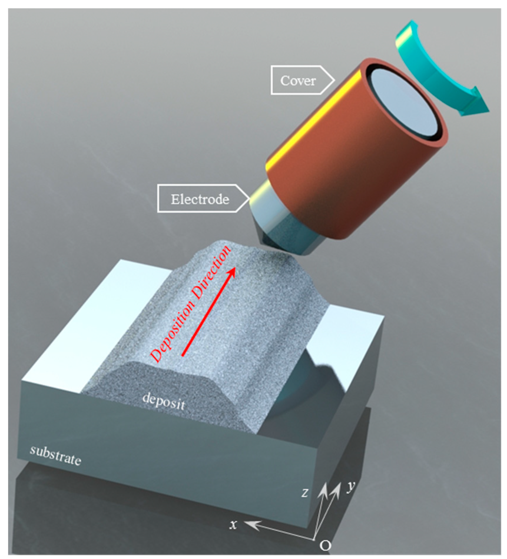
Figure 1. Representation of the ESD process.
Applsci 09 04383 g001
Figure 2. Microstructure of WE43: (a) Optical Microscope (OM) of the base material unattached showing the α-Mg grain structure and grain boundary eutectic structures, (b) backscattered electron (BSE) image illustrating the cuboidal intermetallic particles (precipitates) and the grain boundary eutectic structures (c) BSE image enlarged of the eutectic structure.
Applsci 09 04383 g002
Figure 3. Energy dispersive spectrometry (EDS) map scan of WE43 base material image showing the distribution of elements in alloy.
Applsci 09 04383 g003
Figure 4. X-ray diffractometer (XRD) patterns of the as-cast (electrode) and peak-aged WE43 alloy (base material).
Applsci 09 04383 g004
Figure 5. Microstructure parallel to the build direction (cross-section) in the central region of WE43 deposit: (a) OM and (b) SEM micrographs.
Applsci 09 04383 g005
Figure 6. XRD pattern of WE43 magnesium alloy deposit.
Applsci 09 04383 g006
Figure 7. Microstructure near the interface between the substrate and deposit: (a) OM and (b) SEM micrographs of WE43 deposit, (c) magnification of interface (as marked “B” in Figure 7b).
Applsci 09 04383 g007
Figure 8. SEM micrograph showing the typical voids of the ESD coating: small spherical voids (n°1), large, random shaped voids (n°2) and laminar porosity (n°3).
Applsci 09 04383 g008
Figure 9. Percentage area fraction of defects as a function of spark energy (Es) for WE43 deposits.
Applsci 09 04383 g009
Figure 10. Defects diameter distribution as a function of shape factor for: (a) the lowest (s1), (b) the intermediate (s3) and (c) the highest value of deposition energy (s5).
Applsci 09 04383 g010
Figure 11. Analysis of the defects in the deposits cross-section. (a) percentage number of defects and (b) percentage area of defects vs the three classes of shape factor (fcircle): (0–0.4) laminar defects, (0.4–0.7) spherical defects and (0.7–1) random shaped defects.
Applsci 09 04383 g011
Figure 12. Energy density (Es) vs. thickness for ESD deposits.
Applsci 09 04383 g012
Table 1. Chemical composition (wt %) of WE43 magnesium alloy.
ZnFeSiCuMnYNdZrMgOther
WE430.2030.00710.0050.009< 0.00013.9632.3880.409Bal.< 0.2
Table 2. Parameters of ESD process settings.
SampleVoltage [V]Capacitance [µF]Es [J]
s1100300.15
s21001500.75
s3150800.9
s41501001.13
s51501501.69
Table 3. Average hardness value (HV300/15) of deposit and of substrate at 100 µm far from the interface substrate/deposit.
Samples1s2s3s4s5
HV of deposits49 ± 3.558 ± 560.1 ± 4.660 ± 559.5 ± 3.2
HV at 100 µm far from the interface75 ± 273.5 ± 173 ± 172 ± 3 74.3 ± 1