1. Introduction
The well-known increase in information rate is a particular concern for inter-data center communication due to chromatic dispersion (CD). Increasing the rate of information reduces the optimal reachable transmission [
1]. Using an O-band for standard single-mode fibers, where the CD can almost be neglected, is one way to avoid needing to mitigate it. Nonetheless, transmission in the O-band has high attenuation, which reduces the length of the transmission link [
2]. Alternatively, solutions in the C-band, which address the intersymbol interference induced by dispersion, can also be considered [
3,
4,
5].
Coherent and direct detection (DD) systems are both possible technologies for C-band short-reach communication [
3,
6]. A coherent receiver has access to the amplitude and phase of the signal. Adding it together with digital signal processing (DSP), it brings with it huge potential to mitigate transmission impairments. However, inter-data center applications require cheaper and low-power transponders, which can be a challenge in these systems.
DD-receivers are the current alternative, but CD cannot be fully compensated in the digital domain as only the power is detected in the receiver. Different options for inter- and intra-data center interconnection, as well as for mobile fronthaul application for operation on the C-band have already been discussed in recent years [
4,
5]. A few of them operate on PAM-4 modulation and different options for DSP-based receiver equalization, such as Volterra and maximum likelihood sequence estimation (MLSE) [
7,
8,
9] and DSP-based pre-distortion, such as Tomlinson Harashima precoding and the kramers-kronig receiver [
10,
11]. Works with an on-off keying (OOK) modulation format have also been presented in the literature [
12]. Recently, further signal processing technologies for this application range have been proposed, such as DSP-implemented neural networks [
13,
14] or silicon photonic-based opto-electronic reservoir computers with analog electronic processing [
15].
Alternatively, optical dispersion compensation modules as fiber Bragg grating and dispersion compensation fibers are more commonly used to compensate for the CD in the optical domain. However, they are not easy to tune and need to be designed for a specific link. The latter also has issues with high attenuation and a large footprint.
Here, we propose a tuneable optoelectronic solution to mitigate the CD in DD systems. The processing structure we are investigating is located close to the approach using a simplified optical reservoir processor, discussed in [
15], together with an NN digital processor [
14]. This work is an extension of our preliminary results of [
16]. Here, we improve the digital equalization by using a neural network equalizer and propose a simplification of the optical structure to reduce footprint. The optical module slices the signal into narrow frequency sub-bands and delays them accordingly to the CD, before recombining everything back into a single signal. Increasing the number of sub-bands improves performance, but increases complexity. Alternatively, we show that the performance can be improved using the optical component with fewer sub-bands if a further stage of equalization in the digital domain is also applied. Furthermore, a complexity reduction is demonstrated by using half of the proposed optical module structure together with an NN equalizer. This approach slightly reduces the gain, but can be attractive for inter-data center communication due to the reduced footprint. Finally, the number of neurons required for the NN equalizer is analyzed.
The paper is organized as follows.
Section 2 presents the system description for short-reach communication and simulation setup.
Section 2.1 and
Section 2.2 describe the hybrid signal process module. The former is the optical structure used to mitigate CD, and the latter describes the NN equalization and training process.
Section 3 shows the simulation results starting with the complete hybrid structure and ending with a simplified version of it. Finally, in
Section 4 we summarize the main conclusions of the paper.
2. System Description and Simulation Setup
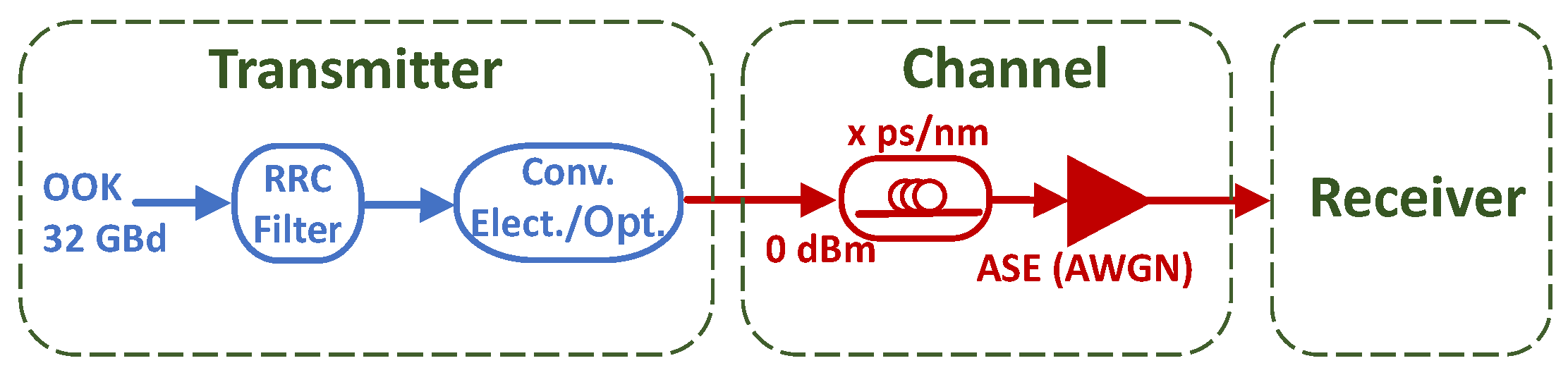
We propose the following system for short-reach communication. At the transmitter, a digital-to-analog converter (DAC) maps the signal to an OOK modulation format with root-raised cosine (RRC) as pulse shaping. We believe that our method can be easily extended to a PAM-4 modulation format, which will be considered in our future works. The Mach–Zehnder modulator (MZM) is used to modulate the signal. A standard single-mode fiber (SSMF) propagates the signal, and an erbium-doped fiber amplifier (EDFA) amplifies it. At the receiver, an optical band-pass filters the noise outside the signal bandwidth. Before detection, an optical module is used to pre-distort the signal to mitigate the CD. This process will be used to assist the nonlinear digital equalizer. A photodetector (PD) is then used to detect the signal, and an analog-to-digital converter (ADC) converts it to the digital domain. A DSP with NN equalizer and RRC filter are used to equalize the signal. The optical module, PD, and NN equalizer are the proposed hybrid optoelectronic blocks used to mitigate CD for direct detection systems.
Figure 1 shows the simulation setup used to validate the proposed system. At the transmitter, the DAC is the assumed ideal and an OOK 32-GBd signal is generated with
symbols, up-sampled to eight samples per symbol and filtered by a RRC filter (roll-off = 0.1). The digital signal is directly mapped onto the optical domain by assuming an ideal linear transformation. The MZM is assumed ideal in order to neglect its nonlinear transfer function as a source of degradation and to focus solely on the impact of CD. The CD (
D = 16.4 ps/nm/km) is the only impairment considered in the optical fiber, and additive white Gaussian noise (AWGN) is used to simulate the pre-amplifier at the Rx point. The noise variance and fiber length (accumulated CD) are swept to meet the target SNR and distance. The signal is then detected by a DD receiver.
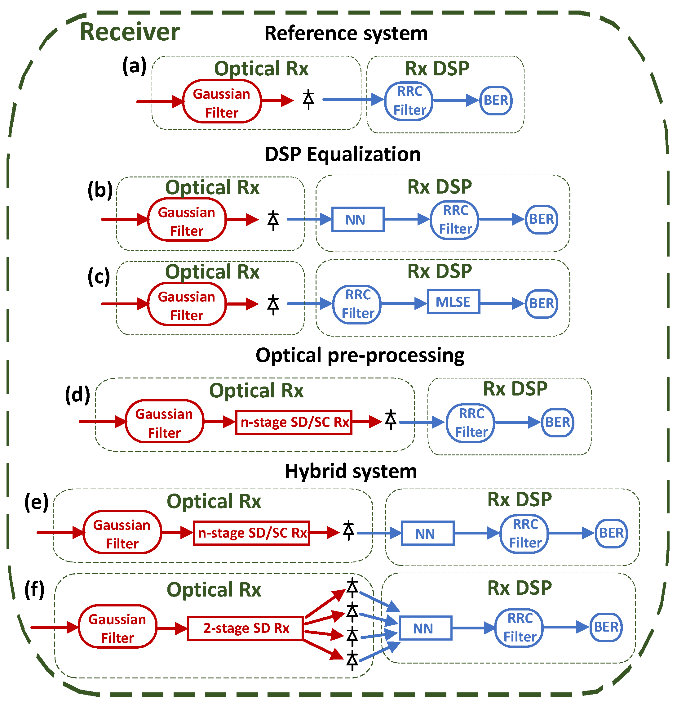
Figure 2 shows different topologies of the receiver that is analyzed in the result section. For all of them, a second-order Gaussian filter (40-GHz bandwidth) is used as a band-pass filter, which reduces the noise-to-noise beating in the PD. Moreover, the RRC filter block (ADC is assumed ideal) is used as a low-pass filter to downsample the signal to one sample per symbol. Receiver (a) is used as a reference. No optical pre-processing or digital equalization is applied. Receivers (b) and (c) show the block diagram for digital equalization with NN and MLSE (more details in
Section 2.2), respectively. Receiver (d) shows the block diagram for optical pre-processing using a complete optical module (more details in
Section 2.1). Receivers (e) and (f) show the proposed hybrid solution to mitigate CD. The former is based on the complete optical module, together with the NN. The latter is the receiver with the proposed simplified optical module together with an NN, respectively.
The simulation results firstly show a comparison between the performance of optical equalization and electronic equalization, individually. This results are followed by the complete hybrid module. Secondly, we analyze the requirements of the optical module to mitigate CD in a hybrid system. Thirdly, we compare a simplified hybrid module with the complete hybrid module. Fourthly, we study the tolerance of the simplified and complete hybrid module to CD. And lastly, we investigate the performance of NN in both hybrid systems.
2.1. Optical Pre-Processing
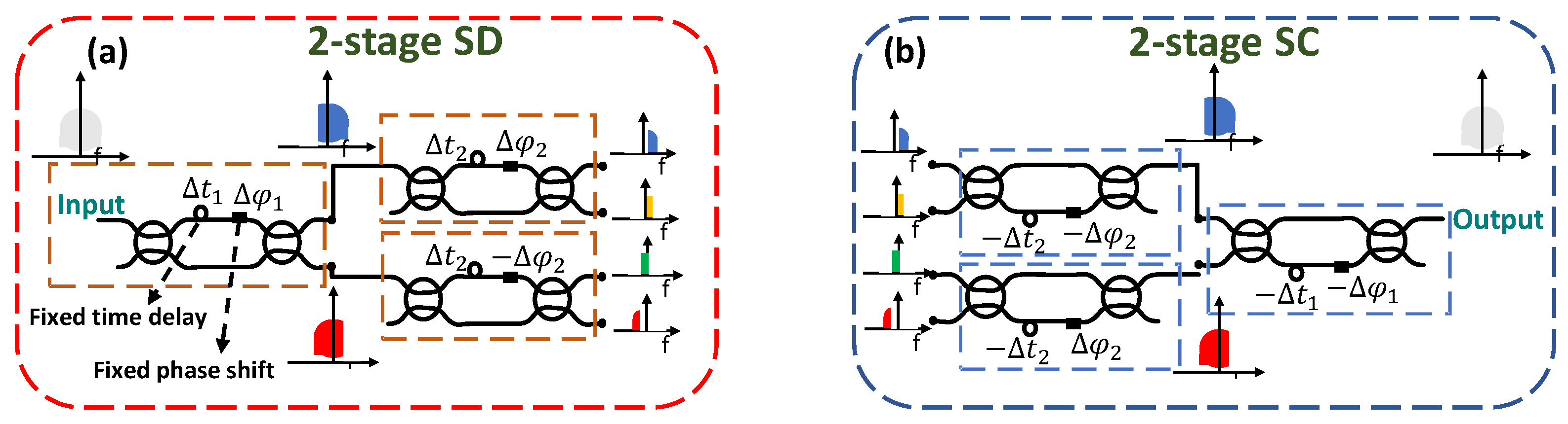
The optical module to mitigate the CD is based on the spectrum decomposition (SD) and spectral composition (SC) blocks [
17]. SD is a technique in which the signal is sliced into narrow frequency sub-bands. The basic building-block for this process is a phase-tunable Mach–Zehnder delay interferometer (MZDI).
Figure 3a is an example of a two-stage SD (four sub-bands). The orange dashed lines highlight the MZDI. The bandwidth of the sub-bands and the relative position of each other depends on the delay (
) and phase shift (
) of the MZDI.
i is the number of stages. Equations (1) and (2) describe it.
in which
is the angular frequency where the signal’s power is maximized in the output upper arm of the MZDI and minimized for the other. The inverse delay,
d, determines the distance in frequency where the maximum and minimum of the signal’s power is alternated in each output arm of the MZDI. For example, considering
rad/s and
GHz, the signal’s power is maximized at 12 GHz and alternates between minimum and maximum power every 8 GHz for the output upper arm, and the opposite for the lower arm. For a two-stage SD, we considered in the first stage
GHz and
rad/s. For the second stage we considered,
GHz and
rad/s.
SC applies the inverse transfer function of the SD, and it is highlighted in blue dashed lines in
Figure 3b. Perfect reconstruction of the signal is obtained if the SD is applied, followed directly by the SC. By knowing the transfer function of CD, a time delay and phase shift in each of the sub-bands of the SD can approach the inverse of the CD transfer function. The approximation increases in accuracy for increasingly narrower spectral slices. The values of the delay and phase depend on the number of sub-bands and the CD. The SD and SC structures, together with the delay and phase to mitigate the CD in each sub-band, is called the n-stage SD/SC Rx (
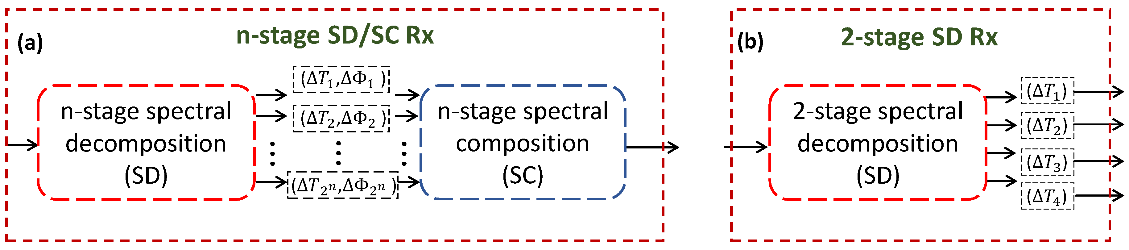
Figure 4a) in this work.
Figure 4 shows the optical pre-processing modules.
Figure 4a shows an n-stage SD/SC Rx, which is composed of
MZDI modules and creates
sub-bands.
Figure 4b shows a simplified version of the optical module. We are proposing to remove the SC part in the two-stage SD/SC structure. In this configuration, the optical module is acting as an optical pre-processing structure to assist the equalization process in the digital domain. The phase shift is not considered because the signal is directly connected to the PD. The different signals in the electrical domain need to be recombined and the equalizer can perform this operation implicitly. An addition of three PDs is necessary for receiving all four optical outputs of a two-stage SD. The performance of both optical modules is analyzed in the results section.
2.2. Digital Processing
Figure 5a shows a schematic of an NN equalizer [
18]. It is a two-layer NN, performing regression, with L neurons in the hidden layer and eight neurons in the output layer (one symbol). A hyperbolic tangent function is used as an activation function in the hidden layer, while a linear function is used in the output layer. The number of inputs of the NN depends on the optical module. If the n-stage SD/SC Rx is being analyzed, there are five symbols (40 samples) in the input. Otherwise, the number of input symbols are five per PD, which means 200 samples for the two-stage SD Rx. It is important to highlight that the middle symbol of the input is the one being equalized (symbol #3). In this way, the NN can take into account the symbols’ neighbors’ interference. The input window is shifted by a symbol period. The n-stage SD/SC Rx (
Figure 4a), together with the NN, is called in this work the hybrid n-stage SD/SC. The two-stage SD RX (
Figure 4b), together with the NN, is the hybrid two-stage SD.
The weights of NN, group delay, and phase of CD mitigation of the optical modules are jointly trained when these variables are available in the simulation. The algorithm to update them is the stochastic gradient descent with adaptive moment estimation [
19]. The loss function considered is the cross-entropy between the transmitted and received bits. During an entire simulation (
symbols), all the trainable variables are kept constant and they are only updated when the next simulation starts. All the variables are updated at the same time after 600 iterations of the training process.
Figure 5b shows an example of a decided 8-bit sequence with seven memory MLSEs. The MLSE “m” memory is an algorithm with
trellis states. The probability density function of the received sequence bits are first estimated, and then used to make the decision [
9].
3. Results
All the results are shown in terms of SNR penalty at KP4 FEC, with a hard-decision BER threshold of
[
20]. The SNR varies from 13 to 20 dB. Each simulation is repeated five times to measure the statistical relevance of the results.
3.1. Hybrid Signal Processing
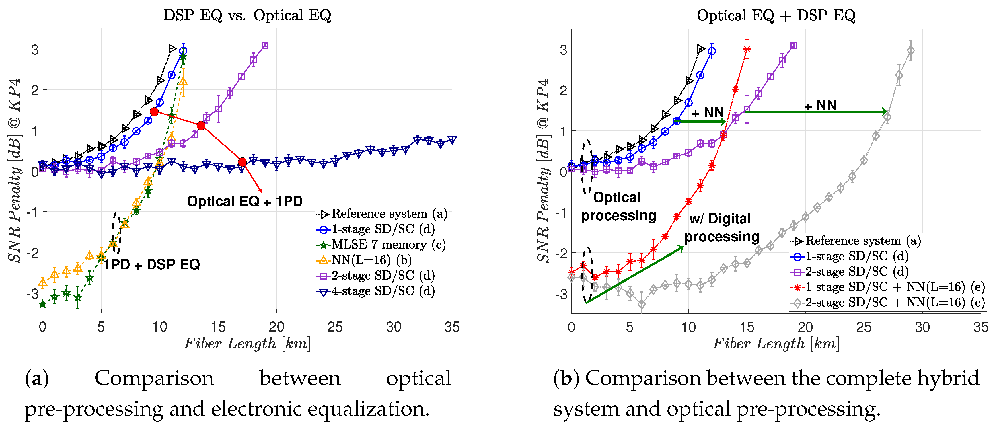
Figure 6 shows the results comparing the performance of a complete hybrid optoelectronic structure.
Figure 6a compares the optical and electronic equalization, individually. The black curve (right-side triangle) shows the result without optical or digital signal processing, namely our reference system. The blue (circle), purple (square), and dark blue (upside-down triangle) curves are the ones with only optical pre-processing. We note that increasing the number of stages in the n-stage SD/SC structure increases the maximum transmission reach. As we better compensate the CD, the narrow slices are required [
21]. Using four-stage SD/SC, a transmission of more than 574 ps/nm of accumulated CD (35 km of equivalent fiber) is demonstrated with less than 1 dB of SNR penalty at KP4, compared to a back-to-back transmission. The dark green (star) dashed line curve and yellow (upper triangle) dashed line curve are the digital processing for MLSE and NN, respectively. It is worth to point out that the seven-memory MLSE and the NN had similar performance. Using only electronic processing with an NN equalizer or MLSE, we showed a transmission of 164 ps/nm of accumulated CD (10 km of equivalent SSMF), considering a 0 dB SNR penalty at KP4 FEC compared to a back-to-back transmission. A difference between optical and digital performance can be clearly seen. As the phase is not accessible in the digital domain after the PD, such a difference appears [
8].
Figure 6b compares the complete hybrid optoelectronic system with optical equalization only. The red (asterisk) and grey (diamonds) show the result for the hybrid processing. We note that it is possible to further mitigate the CD and increase the transmission reach by adding post-processing in the digital signal part. This post-equalization is mitigating the residual CD of the system. In other words, instead of adding more stages in the SD/SC structure, which increases the optical complexity, it is possible to transfer part of this complexity to the digital domain.
Figure 6b shows an equivalent SSMF fiber transmission of 12 km (≈200 ps/nm) for a hybrid one-stage SD/SC module and 25 km (≈400 ps/nm) for a hybrid two-stage SD/SC module, considering a 0 dB penalty. Another observation is that the minimum SNR penalty is 0 dB for optical pre-processing, but less than 0 dB for electronic processing. This indicates that the optical module is trying to compensate only for the CD, while the electronic one is also trying to mitigate some of the effects of the square-law reception.
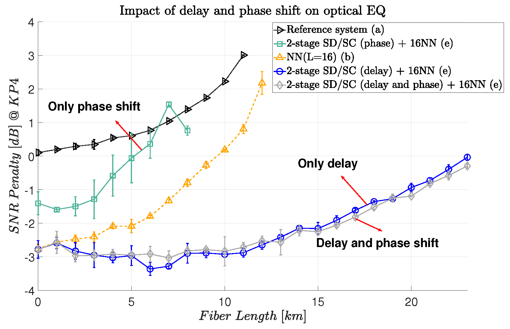
3.2. Delay and Phase Shift Impact on CD for Hybrid Two-Stage SD/SC
The CD transfer function shows that the modulated signal has a time delay and a phase shift effect during propagation. In this section, we investigate these effects considering the hybrid two-stage SD/SC structure.
Figure 7 shows these results. The blue curve (circle) shows the results achieved by applying only the time delay. The grey curve (diamond) shows the result of applying time delay and phase shift. These two curves show a similar performance, suggesting that the phase shift is not necessary. By applying only the phase shift (light green curve-square), instead, the performance worsens compared to using only digital equalization (yellow curve-upper triangle). We can, therefore, conclude that delay is the most significant operation in the hybrid module to mitigate CD.
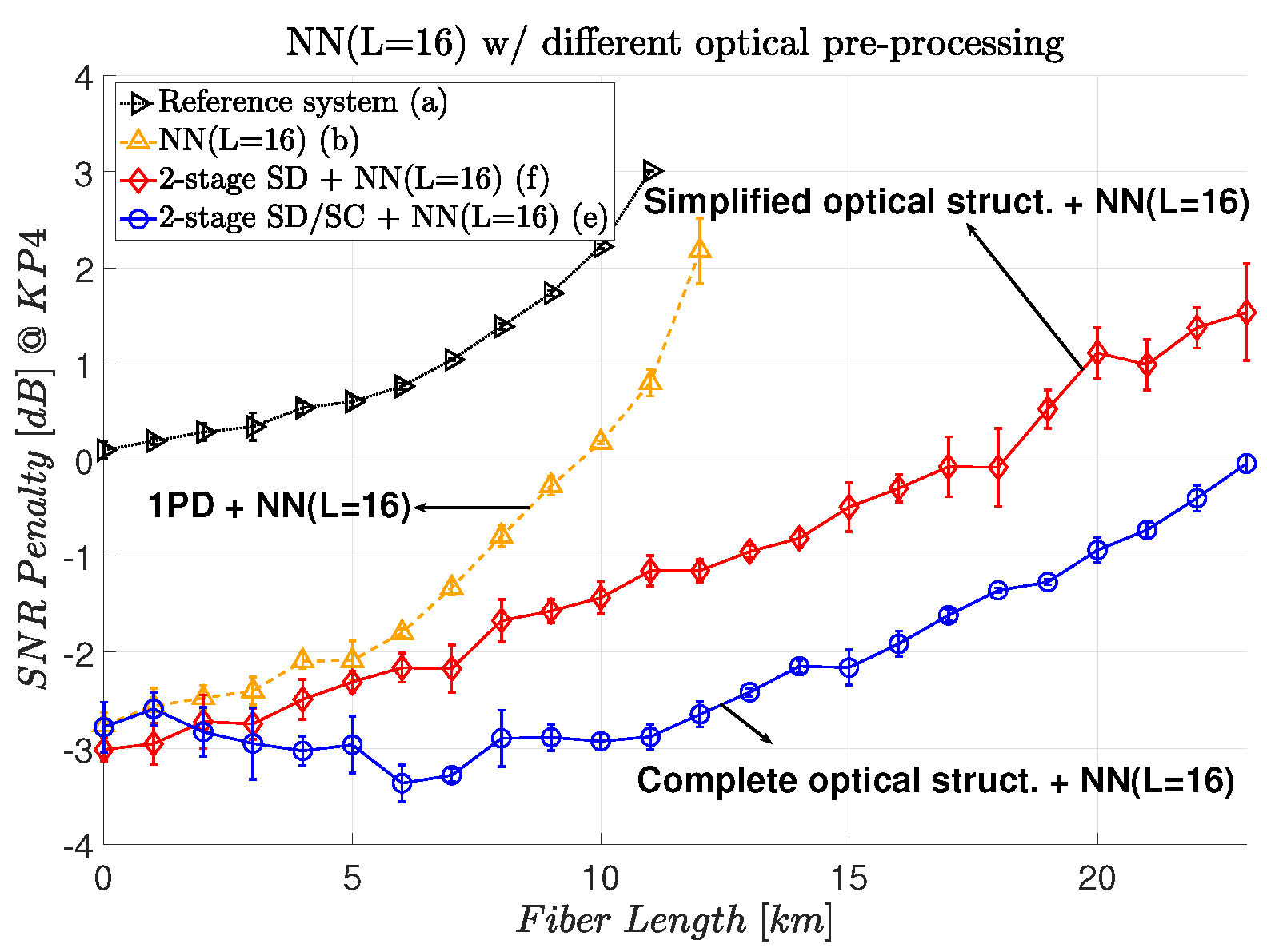
3.3. Simplified Hybrid Processing Performance
In this section, we investigate the effects of simplifying the optical module by implicitly transferring the SC operation to the nonlinear equalizer.
Figure 8 shows a comparison between the two-stage SD/SC and two-stage SD optical modules in a hybrid topology with an NN (L = 16). Without the SC structure, a two-stage SD module still mitigates the CD with ≈1.5 dB of the SNR penalty at KP4 FEC. We can also note that in the back-to-back transmission, there is almost no SNR penalty, which indicates that the NN is being able to regroup the four signals back into a single one.
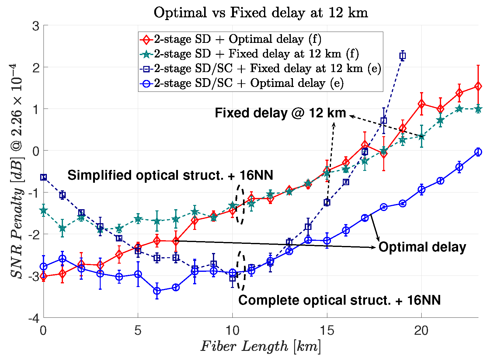
3.4. Delay Tolerance for Optical Hybrid Processing
One of the challenges of the proposed optical modules was finding the optimal delay to mitigate the CD. This happened because we used the stochastic gradient descent with adaptive moment estimation to update the delay and the weights of the NN at the same time. This can make the convergence process more difficult. To avoid this slow convergence and simultaneously simplify the optical structure, we investigated the performance of the hybrid systems for a fixed delay at 12 km of fiber transmission.
Figure 9 shows the tolerance to CD in this scenario. The hybrid two-stage SD has a CD tolerance similar to the case in which the optimal delay is calculated. In other words, almost no penalty is introduced by fixing the delay. In contrast, the hybrid two-stage SD/SC with fixed delay showed lower CD tolerance. This might be an indication that the sensibility in the delay of the full optical structure (SC/SD) is mainly related to the SC section.
Comparing both modules with a fixed delay and 0 dB SNR penalty at KP4 FEC, the hybrid two-stage SD/SC shows a transmission of ≈370 ps/nm of accumulated CD (23 km of equivalent SSMF). The hybrid two-stage SD shows a transmission of ≈300 ps/nm of accumulated CD (18 km of equivalent SSMF).
Considering only the hybrid two-stage SD, there was no penalty for the distance from 7 to 18 km. Below 7 km, the performance with a fixed delay was higher, which could indicate a missing interpolation operation from the NN to adapt to a better time delay. For distances from 18 to 23 km, we note that the fixed delay had less penalty. However, the curve with optimal delay showed a higher standard deviation, which indicates a more difficult convergence for the trainable variables. Fixing the delay would mean simplifying the convergence for the NN and, for this specific amount of CD, it showed better performance. Considering the hybrid two-stage SD/SC, we note that there was no penalty from 8 to 13 km. Outside this range, the penalty increased faster compared to the optimal delay.
3.5. Impact of the NN in Hybrid Processing
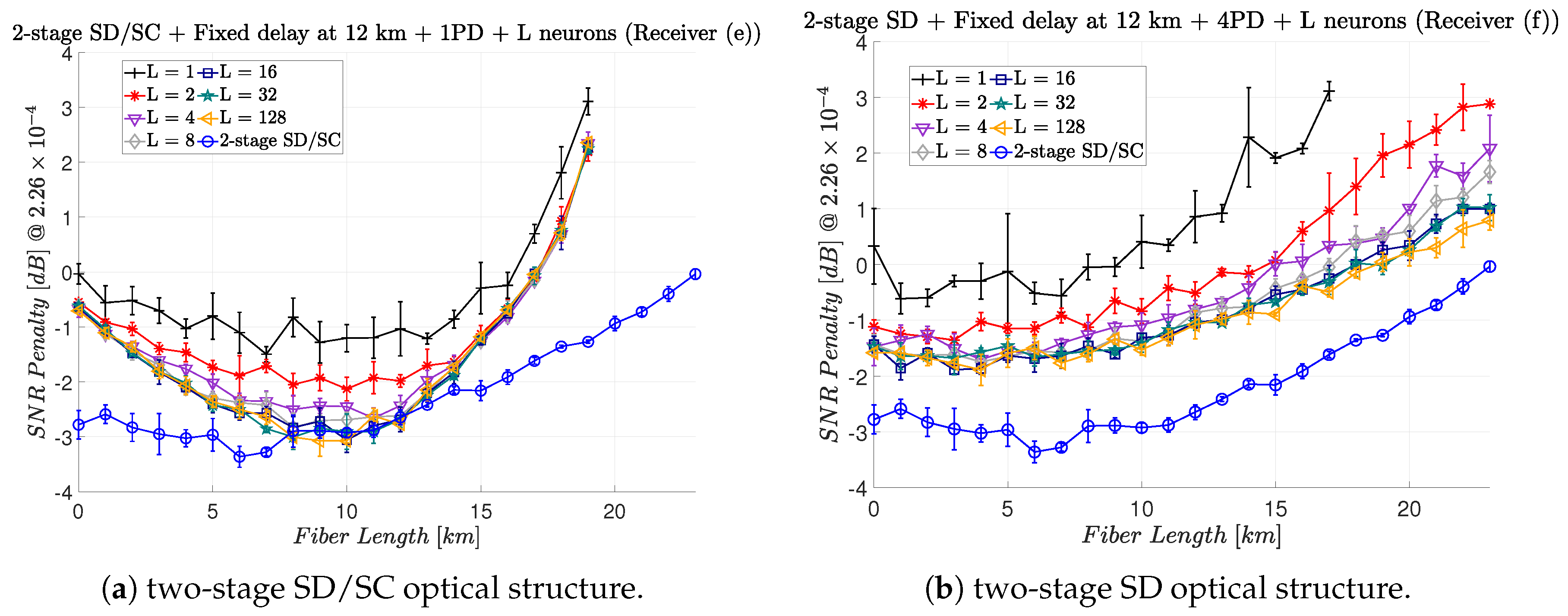
Figure 10 shows the impact of decreasing or increasing the number of neurons in the hidden layer for the NN.
Figure 10a,b show the results for the hybrid two-stage SD/SC and hybrid two-stage SD, respectively. The delay is fixed considering a 12 km transmission. As a reference, a hybrid two-stage SD/SC with 16 neurons in the hidden layer with optimal delay is shown.
Figure 10a shows that between 8 and 16 neurons is the optimal number of neurons in the hidden layer. For less than 8 neurons, the SNR penalty increases. For more than 16 we cannot see significant improvements. Although the NN could potentially find and adjust the optimal required delay, this is not happening even by increasing the number of neurons in the hidden layer. Increasing the number of neurons makes the convergence process more difficult.
Figure 10b also shows that the ideal number of neurons in the hidden layer is also between 8 and 16. Similar behavior as
Figure 10a for using less or more neurons is repeated here. Even considering the SNR penalty, using fewer neurons is still a possibility for the inter-data center scenario, because of the reduced complexity of the nonlinear equalizer.
4. Conclusions
In this paper, we showed a tuneable hybrid signal processing system to increase the maximum transmission reach for a DD system. Considering only the optical part of the hybrid module (n-stage SD/SC), we demonstrated that adjusting only the delay in the middle of the optical structure was sufficient to mitigate the CD. The more transmission reach was desired, the more optical complex structure is required. Using a four-stage SD/SC, a transmission of more than 574 ps/nm of accumulated CD (35 km of equivalent SSMF) was demonstrated with less than 1 dB of SNR penalty at KP4, compared to a back-to-back transmission.
Using only electronic processing with an NN equalizer or MLSE, we showed a transmission with 164 ps/nm (10 km of equivalent SSMF) of accumulated CD, in the same scenario. Adding the NN equalizer as post-processing in the hybrid module, we transferred part of the complexity from the optical to the electronic domain. For a one-stage hybrid module (one-stage SD/SC + NN (L = 16)), we showed a CD mitigation of ≈200 ps/nm (12 km of equivalent standard single-mode fiber length). The tolerance was roughly doubled for a two-stage hybrid module (two-stage SD/SC + NN (L = 16)). Removing the SC from the hybrid structure (two-stage SD + NN (L = 16)) reduced the optical complexity module without losing the capacity of mitigating the CD. However, there was a ≈1.5 dB penalty compared to a complete two-stage hybrid module.
A key component to mitigate the CD in the optical modules is the time delay. We showed that it is possible to keep this delay constant for a specific range of transmission reach and simplify the optical structure. For the two-stage hybrid module and considering 0 dB SNR penalty at KP4 FEC compared to a back-to-back transmission, we showed a transmission with an accumulated CD of ≈370 ps/nm (23 km of equivalent SSMF) using the time delay for a 12 km transmission. For the hybrid two-stage SD, the proposal module, there was no penalty by fixing the time delay. At the same scenario, we showed a transmission with accumulated CD of ≈300 ps/nm (18 km of equivalent SSMF). Finally, we analyzed the required number of neurons in the hidden layer of the NN. For both structures, the ideal number calculated was between 8 and 16 neurons.
Author Contributions
Conceptualization, S.M.R., F.D.R., H.B. and D.Z.; Investigation, S.M.R.; Supervision, F.D.R., H.B. and D.Z.; Validation, S.M.R.
Funding
This project has received funding from the European Union’s Horizon 2020 research and innovation programme under the Marie Skłodowska-Curie grant agreement No 766115. It is also supported by the European Research Council through the ERC-CoG FRECOM project (grant agreement no. 771878).
Conflicts of Interest
The authors declare no conflict of interest.
References
- Agrawal, G.P. Fiber-Optic Communication Systems, 3rd ed.; John Wiley & Sons: Hoboken, NJ, USA, 2002. [Google Scholar]
- Turkiewicz, J.P. Cost-effective n× 25 Gbit/s DWDM transmission in the 1310 nm wavelength domain. Opt. Fiber Technol. 2011, 17, 179–184. [Google Scholar] [CrossRef]
- Cheng, J.; Xie, C.; Chen, Y.; Chen, X.; Tang, M.; Fu, S. Comparison of Coherent and IMDD Transceivers for Intra Datacenter Optical Interconnects. In Proceedings of the Optical Fiber Communications Conference and Exhibition (OFC), San Diego, CA, USA, 3–7 March 2019. [Google Scholar]
- Chagnon, M. Direct-detection Technologies for Intra-and Inter-Data Center Optical Links. In Proceedings of the Optical Fiber Communications Conference and Exhibition (OFC), San Diego, CA, USA, 3–7 March 2019; pp. 1–41. [Google Scholar]
- Zhou, H.; Li, Y.; Liu, Y.; Yue, L.; Gao, C.; Li, W.; Qiu, J.; Guo, H.; Hong, X.; Zuo, Y.; et al. Recent Advances in Equalization Technologies for Short-Reach Optical Links Based on PAM4 Modulation: A Review. Appl. Sci. 2019, 9, 2342. [Google Scholar] [CrossRef]
- Zhong, K.; Zhou, X.; Huo, J.; Yu, C.; Lu, C.; Lau, A.P.T. Digital signal processing for short-reach optical communications: A review of current technologies and future trends. J. Lightwave Technol. (JLT) 2018, 36, 377–400. [Google Scholar] [CrossRef]
- Jignesh, J.; Eriksson, T.A.; Chagnon, M.; Corcoran, B.; Lowery, A.J.; Buchali, F.; Bülow, H. Transmitter-side Volterra filtering for increased dispersion tolerance in 56 Gbaud PAM-4 systems. In Proceedings of the Optical Fiber Communications Conference and Exhibition (OFC), San Diego, CA, USA, 11–15 March 2018. [Google Scholar]
- Rubsamen, M.; Gene, J.M.; Winzer, P.J.; Essiambre, R.J. ISI mitigation capability of MLSE direct-detection receivers. IEEE Photonics Technol. Lett. (PTL) 2008, 20, 656–658. [Google Scholar] [CrossRef]
- Agazzi, O.E.; Hueda, M.R.; Carrer, H.S.; Crivelli, D.E. Maximum-likelihood sequence estimation in dispersive optical channels. J. Lightwave Technol. (JLT) 2005, 23, 749–763. [Google Scholar] [CrossRef]
- Qian, H.; Mathieu, C.; Karsten, S.; Fred, B.; Henning, B. High Data Rate Tomlinson-Harashima precoding-Based Pam Transmission. In Proceedings of the European Conference on Optical Communication (ECOC), Dublin, Germany, 22–26 September 2019. [Google Scholar]
- Mecozzi, A.; Antonelli, C.; Shtaif, M. Kramers–Kronig coherent receiver. Optica 2016, 3, 1220–1227. [Google Scholar] [CrossRef]
- Mardoyan, H.; Jorge, F.; Baeuerle, B.; Estaran, J.M.; Heni, W.; Konczykowska, A.; Riet, M.; Duval, B.; Nodjiadjim, V.; Goix, M.; et al. 222-Gbaud On-Off Keying Transmitter Using Ultra-High-Speed 2:1-Selector And Plasmonic Modulator On Silicon Photonic. In Proceedings of the European Conference on Optical Communication (ECOC), Dublin, Germany, 22–26 September 2019. [Google Scholar]
- Gaiarin, S.; Pang, X.; Ozolins, O.; Jones, R.T.; da Silva, E.P.; Schatz, R.; Westergren, U.; Popov, S.; Jacobsen, G.; Zibar, D. High speed PAM-8 optical interconnects with digital equalization based on neural network. In Proceedings of the Asia Communications and Photonics Conference (ACP), Wuhan, China, 2–5 November 2016. [Google Scholar]
- Chagnon, M.; Karanov, B.; Schmalen, L. Experimental demonstration of a dispersion tolerant end-to-end deep learning-based im-dd transmission system. In Proceedings of the European Conference on Optical Communication (ECOC), Roma, Italy, 23–27 September 2018; pp. 1–3. [Google Scholar]
- Katumba, A.; Yin, X.; Dambre, J.; Bienstman, P. A Neuromorphic Silicon Photonics Nonlinear Equalizer For Optical Communications With Intensity Modulation and Direct Detection. J. Lightwave Technol. (JLT) 2019, 37, 2232–2239. [Google Scholar] [CrossRef]
- Ranzini, S.M.; da Ros, F.; Zibar, D. Joint low-complexity opto-electronic chromatic dispersion compensation for short-reach transmission. In Proceedings of the IEEE Photonics Conference (IPC), San Antonio, TX, USA, 30 September–3 October 2019; pp. 1–2. [Google Scholar]
- Hillerkuss, D.; Schmogrow, R.; Schellinger, T.; Jordan, M.; Winter, M.; Huber, G.; Vallaitis, T.; Bonk, R.; Kleinow, P.; Frey, F.; et al. 26 Tbit s- 1 line-rate super-channel transmission utilizing all-optical fast Fourier transform processing. Nat. Photonics 2011, 5, 364. [Google Scholar] [CrossRef]
- Chen, S.; Gibson, G.; Cowan, C.; Grant, P. Adaptive equalization of finite non-linear channels using multilayer perceptrons. Signal Process. 1990, 20, 107–119. [Google Scholar] [CrossRef]
- Kingma, D.P.; Ba, J. Adam: A method for stochastic optimization. arXiv 2014, arXiv:1412.6980. [Google Scholar]
- Agrell, E.; Secondini, M. Information-theoretic tools for optical communications engineers. In Proceedings of the IEEE Photonics Conference (IPC), Reston, VA, USA, 30 September–4 October 2018; pp. 1–5. [Google Scholar]
- Slim, I.; Mezghani, A.; Baltar, L.G.; Qi, J.; Hauske, F.N.; Nossek, J.A. Delayed single-tap frequency-domain chromatic-dispersion compensation. IEEE Photonics Technol. Lett. (PTL) 2012, 25, 167–170. [Google Scholar] [CrossRef]
© 2019 by the authors. Licensee MDPI, Basel, Switzerland. This article is an open access article distributed under the terms and conditions of the Creative Commons Attribution (CC BY) license (http://creativecommons.org/licenses/by/4.0/).


