1. Introduction
Recently, photonic integrated circuits have been intensively investigated for applications in quantum photonics [
1], optical interconnection [
2], photonic computing [
3], and optical communications [
4]. Integration of multiple photonic components on a photonic chip requires the development of on-chip photonic integrable components, including waveguides, filters, and optical power splitters. An integrated optical power splitter is an important photonic building block that divides optical power into multiple channels, forms interferometer systems, and taps a small portion of signal [
5].
Several approaches have been developed for on-chip power dividers, including Y-junctions [
6], directional couplers [
7,
8], and multimode interferometers [
9,
10]. Conventional Y-junctions typically have a 1-dB insertion loss and a 3-dB splitting ratio due to fabrication imperfections [
11,
12]. In the case of directional couplers, the power splitting can be designed by controlling the coupling length and distance between the two waveguides, but the coupling ratio strongly depends on the input wavelengths [
8,
13]. Recently, curved directional coupler and its combination with straight directional couplers show small footprints, low loss, and ultra-broadband power splitting, but they need careful design in coupling regions [
14,
15]. Multimode interferometers not only have several advantages, such as relatively small size and high fabrication tolerances, but also have drawbacks, such as wavelength dependence and insertion loss [
9,
16]. Since the subwavelength grating can engineer refractive index and dispersion properties, a compact, low loss, and ultra-broadband directional couplers are proposed using its design flexibility [
17,
18,
19], but the gratings are intrinsically sensitive to fabrication errors. Furthermore, a 3-dB beam splitter that uses adiabatically tapered waveguides was demonstrated [
20] having a low insertion loss (<0.2 dB), a short coupling length (5 μm), and negligible dependency on the input wavelengths, but it has a fixed power split ratio of 50%. Even if these types of on-chip power splitters meet some of the performance requirements, it is a big challenge that an on-chip optical power splitter satisfies all of compactness, low-insertion loss, wavelength independence, and tailorability of the split ratio.
These properties are required not only in classical photonic signal processing but also in quantum photonics. For instance, in quantum photonic integrated circuits, asymmetric interferometers are used to generate time-bin entanglement, but a non-3-dB power splitter is needed due to propagation loss in longer path [
21]. In addition, controlled-NOT gate was demonstrated using directional couplers with 50:50 and 70:30 ratios [
3]. However, as the directional couplers used in these experiments have considerable wavelength dependence, precise control of fabrication is required.
In this work, we propose a novel scheme of on-chip photonic power splitters that can meet all the required characteristics of tailorability, wideband, compactness, and low insertion loss. The designed structure is based on 1 × 2 interleaved tapered waveguides (1 × 2 ITW) on a silicon-on-insulator platform, and a power split ratio can be determined by moving laterally one of the output tapered waveguides, lithographically. An insertion loss extracted from computational simulation results is less than 0.3% even if the split ratio changes from 50% to 1%, and wavelength dependence of the split ratio, as well as the insertion loss, is negligible in the wavelength range from 1.5 μm to 1.6 μm. This scheme is close to impeccable power splitters and can be the most promising photonic power divider for photonic integrated circuit systems and quantum photonics.
2. Materials and Methods
The simulations are performed by Lumerical’s MODE solution, which offers the 2.5D finite-difference time-domain method. The mesh accuracy used in the simulation is the predefined value 6 in Lumerical, which is small enough for the narrow tips in the tapered region in
Figure 1. The time step is about 0.04 fs. The boundary conditions are the perfect matched layer condition in the
x- and
y-directions and the metal boundary condition in the
z-direction. This metal boundary condition can reduce the simulation time and does not affect the simulation results as light is tightly confined in the waveguides.
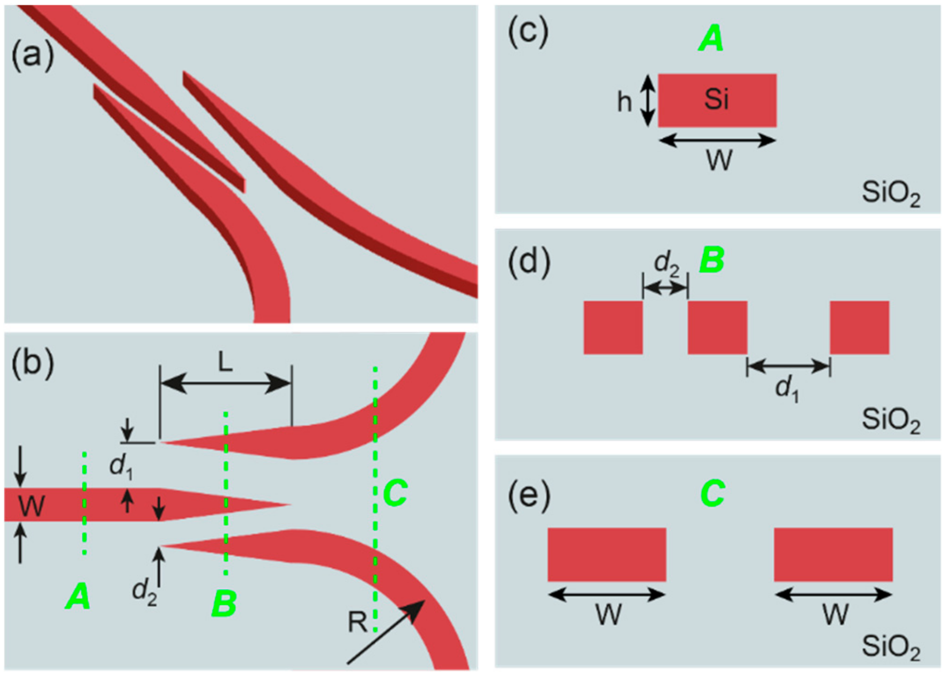
A 3D diagram of the proposed beam splitter is illustrated in
Figure 1a, and the top-down view of the power splitter system with various geometric parameters is shown in
Figure 1b. The 1 × 2 interleaved tapered waveguide (ITW) structure consists of an input port with one tapered waveguide and two output ports with tapered waveguides next to the input channel in the opposite direction. The waveguides are tapered in from 400 nm to 30 nm across the coupling length L (15 μm), as shown in
Figure 1b. Since the tapering angle of the input and output waveguides is identical, two slot waveguides are created, approaching each other along the propagation direction. The minimum tapering size of 30 nm is determined from typical and affordable electron beam lithography resolution. Divided optical power comes through two curved waveguides with a bending radius of 30 μm. The cross-sectional views of the power splitter system at locations A, B, and C in
Figure 1b are shown in
Figure 1c–e, respectively. The silicon waveguides in this scheme are surrounded by a SiO2 cladding and have a thickness (
h) of 220 nm and a width (W) of 400 nm, as seen in
Figure 1c–e.
The performance of this structure is simulated for various geometrical conditions. The gap size between the input tapered waveguide and the upper output waveguide in
Figure 1b varies lithographically from d
1 = 150 nm to 600 nm. By means of changing this gap d
1, the output ratio can be designed to achieve a desired split ratio. The lower gap of d
2 = 150 nm and the coupling length of L = 15 μm are fixed. The gap sizes d
1, d
2 and the coupling length L are larger than those in reference [
20]. The gap size of 150 nm is slightly larger than the decaying depth of the evanescent wave. The gap size of less than 150 nm can yield complicated coupling between waveguides due to long evanescent tails, and the power splitting becomes sensitive to fabrication errors. The gap size of 150 nm is large enough to prevent complicated coupling and to achieve tailorable power relatively readily. On the other hand, simulation results show that a beam splitter with larger gap size than d
1 = d
2 = 150 nm and shorter coupling length than L = 15 μm significantly increases its insertion loss. With the optimized gap size of 150 nm, the coupling length should be at least 15 μm to achieve transition with the fundamental mode and to compensate the loss induced by the large gap.
Note that this method is designed with only one polarization direction in silicon waveguides. The computational simulation is conducted with only transverse electric (TE)-like modes as many photonic integrated circuits support one polarization mode (mostly TE-like mode). In addition, transverse magnetic (TM)-like modes in this scheme have a higher loss, larger wavelength dependence, and a different splitting ratio with TE-like modes.
3. Results
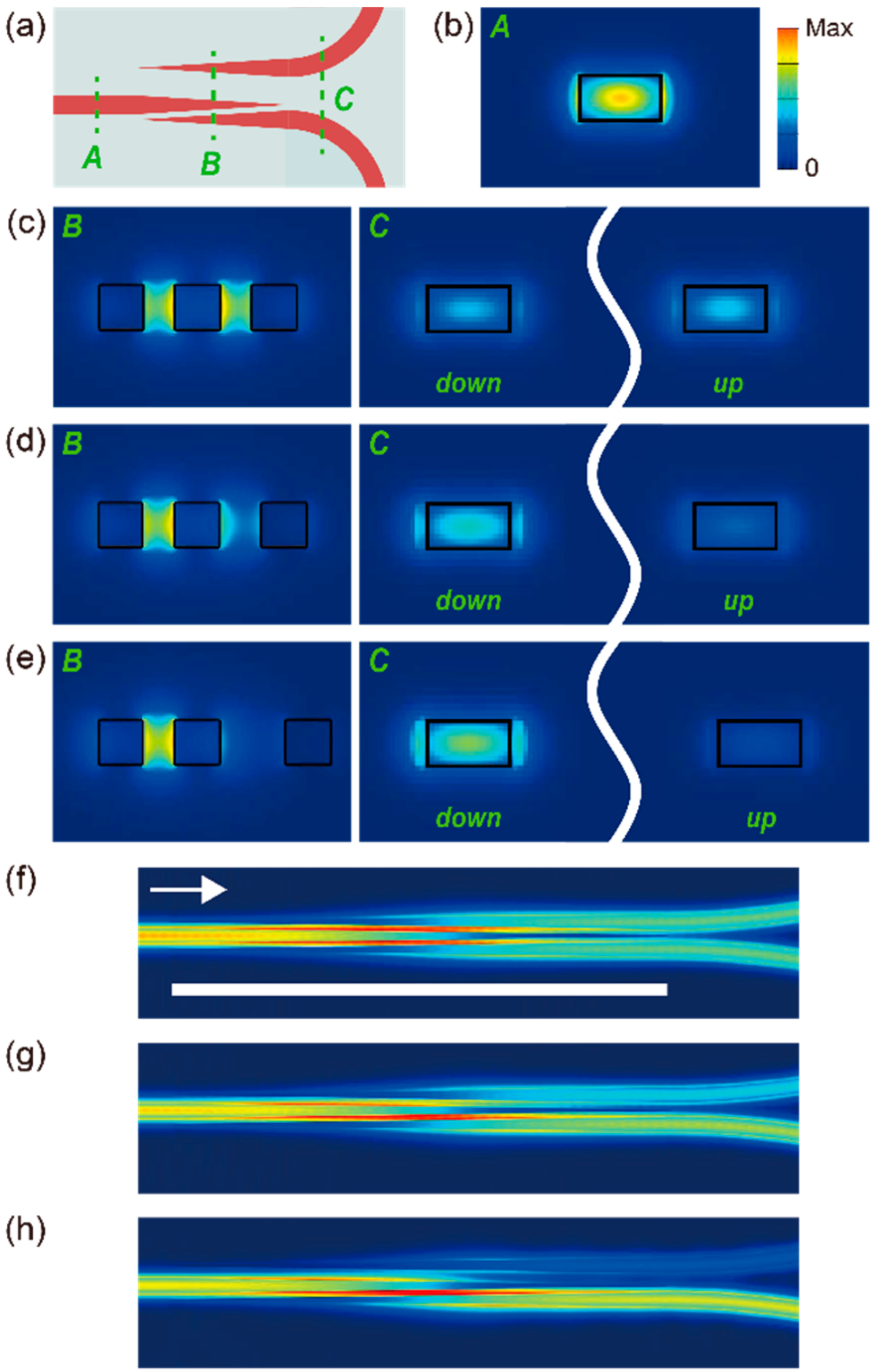
Power splitting behaviors in the TE-like mode are presented in
Figure 2. The cross-sectional view of the electric field intensity profile of the fundamental TE-like mode at position A of
Figure 2a is shown in
Figure 2b. The cross-sectional views of the fundamental electric field intensity profiles at location B and C for various upper gap sizes (d
1 = [150 nm, 200 nm, 315 nm]) are seen in
Figure 2c–e, respectively. Note that all the intensity profiles in
Figure 2 are normalized with a constant to emphasize the optical power splitting results. The lower gap size is fixed at 150 nm. The top-down views of the power flux density for various d
1 gap sizes are seen in
Figure 2f–h, and the extracted output power ratios are (
f) 50:50, (
g) 70:30, and (
h) 90:10 at d
1 = [150 nm, 200 nm, 315 nm], respectively.
From the boundary conditions of Maxwell’s equations, the discontinuity of the electric fields at the boundaries of two adjacent waveguides amplifies the electric field in the gap, referred to as a slot waveguide mode [
22]. Therefore, input light arriving at the coupling region slowly converges to double slot waveguide mode, as seen in the left-hand figures of
Figure 2c–e. These show the fundamental modes of the electric field intensity profile at the cross section B in
Figure 2a. At the end of the coupling section the electric field is strongly confined to the two output waveguides, splitting the optical power as a function of the gap size, d
1. The right-hand figures of
Figure 2c–e show the intensity profile of the two output ports at section C of
Figure 2a, proving that the optical power through the upper (lower) output port decreases (increases) as enlarging the upper gap size, d
1.
In the coupling region, in order to avoid the excitation to higher modes, it is required to maintain a large difference between the effective index of fundamental and secondary modes. The width of input/output waveguides is optimized to 400 nm in order to keep the index difference with low propagation and bending loss [
20]. However, in our scheme, the asymmetry structure by d
1 ≠ d
2 and the large gap size reduce the effective index difference between the fundamental mode and the higher modes, but the excitation to unwanted higher modes can be prevented by designing the coupling length [
23]. To maintain the fundamental mode transition, the coupling length of 15 μm is determined from the careful simulations.
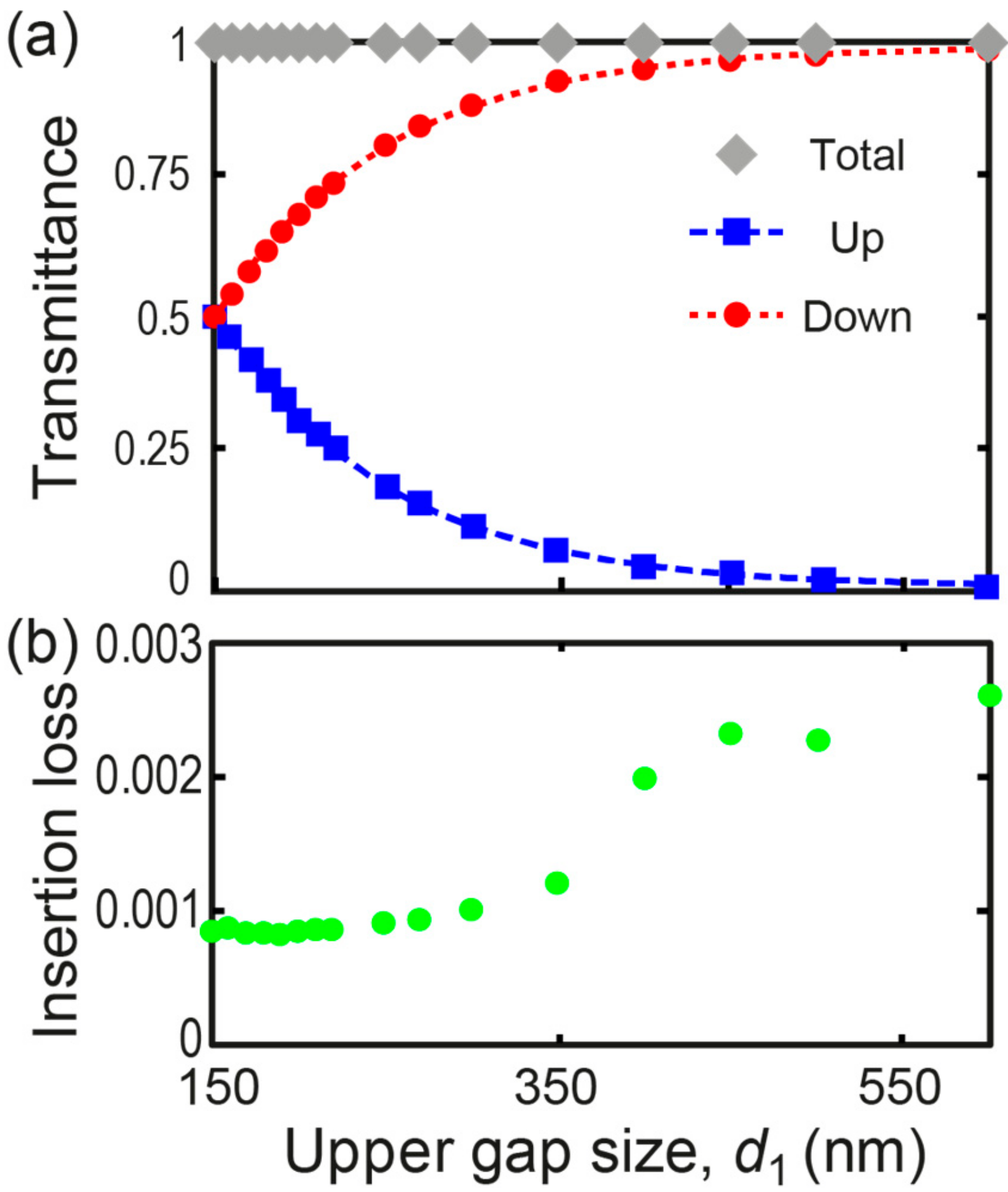
A beam splitter with a specific power ratio can be designed by controlling the upper gap size. In
Figure 3a, the simulation results of the transmittance through the upper, lower, and the total output channels are shown for the upper gap size. As the upper gap size increases, the coupling with the upper (lower) output waveguide exponentially decreases (increases) at the same rate, respectively. The coupling ratio is defined as
. Based on the simulation results in
Figure 3a, an upper gap size d
1 for a desired coupling ratio R with a fixed lower gap size d
2 = 150 nm is given by
where the coupling ratio R has a value between 0.004 and 0.5 and this equation is quoted for d
1 in nanometers. This equation can be used to determine an upper gap size for a desired coupling ratio. For example, to design a 90:10 beam splitter, the coupling ratio should be R = 0.1, and the required upper gap size is d
1 = 315 nm with a fixed lower gap size of d
2 = 150 nm.
Figure 3b shows the simulated insertion loss of the structure,
. By increasing the upper gap size from 150 nm to 600 nm, the insertion loss increases from 0.1% to 0.25% (~0.01 dB), which is negligibly low considering fabrication imperfections. In practice, light scattering from side-wall surfaces or fabrication error will be the dominant loss mechanisms.
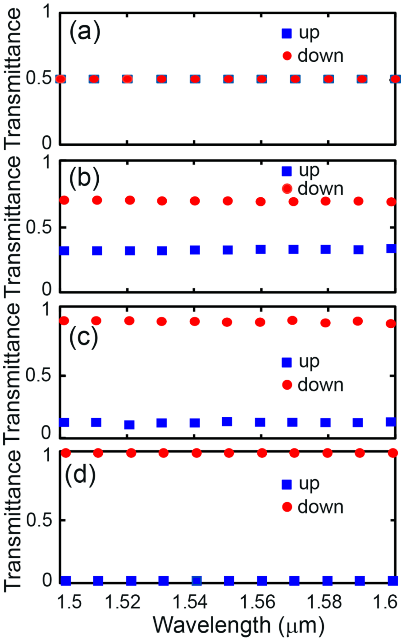
Figure 4 shows the transmittance through the upper and lower channels against input wavelength. The computational simulation is performed over a wavelength range of 1.5 μm to 1.6 μm for various upper gap sizes (d
1 = [150 nm, 200 nm, 315 nm, 590 nm]) corresponding to the power splitting ratios of 50:50, 70:30, 90:10, and 99:1, respectively. The simulated power split ratio has a deviation of less than 6.5% from its desired value within the overall simulation wavelength range. The profile of evanescent waves depends on the input wavelength, which may cause wavelength dependence. To reduce wavelength dependence, the lower gap size is optimized to 150 nm, which is larger than the characteristic decaying length of the input light but small enough to support slot waveguide modes with weak wavelength dependence. The larger gap size reduces wavelength dependence, but leads to high optical power leakage.
The coupling ratio deviation is defined by
, and the maximum deviations in wavelength range between 1.5 μm and 1.6 μm (1.2 μm–1.8 μm) are 0.49% (2.54%) for 50:50, 2.85% (12.30%) for 30:70, 0.27% (7.11%) for 10:90, and 0.86% (1.20%) for 1:99. Due to the slowly varying material refractive index in wavelength, the evanescent profile, as well as the splitting ratio, change slowly in wavelength. However, even in 1.2 μm–1.8 μm range, the maximum deviation is about 10%, showing ultra-broadband tailorability compared to recent methods of broadband power splitters [
14,
18].
4. Discussion
Note that the geometry of the proposed system has typical size values and materials that are used in common photonic integrated circuit technologies. The input and output waveguides can be readily fabricated using excimer laser photolithography, but the feature size of 30 nm at the tapering tips is too small for typical photolithography. Electron beam lithography is one way to obtain such a resolution, but it is not a cost effective way. Alternative method is hybrid lithography where photolithography is used for the entire waveguide system and electron beam lithography is used only for the high-resolution region [
24].
The waveguide width can be slightly reduced or enlarged by fabrication error, which can result in a different beam-splitter-gap size from its original design. In our scheme, the output split ratio is determined by the relative gap size between the upward and the downward waveguide. If all waveguides shrink or expand in the same way, the difference between the two gap sizes would not change, maintaining the split ratio. To test the effect of this transformation on the splitting ratio, we repeat the computational simulations with an acceptable waveguide width tolerance of ± 10 nm in electron beam lithography. From the simulation results, the transmittance of the output changes by up to 1% from the desired splitting ratio values, which can be negligible. This result shows that our optical power splitter scheme is robust to this type of fabrication errors. In addition, when the width or height of the input/output waveguides needs to change under certain experimental conditions, the size of the gap and the selection equation of a power splitting ratio should slightly differ from the current state. Designing a precise beam splitter, though not strictly necessary, should be considered with new conditions.
In this simulation, only the TE mode is considered. In the TM mode, the evanescent electric field exists at the top and bottom of the waveguides, and the mode profile in the coupling region is complicated and very sensitive to wavelength and geometry dimension variance. In relevant simulations, we observe that the relationship between the gap size and power splitting ratio in the TM mode is different from Equation (1) and is not as simple as that in the TE mode case. We could not find a meaningful and straightforward expression of the relationship as the ratio is too sensitive to the gap size. In addition, we consider the linear optical properties of the proposed design by excluding the nonlinear absorption, power-dependent refractive index, and thermal heating. Further research about the nonlinear optical behaviors of this device is needed.
Recently, other materials, such as silicon nitride, aluminum nitride, and lithium niobate, are intensively investigated in the fields of photonic integrated circuits. Our suggested structure can be employed not only in silicon but also in other platforms. Due to the different refractive index, mode size, and evanescent profile on other platforms, the parameters in Equation (1) differ from those in silicon than silicon, and further research is required.


