Abstract
We explore the monolithic integration of conventional electronics with SOI photonics using the commercial silicon photonics foundry technology offered by A*STAR’s Institute of Microelectronics (IME). This process offers optical waveguide modulators and photodetectors, but was not intended to support transistors. We present the implementation of junction field effect transistors (JFETs) integrated with optical waveguides and photodetectors. A simple SPICE model is developed for the JFETs based on the available ion implant parameters, and the geometry feature size allowed by the technology’s layout rules. We have demonstrated the monolithic integration of photonics and electronics circuits. This work could be useful for application in waveguide sensors and optical telecommunications.
1. Introduction
Conventional complementary metal oxide semiconductor (CMOS) technology has been the most important technology for the fabrication of microelectronic circuits for decades. The hybrid (non-monolithic) integration method has been employed during its development. However, monolithic microelectronics integrated with silicon photonics offers advantages in terms of improved signal-to-noise ratio, reduced parasitic capacitance, better reliability, and lower transmission cross-talk. Unfortunately, at the time of project fabrication, there is no public access to commercial foundries for the monolithic integration of full CMOS microelectronics and photonic components, even though several companies including Intel, Luxtera, and IBM have such technologies available for their internal use. For example, IBM developed a silicon photonic transmitter for next-generation short-reach optical interconnects. This is the first demonstration of a fully monolithically integrated silicon photonic four-level pulse amplitude modulation (PAM) transmitter, operating at 56 Gb/s with error-free transmission [1]. Most recently, 45-nm and 32-nm SOI CMOS circuits were fabricated on a “zero-change” silicon photonics platform by the IBM/Global Foundries, demonstrating monolithic silicon photonic platforms in the state-of-the-art CMOS SOI processes [2]. In order to achieve electronic transistors integrated with photonic devices, we have therefore investigated the realization of junction field effect transistors (JFETs) in a foundry SOI photonics technology, which is offered by A*Star’s Institute of Microelectronics (IME) (Singapore). Although the silicon MOSFET is a workhorse device of modern electronic design, JFETs have their unique advantages: very low current noise, high input impedance, insensitivity to temperature, and immunity to radiation. Hence, JFETs are widely used as input amplifiers in oscilloscopes, electronic voltmeters, and other measuring and testing equipment [3]. They are also an excellent choice for monolithic integration with photodetectors on an SOI platform. For example, n-channel JFETs were integrated with silicon PIN detectors for biomedical applications reported in [4,5,6]. In addition, the epitaxial growth of JFETs was also developed for monolithic photoreceiver integration [7,8]. In this work, we have focused on designing and demonstrating the monolithic integration of electronic transistors (JFETs) with photonic components. We have also concentrated on devices suitable for sensor integration, in part because many important applications of SOI-based photonic sensing are under development, but also because the speed requirements of sensors are usually much more relaxed than those needed in telecommunications. However, with the availability of more advanced lithography than was available for this project, the techniques and devices developed in this work could be extended to telecommunications or data communication applications.
2. JFET Design and Characteristics
We use the IME Silicon Electronic Photonic Integration Circuit (SiEPIC) technology to achieve the photonic and electronic integration. The process is intended for the integration of passive photonic devices (waveguide, grating couplers, multiplexer, etc.) and active photonic devices (modulators, Ge photodiodes, resonators, etc.) onto a monolithic chip. Various n-type and p-type ion implants for pn junction formation used in optical modulators and epitaxial Ge photodetectors are available [9]. It starts with a sequence of selective etching, hard mask deposition, waveguide formation, ion implants for modulators and photodetectors, Ge epitaxy, Ge top implant, and ends with metal connections and bond pads. Although the process was not intended to create transistors, it occurred to us that these implants could be used to create JFETs that could be used in transimpedance amplifiers and other circuits. We estimated the doping and dimensions for each active region of the JFET based on the given implant dosages and energies, the Si film thicknesses offered by the process, and the minimum feature sizes allowed by the design rules. The implants could also be used to implement lateral bipolar junction transistors (LBJTs), but our previous experiments indicated the maximum LBJT common-emitter current gain is less than unity, and therefore, these devices do not provide useful amplification [10].
The perspective view of the n-JFET structure is shown in Figure 1 [3]. An n-channel device is used since the electron mobility in silicon is roughly three times that of holes. Two ohmic contacts are connected at the ends of the channel, with one acting as the source and the other as the drain. When a positive voltage is applied to the drain with respect to the source, electrons flow from the source to the drain. Two electrically connected p+ regions on both sides of the channel form the gate. Here, the device width Z is 10 µm, and the length L is 18 µm. The gate-channel width 2a is 0.8 µm, and the depth d is 0.22 µm. A reverse bias applied to the gate channel pn junction widens the junction depletion region, modulating the width of the undepleted channel, and hence controlling the current flow between the source and drain.
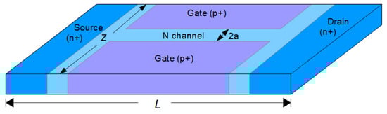
Figure 1.
Perspective view of an NJFET.
SPICE model parameters were calculated using the theoretical analysis of [11]. The most significant parameters include the pinch-off voltage Vp and cut-off frequency fT. The Vp is the gate-channel voltage at which the depletion region extends completely across the channel and the current flow between the source and drain is cut off. The cut-off frequency fT refers to the maximum operating frequency, above which the JFET can no longer amplify an input signal. Here, Vp and fT were computed using Equations (1) and (2) [11].
Փ0 is the built-in potential voltage, ND is the doping concentration in the n-type channel, ɛsi is silicon permittivity, q is the electron charge, and gm is transconductance. According to Equation (2), an n-channel JFET is preferred for obtaining a good frequency response due to the high mobility of electrons compared to holes. Frequency response is also improved by using a short channel length.
The pinch-off voltage is typically in the range of −1 V to −5 V for n-type JFETs [12]. Here, Equation (1) predicts a value of −7.7 V at the n-type doping level specified by the IME process. The channel width was set at the minimum value of 0.8 µm allowed by the IME layout design rules. The simulated JFET drain current is demonstrated in Figure 2; all current curves are saturated when VDS exceeds 10 V. As the gate bias VGS increases, the channel conductance decreases until it becomes zero at the pinch-off voltage, around −7 V.
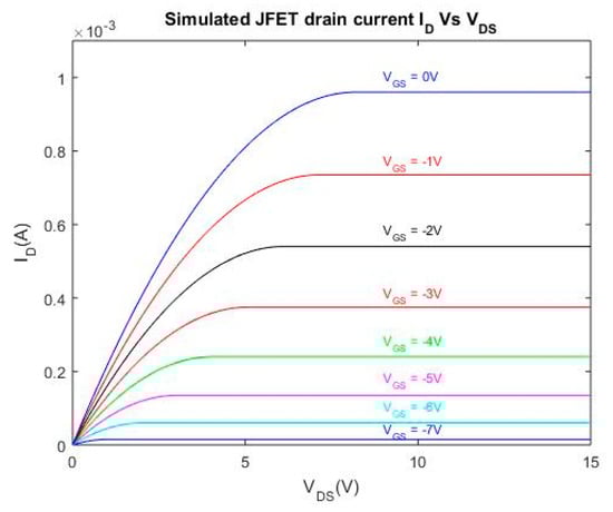
Figure 2.
Simulated junction field effect transistor (JFET) drain characteristics.
The fabricated JFET drain characteristics are shown in Figure 3. Textbook JFET behavior is observed, with ID nearly constant in the saturation region. However, the pinch-off voltage is much larger than the design value, at VGS = −20 V. This could be due to the variation of the doping concentration in the fabrication process or inaccurate doping profiles estimated by SUPREM simulations.
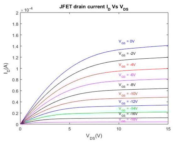
Figure 3.
Drain characteristics of JFET fabricated in the Institute of Microelectronics (IME) process.
We plot the transfer characteristics of JFET at VD = 10 V in Figure 4. The intersection points on the x-axis and y-axis indicate that the pinch-off voltage is −20 V and the saturation drain current IDSS is 0.14 mA at VGS = 0 V, respectively. The actual channel doping level is estimated to be ND = 1.6 × 1017 cm−3, based on the measured Vp using Equation (1), which is a little higher than our proposed doping level of 7 × 1016 cm−3. This dosage variation can be used to explain the difference of predicted and measured pinch-off voltage. Revised SPICE model parameters (see Table 1) were extracted from Figure 3 and Figure 4 in order to support circuit design and simulation. There is a notable difference in the final measurements and target design performance. We believe that this is due to variations in the doping and photolithography steps during the fabrication process. The cut-off frequency is calculated to be 1 GHz according to Equation (2), with the transconductance gm being 1.2 × 10⁻⁵ A/V. The frequency response limitation is dependent on the dimensions and physical constants of the transistors [3]. To obtain a higher frequency response, we can either decrease the channel length L to reduce the capacitance and increase gm, or enhance the channel doping level. In this work, we do not have an option to vary the implant dosage parameters, since these are pre-defined by the fabrication technology. We also have the design limitation of the layout rules with a fixed minimum feature size. However, with possible reductions in feature size by using a more advanced lithography technology, we are confident that the pinch-off voltage and frequency response of the design can be improved for future work.
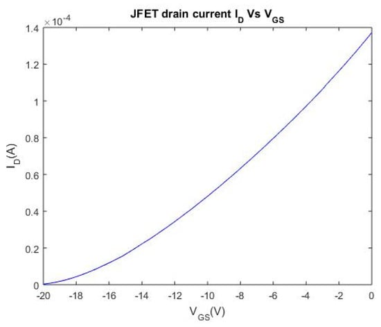
Figure 4.
Transfer characteristics of JFET fabricated in the IME process (VD = 10 V).

Table 1.
JFET HSPICE model parameters.
3. Optoelectronics Integration
In order to demonstrate a full integration of optical components and electronic circuits, we included grating couplers, a strip waveguide, Ge photodiodes, and transimpedance amplifiers in the prototype SOI chip. All optical components are selected from the design library offered by the foundry service. We custom designed the transimpedance amplifiers by using LBJTs and JFETs. Figure 5 shows a block diagram of the integration, using the standard processing parameters supported by A*STAR IME’s silicon photonic multi-project wafer service. A waveguide is used to carry and transmit light on the integrated platform. A 500 nm × 220 nm strip waveguide was used to connect each optical component. The TE 1550-nm surface grating coupler and Ge PIN photodiode were selected in the support library for input/output light coupling and detection. A transimpedance amplifier (TIA) is connected at the back end of the Ge photodetector. As we mentioned previously, the IME silicon photonics general-purpose fabrication process does not support the fabrication of MOS devices due to a lack of polysilicon deposition availability. A MOSFET would also need a high-quality gate oxide. Therefore, we chose to demonstrate the integrated electronic components using an n-channel JFET.
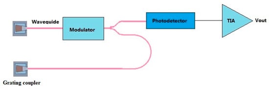
Figure 5.
Block diagram of a complementary metal oxide semiconductor (CMOS) photonic circuit.
Figure 6 shows a microscopic image of the entire integrated circuit. For the optical device, we selected design models from the PDK layout library that have been verified by other research groups. The transimpedance amplifier on the image was constructed by using LBJTs, which was followed by a differential JFET amplifier. The schematic diagram is shown in Figure 7. A photodiode is illustrated by D1; a common-emitter input (Q1) and an emitter follower (Q2) are used to create a low-impedance output and the feedback source in the first stage. A differential JFET amplifier works as the second stage, and provides a regulated output by adjusting the reference voltage VREF. All the resistors were realized by an n-type or p-type implant on the monolithic silicon chip.
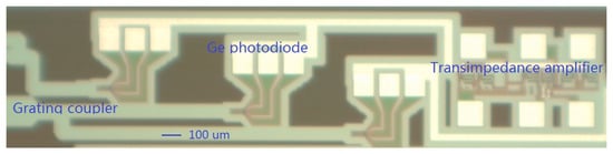
Figure 6.
Microscopic view of the integrated optoelectronic circuit, showing the grating couplers, Ge photodiodes, and transimpedance amplifier fabricated by the IME process.
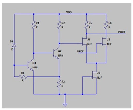
Figure 7.
Transimpedance amplifier constructed by lateral bipolar junction transistors (LBJTs) and JFETs.
Figure 8 shows the optical testing setup, where a tunable laser, Luna Phoniex 1400, and an HP 4145 semiconductor analyzer were used. Successful rectifying characteristics were demonstrated in Figure 9: with an incident light power of 100 µW, the photocurrent of the integrated Ge waveguide photodiode was measured as 10 times higher than the dark current at the 1550-nm wavelength. The photocurrent obtained was intended to be further amplified through the LBJTs and JFETs amplifiers demonstrated in Figure 7.
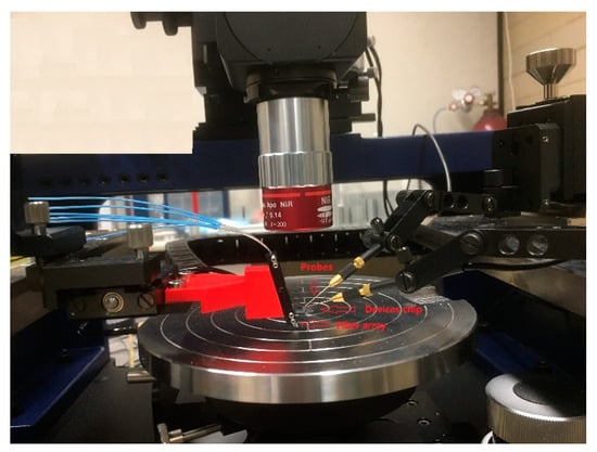
Figure 8.
A setup for Ge photodiode measurement.
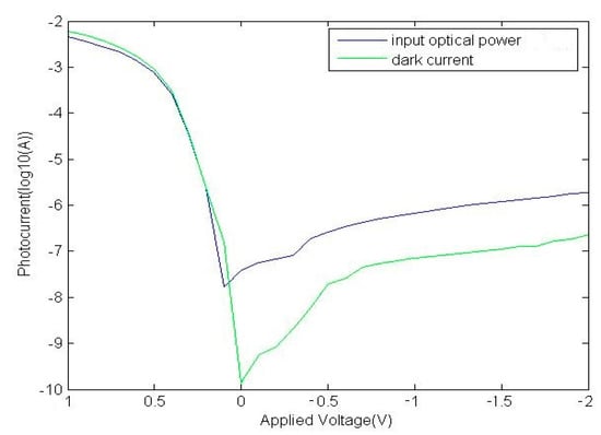
Figure 9.
Measured current–voltage characteristics of the Ge photodiode under 1550-nm optical power (100 µW) and dark condition.
The fabricated JFET behaves well, including the expected drain characteristics (see Figure 3) and transfer characteristics (see Figure 4), with an estimated 1 GHz cut-off frequency. With the revised SPICE model parameters in Table 1, electronic circuitry could be designed and monolithically integrated with the photonic components provided by the IME technology [10,13].
4. Conclusions
We have demonstrated the monolithic integration of photonics and electronics components using a commercial foundry SOI photonics technology provided by Singapore’s A*STAR Institute of Microelectronics (IME). In particular, we have investigated the realization of JFETs integrated with standard optical components. Using available implant parameters and Si film thicknesses, doping levels in the film were estimated and used to design our JFETs. The dimensions were designed in accordance with the technology’s layout rules. Working n-channel JFETs were successfully demonstrated, although the measured pinch-off voltage was much higher than expected. The frequency response of the JFET amplifiers should be adequate for many important applications in SOI-based photonic sensing. With the optimization of the bandwidth, gain, and noise of the transimpedance amplifier, our design could be useful for optical receivers in fiber telecommunications and data centers.
Author Contributions
Conceptualization, S.L. and N.G.T.; methodology, S.L. and N.G.T.; validation, S.L.; formal analysis, S.L., N.G.T., and W.N.Y.; investigation, S.L.; resources, S.L. and W.N.Y.; data curation, S.L. writing—original draft preparation, S.L.; writing—review and editing, N.G.T. and W.N.Y.; visualization, S.L.; supervision, N.G.T. and W.N.Y.; project administration, N.G.T. and W.N.Y.
Funding
This research was funded by National Science and Engineering Research Council of Canada and Canada Research Chairs Program.
Acknowledgments
This project was fabricated by IME with the support of the Silicon Electronic Photonic Integrated Circuits (SiEPIC) workshop program through CMC Microsystems.
Conflicts of Interest
The authors declare no conflict of interest.
References
- Xiong, C.; Gill, D.M.; Proesel, J.E.; Orcutt, J.S.; Haensch, W.; Green, W.M.J. Monolithic 56 Gb/s silicon photonic pulse-amplitude modulation transmitter. Optica 2016, 3, 1060–1065. [Google Scholar] [CrossRef]
- Stojanovic, V.; Ram, R.J.; Popovic, M.; Lin, S.; Moazeni, S.; Wade, M.; Sun, C.; Alloatti, L.; Atabaki, A.; Pavanello, F.; et al. Monolithic silicon-photonic platforms in state-of-the-art CMOS SOI processes. Opt. Express 2018, 26, 13106–13121. [Google Scholar] [CrossRef] [PubMed]
- Kano, K. Semiconductor Devices; Prentice Hall Inc., Simon&Schuster: Upper Saddle River, NJ, USA, 1998. [Google Scholar]
- Safavi-Naeini, M.; Franklin, D.R.; Lerch, M.L.F.; Petasecca, M.; Pignatel, G.U.; Reinhard, M.; Dalla Betta, G.-F.D.; Zorzi, N.; Rosenfeld, A.B. Evaluation of silicon detectors with integrated JFET for biomedical applications. IEEE Trans. Nucl. Sci. 2009, 56, 1051–1055. [Google Scholar] [CrossRef]
- Betta, G.F.D.; Pignatel, G.U.; Verzellesi, G.; Boscardin, M.; Fazzi, A.; Bosisio, L. Monolithic integration of Si-PIN diodes and n-channel double-gate JFET’s for room temperature X-ray spectroscopy. Nucl. Instrum. Methods Phys. Res. A 2001, 458, 275–280. [Google Scholar] [CrossRef]
- Betta, G.-F.D.; Piemonte, C.; Boscardin, M.; Gregori, P.; Zorzi, N.; Fazzi, A.; Pignatel, G.U. An improved PIN photodetector with integrated JFET on high-resistivity silicon. Nucl. Instrum. Methods Phys. Res. A 2006, 567, 368–371. [Google Scholar] [CrossRef]
- Renaud, J.-C.; Nguyen, N.L.; Allovon, M.; Blanconnier, P.; Vuye, S.; Scavennec, A. GaInAs monolithic photoreceiver integrating p-i-n/JFET with diffused junctions and a resistor. J. Lightwave Technol. 1988, 6, 1507–1511. [Google Scholar] [CrossRef]
- Wang, J.; Yu, M.-B.; Lo, G.-Q.; Kwong, D.-L.; Lee, S. Silicon waveguide integrated Germanium JFET photodetector with improved speed performance. IEEE Photonics Technol. Lett. 2011, 23, 765–767. [Google Scholar] [CrossRef]
- Liow, T.-Y.; Ang, K.-W.; Fang, Q.; Song, J.-F.; Xiong, Y.-Z.; Yu, M.-B.; Lo, G.-Q.; Kwong, D.-L. Silicon modulators and Germanium photodetectors on SOI: Monolithic integration, compatibility, and performance optimization. IEEE J. Sel. Top. Quantum Electron. 2010, 16, 307–315. [Google Scholar] [CrossRef]
- Li, S.-X.; Tarr, N.G.; Ye, W.N. Monolithic integration of SOI waveguide photodetectors and transimpedance amplifiers. Int. Soc. Opt. Photonics 2018, 10537, 105371M. [Google Scholar]
- Sima, D. Principles of Semiconductor Devices, 2nd ed.; Oxford University Press: Oxford, UK, 2012. [Google Scholar]
- Colinge, J.-P.; Colinge, C.A. Physics of Semiconductor Devices; Kluwer Academic Publishers: Boston, MA, USA, 2002. [Google Scholar]
- Li, S.-X.; Tarr, N.G.; Ye, W.N. Monolithic integration of Opto-electronics by silicon photonics foundry service. Proc. SPIE OPTO 2019, 10922, 1092217. [Google Scholar]
© 2019 by the authors. Licensee MDPI, Basel, Switzerland. This article is an open access article distributed under the terms and conditions of the Creative Commons Attribution (CC BY) license (http://creativecommons.org/licenses/by/4.0/).