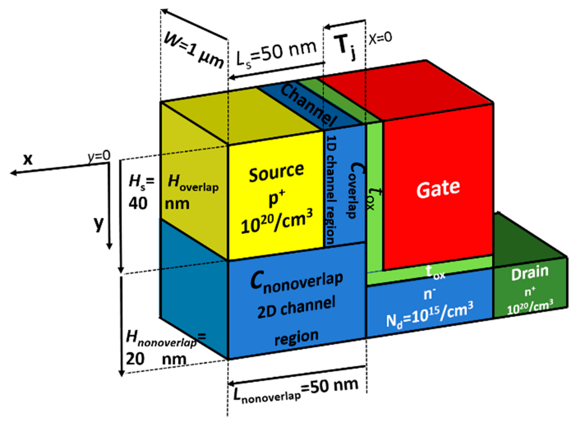
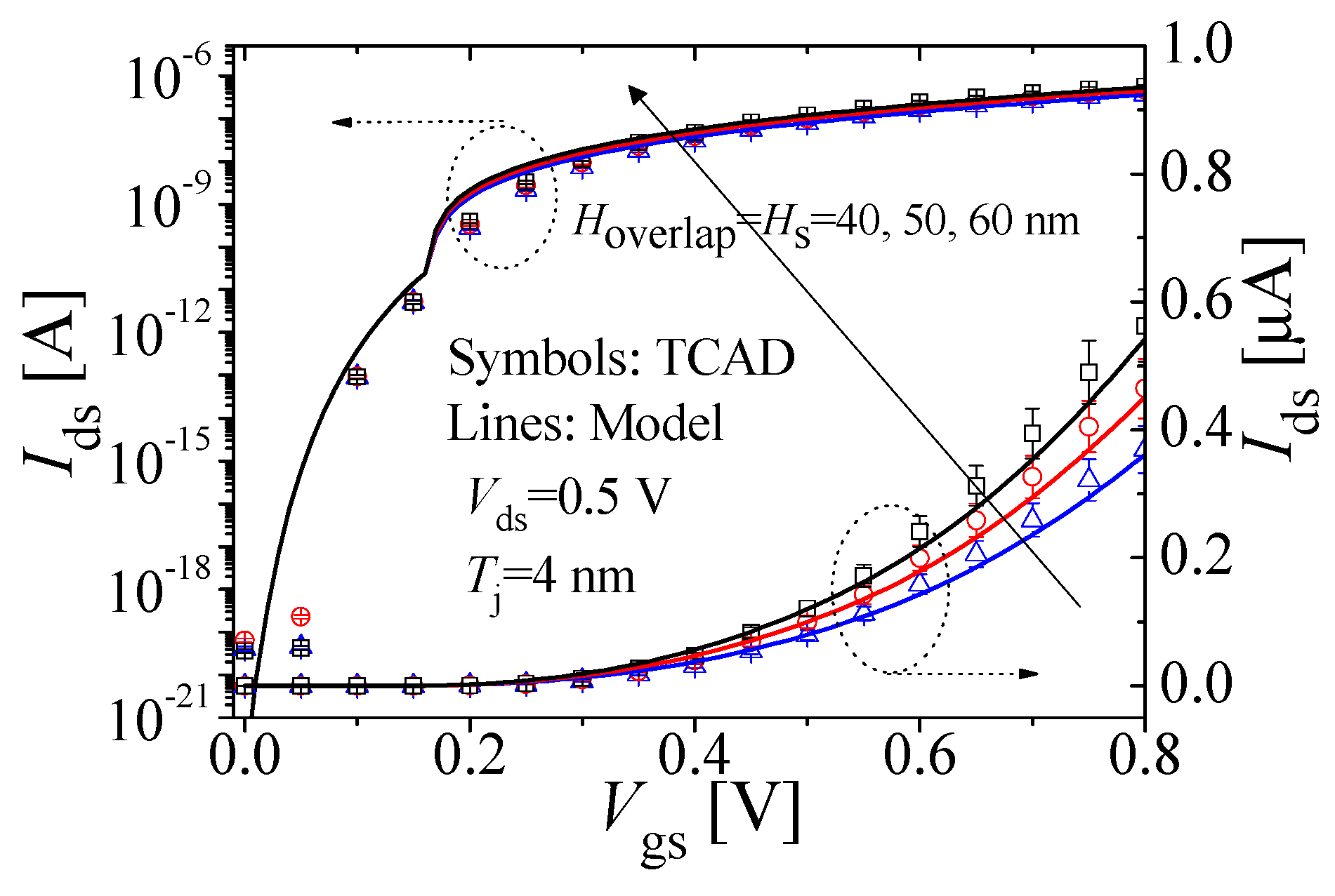
Figure 1 shows the schematic of the LTFET. The channel region shown in blue color is found in an L-shape and is sandwiched between the gate and the source. The part of the channel region found in between the source and gate regions is termed as
Coverlap with height (
Hoverlap) = 40 nm and length (
Tj) = 4 nm. The source and drain are p
+ (
Na = 10
20 cm
−3) and n
+ (
Ndrain = 10
20 cm
−3) doped, respectively, while the channel is lightly n
− doped (
Nd = 10
15 cm
−3). The source region height (
Hs) and length (
Ls) are 40 and 50 nm, respectively. The bottom part of the channel, which is not in between the source and gate regions, is termed as
Cnonoverlap and has a height (
Hnonoverlap) = 20 nm, and length (
Lnonoverlap) = 50 nm. An HfO
2 dielectric of thickness (
tox) = 2 nm for gate oxide was considered.
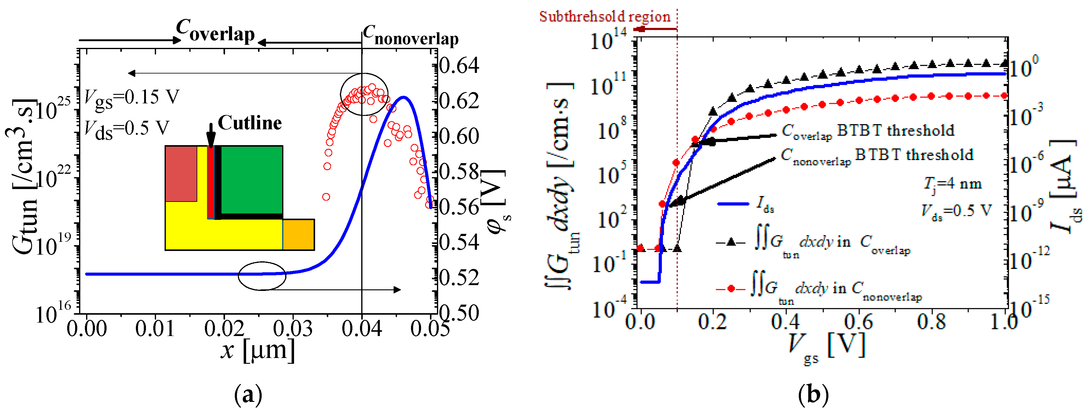
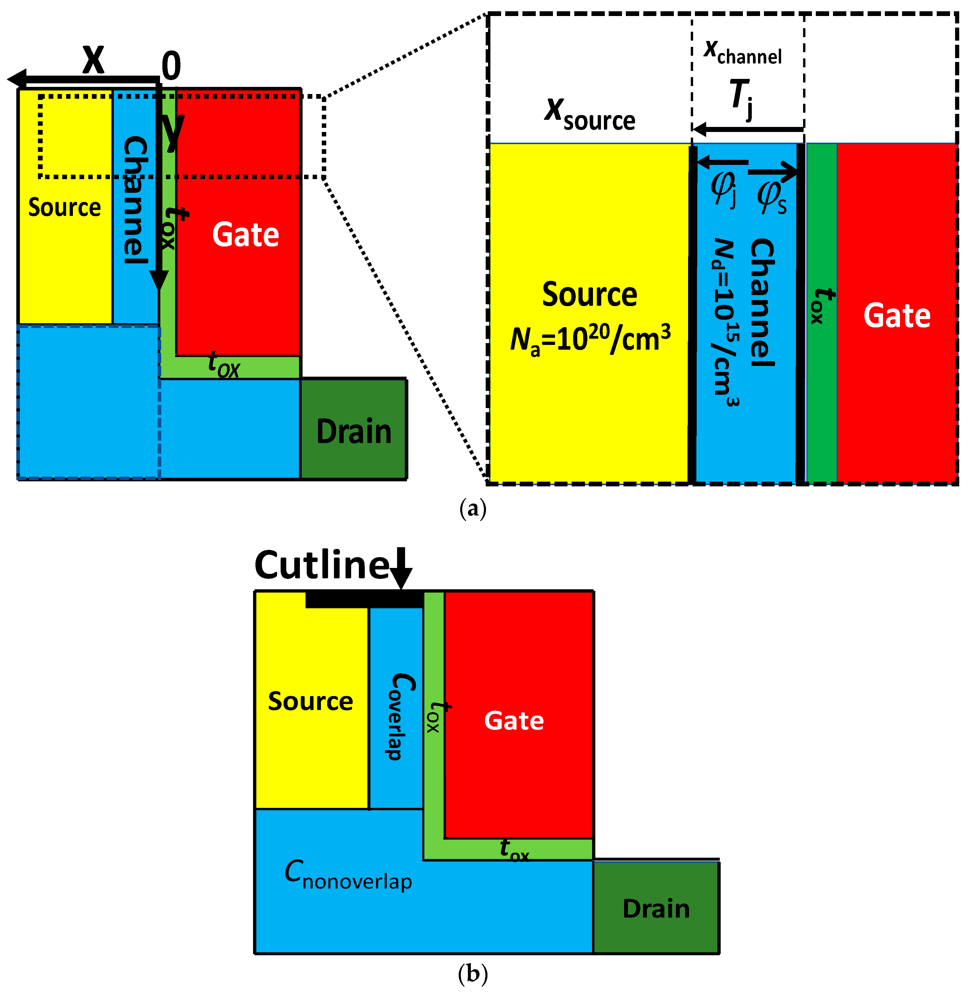
As shown in
Figure 1, the source has a sharp corner marked by an X in
Figure 1. The electric field from the gate converges at and around this sharp source corner, increasing the potential around this point. The right axis in
Figure 2a shows surface potential (
φs) at
Vgs = 0.15 V and
Vds = 0.5 V. As shown in
Figure 2a,
φs sharply rises in
Cnonoverlap because of convergence of the electric field, whereas
φs is less in
Coverlap where this convergence does not take place. This convergence affects the BTBT threshold voltage of
Coverlap and
Cnonoverlap.
Cnonoverlap is found to have a lower BTBT threshold voltage because of this increased
φs. Meanwhile,
Coverlap has a significantly higher BTBT threshold voltage because of the lower potential [
10]. This can be seen in
Figure 2b, which shows integrated BTBT tunneling rates [
10] (
Gtuns) in
x and
y directions in
Coverlap and
Cnonoverlap, respectively; that is,
in
Coverlap (black triangles) and
in
Cnonoverlap (red circles) in the left axis.
Figure 2b clearly shows that
Cnonoverlap turns on earlier than
Coverlap. The right axis in
Figure 2b shows the drain-source current (
Ids) as a function of gate–source bias (
Vgs) of LTFET. It is shown that in the subthreshold part of the
Ids–
Vgs characteristics, only the
Cnonoverlap is active.
Coverlap turns on at
Vgs = 0.15 V. When
Coverlap turns on, its
Gtun is significantly higher because of 1D BTBT paths. As a result, it dominates the 2D
Gtun in
Cnonoverlap, as can be seen in
Figure 2b. Based on this analysis,
Ids–
Vgs characteristics of LTFET were modeled in two parts, first the 2D model in
Cnonoverlap for the subthreshold region and then the 1D model in
Coverlap.
2.1. 2D Model: Cnonoverlap Model
The 2D model is based on the work in [
3]. The following assumptions are used in this model: (1) Electric fields are assumed to be completely circular and terminate from gate to source. This helps in obtaining a convenient expression for the tunneling length (
Wt); (2) Gate dielectric is treated as the same material as the channel with an equivalent dielectric thickness
t’
ox given by
t’
ox =
toxεsi/
εox, where
tox,
εsi, and
εox are the physical dielectric thickness, silicon dielectric permittivity, and oxide dielectric permittivity, respectively. This is necessary to ensure a continuous and perfectly circular electric field from the gate-to-channel/gate dielectric interface, and finally terminate at the source. Without this assumption, the electric field will be discontinuous, that is, not perfectly circular in its path from gate to source. In this work,
Wt is conveniently calculated as the length along the perfectly circular electric field arc, from gate to source, as will be shown below. If a discontinuity arises in the circularity of the electric field arc, such convenient calculation of W
t will not be possible; (3) The source is assumed to be completely depleted, and depletion length is ignored. The source is heavily doped. Depletion length is inversely proportional to doping concentration [
3]. This makes the source depletion length negligible. Including the source depletion length would add complexity to the model without significantly increasing the accuracy of the model; (4) The source is assumed to be touching the gate.
Table 1 mentions most of the symbols used in the equations below.
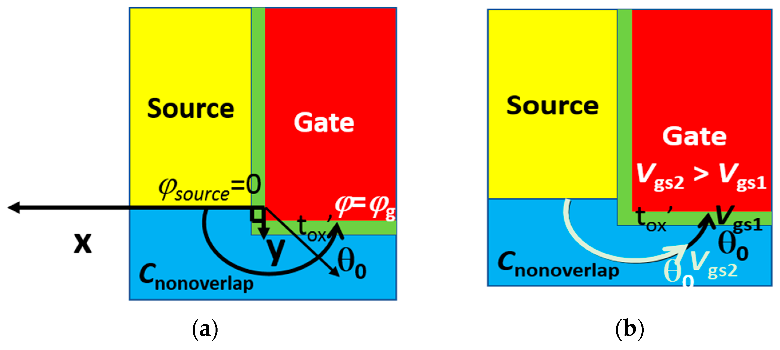
With these assumptions, the boundary conditions at source and gate can be given by
where
φsource is assumed to be 0 V and
φg is the gate–source bias minus the flat band voltage (
Vfb), that is,
φg =
Vgs −
Vfb. The solution of potential in polar co-ordinates is given by
The above boundary condition along with
θ0 is shown in
Figure 3a. Thanks to assumptions 1 and 2,
Wt is calculated as the length along a perfectly circular electric field line as follows:
where
θ0 is given by
θ0 =
πEg/(2
qφg), (where
Eg is the bandgap, and
q is the charge on an electron) and is the angle when the potential difference between the source edge and some point along the electric field line becomes equal to
Eg/
q.
θ0 is obtained by substituting the BTBT condition, that is,
φ =
Eg/
q in (2), and inverting it. Since
θ0 is bias-dependent,
θ0 decreases, and
Wt decreases as
Vgs bias increases. This is illustrated in
Figure 3b.
r0 is the radius of the electric field arc and is given by
r0 =
t’
ox/
cos (
θ0). Drain current expression in
Cnonoverlap (
Ids_Cnonoverlap) is given by the following equation for
D = 2.5 [
3]:
where
W (=10
−4 cm) is the device width, and
Ak = 1 × 10
15 eV
0.5·cm
−1/2·s
−1·V
−2.5 and
Bk = 1.5 × 10
7 V·cm
−1·eV
−1.5 are the parameters used in the dynamic nonlocal BTBT model. There is one notable difference between this work and [
3] which is that, as
Coverlap turns on,
Ids_Cnonoverlap is assumed to saturate. This is in line with the results presented in
Figure 2b. Once
Coverlap turns on, it dominates, and
Cnonoverlap does not have any significant contribution beyond that point. Without this assumption, the model overestimates
Ids_Cnonoverlap in the high
Vgs region.
2.2. 1D Model: Coverlap Model
Figure 4a shows a magnified
Coverlap and source regions. The channel region considered in the 1D model comprises the
Coverlap region.
Figure 4a mentions the important parameters used in the 1D model, including the location of
φs and junction potential (
φj).
φj is the potential at the junction of the source and channel region in
Figure 4a. The device origin is at the top of the channel/gate dielectric interface, and
xchannel and
xsource correspond to the
x-coordinate in channel and source regions, respectively. The dimension for the 1D model is along the
x-direction, as shown by the cutline shown in
Figure 4b. The cutline begins at the channel/gate dielectric interface and ends in the source region.
Figure 5d–f and
Figure 6a,b are along the black cutline shown in
Figure 4b.
The 1D model is based on the solution of the 1D Poisson equation. Integrating the 1D Poisson equation once, in source and channel regions, and neglecting electron and hole carrier concentrations yields the electric field in the respective regions, which are given by
where
Ldep is the depletion length of the source region. Integrating (5) and (6) again yields potential in source and channel regions, which is given by
where
Cox is the gate oxide capacitance,
φdep is the source depletion potential, and γ = (2
εsiqNa)
1/2/
Cox. With the potential profile known,
Wt can be calculated. Because (9) is derived from the depletion approximation, the smoothing function from [
11,
12,
13] was used to model strong inversion of the electron.
There are two different 1D BTBT mechanisms present in LTFET [
8]. One is the source-to-channel BTBT, which starts at low bias, and the other is the channel-to-channel BTBT, which takes place at high
Vgs bias. The first source to channel the 1D BTBT model is discussed.
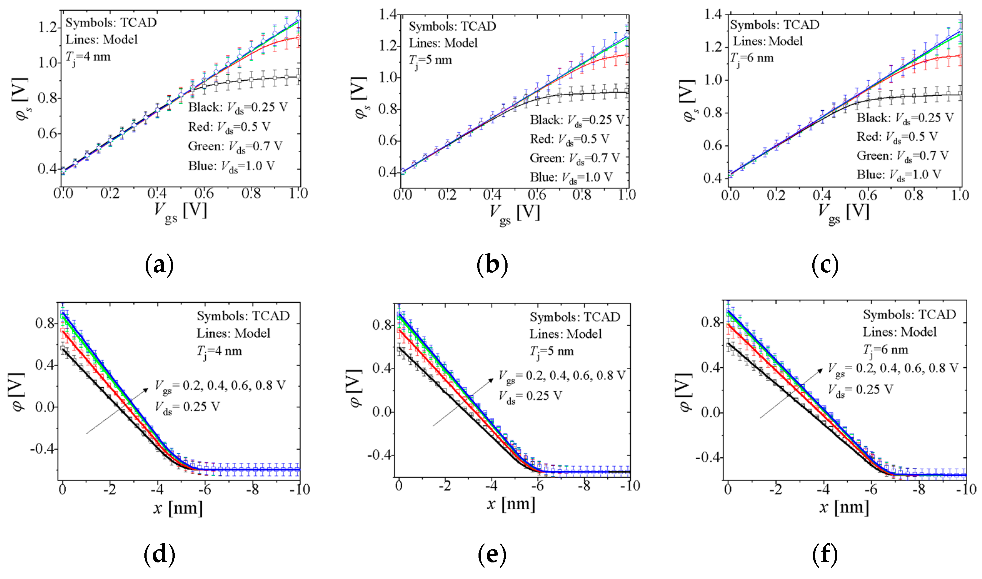
The potential profile within the channel is assumed to be linear, as seen in
Figure 5d–f, which is given by
where
m is the slope of the linear potential profile in the channel,
m = (
φs −
φj)/
Tj.
φj can be found from (8) by using
xchannel =
Tj.
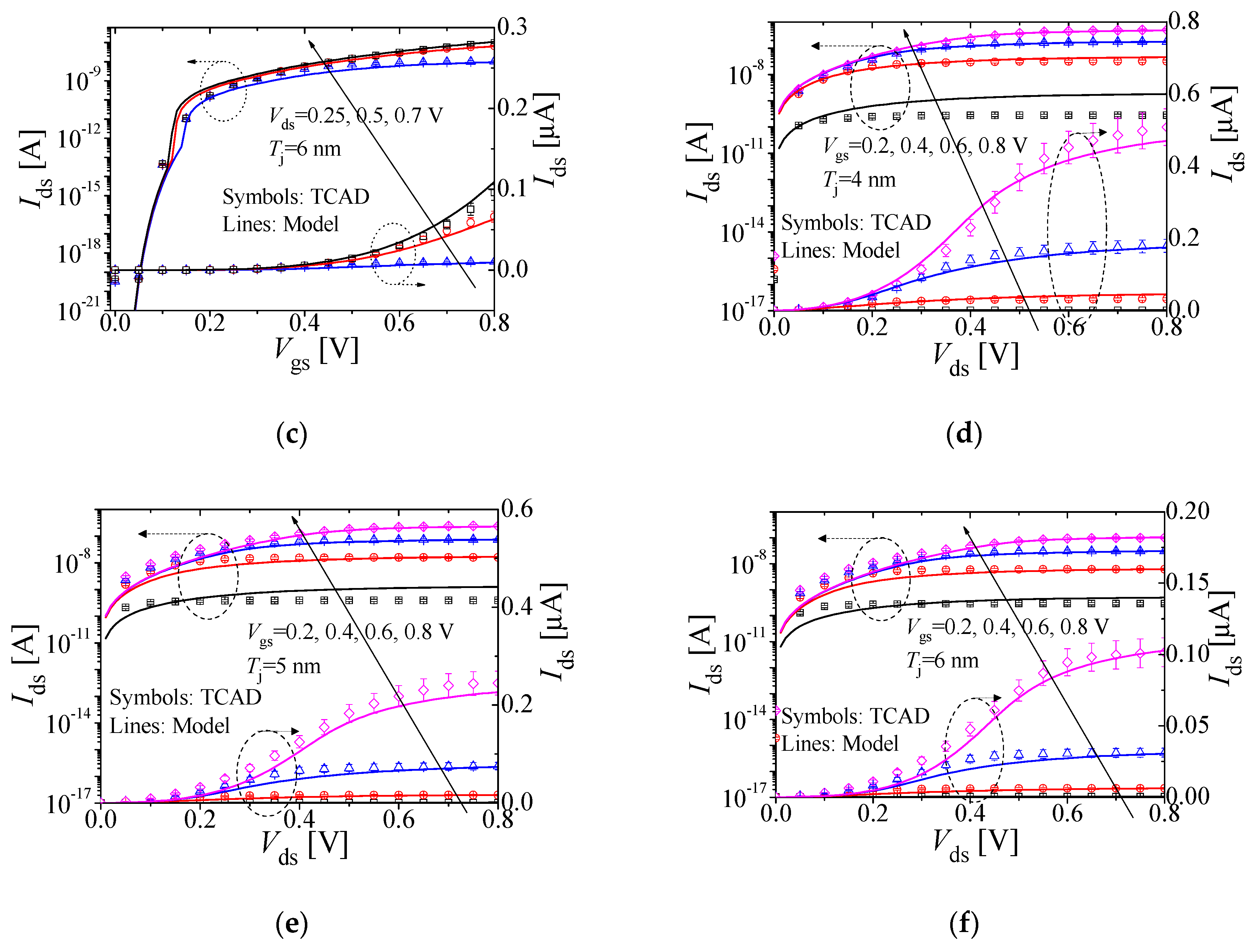
Figure 5a–c shows
φs as a function of
Vgs of LTFET with
Tj = 4, 5, and 6 nm at different
Vds biases, respectively.
Figure 5d–f shows the potential profile along the cutline shown in
Figure 4b for LTFET with
Tj = 4, 5, and 6 nm at different
Vgs and
Vds = 0.25 V, respectively. Symbols and lines denote the simulation results of TCAD and the proposed potential model, respectively. Reasonable agreement is observed within a maximum error of 10% between the model and TCAD simulations.
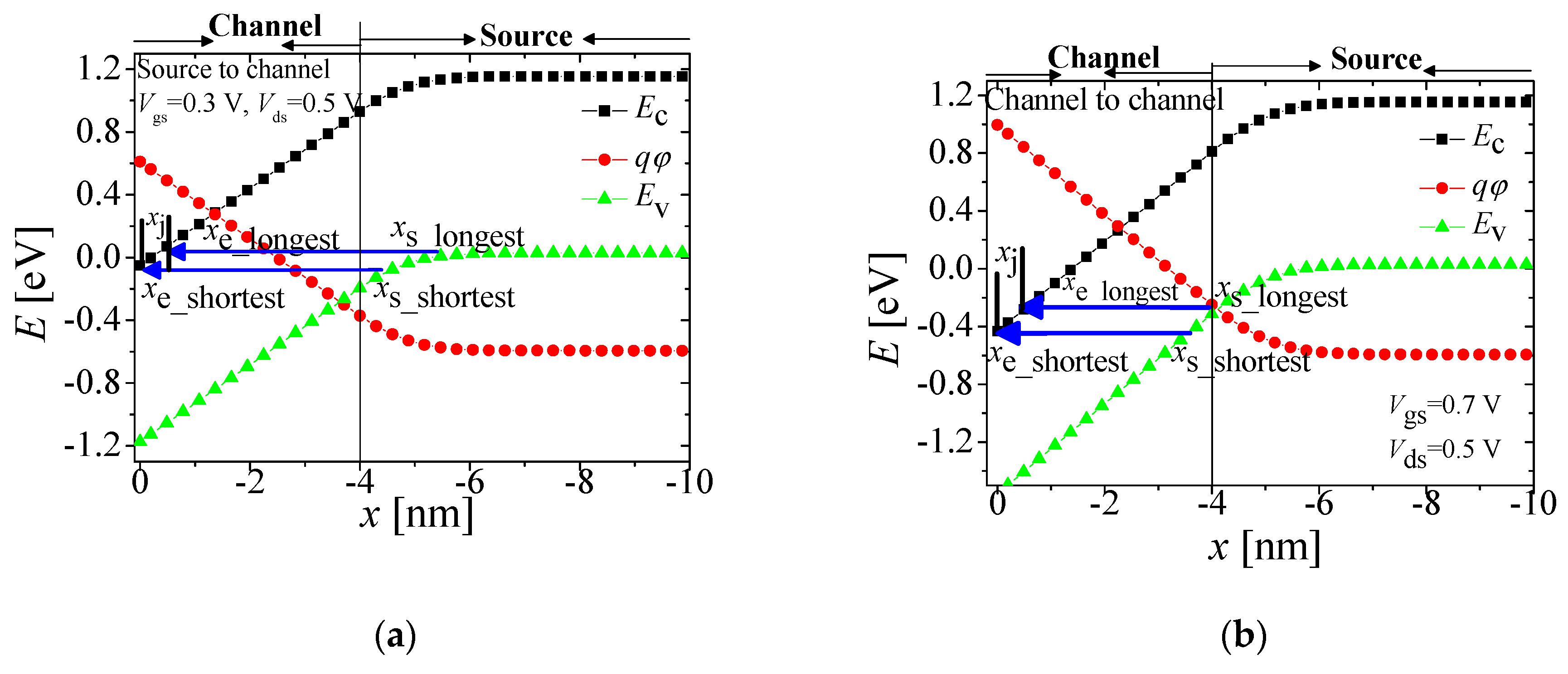
Figure 6a shows a band diagram at
Vgs = 0.3 V and
Vds = 0.5 V, along the cutline of
Figure 4b. Black and green symbols represent conduction band minimum energy (
Ec) and valence band maximum energy (
Ev), respectively. Red circles represent potential. Arrows denote
Wts. The longest
Wt (
Wt_longest) originates where
φsource =
φdep, and the shortest
Wt (
Wt_shortest) originates from where the potential is the highest, that is,
φs. The starting and ending points for
Wt_shortest are
xs_shortest and
xe_shortest, respectively, and the starting and ending points for
Wt_longest are
xs_longest and
xe_longest, respectively, which are all indicated by arrows in
Figure 6a.
xs_longest naturally starts from
Ldep, that is,
xs_longest = −
abs(
Ldep +
Tj), and the ending point for the
Wt_shortest is the surface, that is,
xe_shortest = 0.
xe_longest is the point where the BTBT condition for
Wt_longest, that is,
φ(
xe_longest) =
φdep +
Eg/
q, is satisfied. By substituting this BTBT condition in (10) and inverting it,
xe_longest is given by
xe_longest = (
φdep +
Eg/
q −
φs)T
j/(
φs −
φj).
xs_shortest is the point where the BTBT condition for
Wt_shortest, that is,
φ(
xs_shortest) =
φs −
Eg/
q, is satisfied. By substituting this BTBT condition in (7) and inverting it,
xs_shortest is given by
Finally,
Wt_shortest and
Wt_longest are given by
Gtun is given by Kane’s model [
14]
Ids for source-to-channel BTBT (
Ids_s_c) is given by
where
xj is the integration limit indicated in
Figure 6a, and is equal to
. In (14), a constant average
Gtun, that is,
, is used. Here,
Gtun_shortest and
Gtun_longest are found by using
Wt =
Wt_shortest and
Wt_longest in (13), respectively.
Gtun is a function of
Wt, as can be inferred from (13). The integral in (14), however, is with respect to
x. Finding a closed-form expression for
Ids_s_c then necessitates expressing
Wt as a function of
x. However, because
Wt cannot be expressed as a function of
x,
Wt can only be found for fixed BTBT boundary conditions, as done in (12a, b). In this scenario,
dWt/
dx cannot be evaluated. As a result, there is no closed-form expression available for
Gtun integrated as a function of
x. Therefore, the simplification of using average
Gtun was necessary and, as it will be shown in
Section 3, the average
Gtun approximates the integral of
Gtun with respect to
x reasonably well. When the bias is high enough, the potential increases so much that BTBT becomes possible from even inside the channel. This is illustrated by the band diagram shown in
Figure 6b along the cutline of
Figure 4b. Here,
Ev/
Ec becomes aligned within the channel, as illustrated by the arrows, in addition to the source/channel
Ev/
Ec alignment. Here,
Wt_longest starts from
xs_longest =
Tj and ends at
xe_longest, where the BTBT condition,
φ(
xe_longest) =
φj +
Eg/
q, is satisfied. Similarly,
Wt_shortest starts at
xs_shortest, where the BTBT condition,
φ(
xs_shortest) =
φs −
Eg/
q, is satisfied and ends at
xe_shortest = 0. By substituting these boundary conditions in (10) and inverting it,
xe_longest and
xs_shortest can be calculated as
xe_longest = (
φj +
Eg/
q −
φs)
Tj/(
φs −
φj) and
xs_shortest = −
EgTj/(
q(
φs −
φj)). As can be seen in
Figure 6b,
Wt is almost constant within the channel. Therefore, in the channel-to-channel regime,
Gtun_shortest ≈
Gtun(
Wt_longest) ≈
Gtun(
Wt_shortest). This means that
Gtun(
x) can be taken out of the integral in the channel-to-channel drain current (
Ids_c_c) expression, which is given by
The total
Ids is given by


