1. Introduction
Sapphire has many special characteristics such as high hardness, great thermal stability, good light transmission, excellent electrical insulation and chemical inertness [
1]. It is widely used in mechanics, optics, electronics, light emitting diodes (LEDs) industry and other fields [
2]. In recent years, LEDs have attracted great attention due to their environmental friendliness, longer life span and high energy efficiency while comparing to traditional lighting sources [
3]. In LED manufacturing processes, sapphire is the predominant material used as substrates for gallium and indium nitride films [
4]. The surface of sapphire is known to play a critical role in determining the crystal quality of the grown GaN epilayer by metal–organic chemical vapor deposition (MOCVD) [
5,
6]. When growing thin film on sapphire substrates with a poor surface quality, the film tends to grow preferentially in scratches. The morphology and size of the scratch will be completely reproduced on the film surface, which will lead to poor connections between thin film layers. Therefore, surface quality is an important parameter that influences the performance of the devices.
Chemical mechanical polishing (CMP) has been widely and effectively applied to a variety of materials in the last two decades, including semiconductors wafers, crystals, glasses, special metals, plastics and computer disks [
7,
8]. CMP is becoming popular due to its advantages over other surface finishing techniques, advantages such as little or no surface and subsurface damages, and elimination of surface defects [
9,
10,
11]. Sapphire is no exception. CMP is normally used as the last processing step for sapphire substrate polishing. However, sapphire substrates are noted for their physical properties of wear and corrosion resistance, and in many cases the efficiency of CMP processes are low [
12]. Fine surface machining and polishing of sapphire substrates may exceed 80% of the total production cost. In CMP processing, the polishing slurry distribution on the sapphire surface is uneven and the slurry tends to quickly leave the processing area due to the centrifugal force, resulting in uneven surface and polishing slurry waste. Statistics [
13] show that in the process of mass processing of sapphire substrates, the proportion of rupture and edge collapse is high, accounting for 6% of all yield losses, and the surface of the polished sapphire substrates have slight scratches. Therefore, developing a highly efficient and high precision sapphire substrate polishing method has become extremely urgent.
Dielectrophoresis (DEP) has been proven to manipulate micro particles [
14], and successfully applied in many fields. Zhu used DEP to trap and separate yeast cells from a mixed suspension with PS microspheres and achieved a high capture rate and separation efficiency [
15]. Das demonstrated the design, fabrication and testing of a label-free continuous manipulation and separation micro-device of particles/biological cells suspended on a medium based on conventional DEP [
16]. Zhang indirectly removed heavy metal ions in water by using DEP to control and separate rare earth oxides [
17]. Nastruzzi studied applications of DEP-based lab-on-a-chip devices in pharmaceutical sciences and biomedicine [
18]. Shearer used DEP to fabricate atomic force microscope probes [
19].
In this study, the authors apply a non-uniform electric field to produce a DEP effect on polishing slurry consisting of abrasive particles in the polishing area of the traditional polishing machine. Under DEP force, slurry was compelled to stay with the polishing pad for a longer time to improve the distribution of slurry between the polishing pad and the sapphire substrate [
20]. The principle of dielectrophoresis polishing (DEPP) will be explained and a set of experiments for comparison will be carried out. Finally, the summary of this study will be presented.
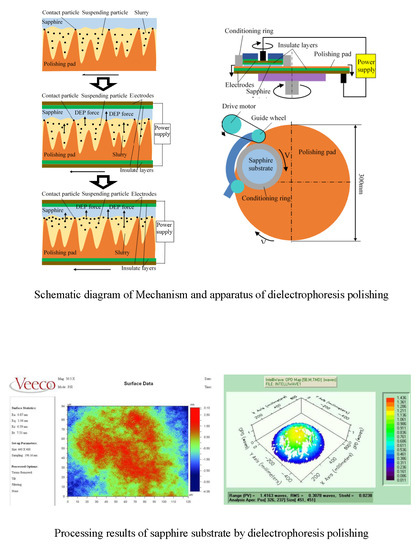
2. Dielectrophoresis Polishing and Apparatus
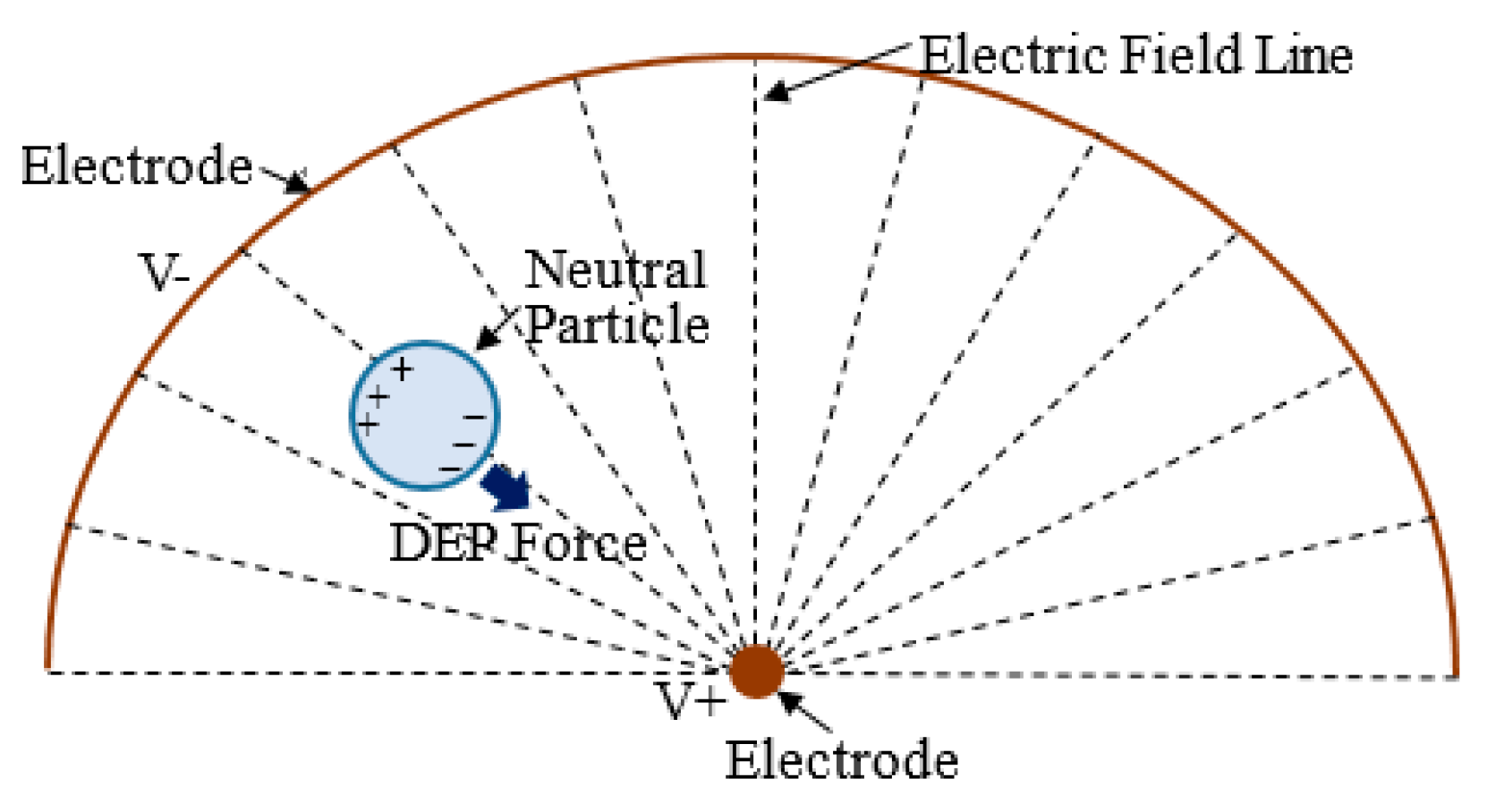
DEP is a physical phenomenon in which electrically neutral particles in a non-uniform electric field is subjected to an electric field force [
21]. The existence of the force does not require the object being electrically charged, and the direction of the force points towards the electrode. This force is called the DEP force, and
Figure 1 shows an electrically neutral particle in a non-uniform electric field. All neutral particles have the DEP effect in non-uniform electric fields, where the value of the DEP force depends on the electrical property, size and shape of the particles, and the change rate of the electric field intensity. The DEPP method utilizes the DEP effect of abrasives in a non-uniform electric field to assist polishing.
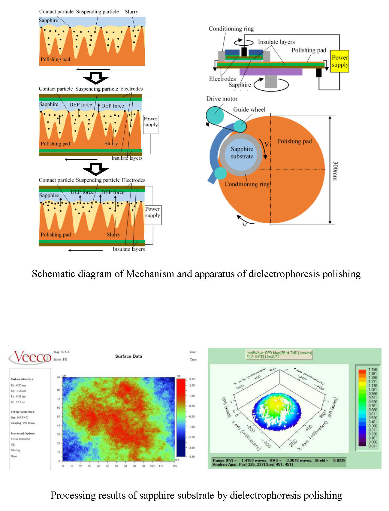
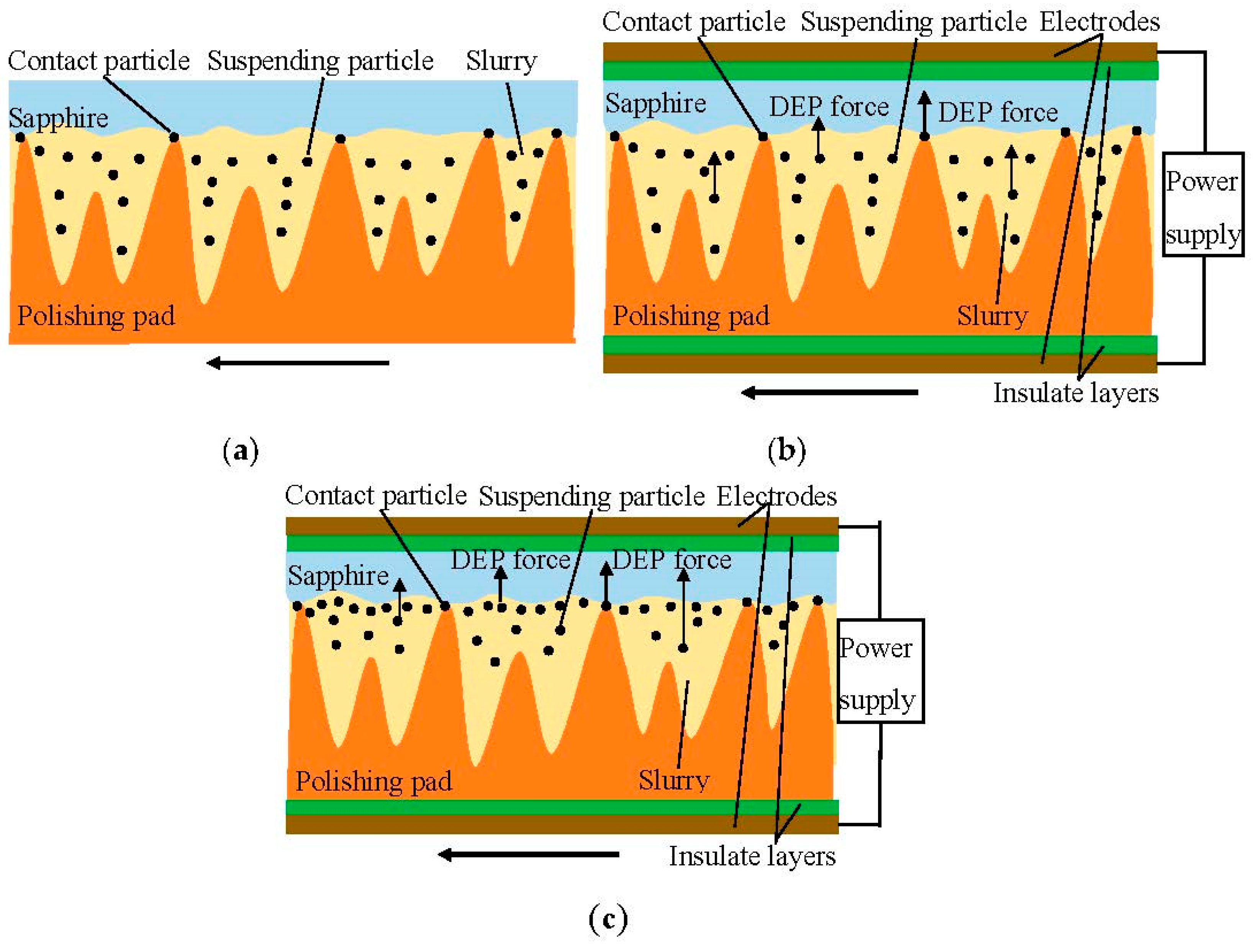
The mechanism of DEPP is shown in
Figure 2. The workpiece is a sapphire substrate, and its surface has a certain degree of surface roughness after grinding. When the polishing area does not form a non-uniform electric field (traditional CMP), abrasives will be randomly suspended in the polishing slurry, and only a small amount of abrasives will be brought in contact with the sapphire substrate and polishing pad that generate effective material removal, as shown in
Figure 2a. The insulating layer and the electrode are added in the vertical direction of the polishing area to form a non-uniform electric field, and the abrasives are polarized subject to DEP force, as shown in
Figure 2b. Under DEP force, the abrasives will move in the direction towards the electrode and congregate on the surface of the sapphire substrate to effectively increase the contact with the sapphire substrate and the polishing pad. In the same time, polishing slurry that follows the abrasives tends to move towards the sapphire substrate to increase the pressure between the sapphire substrate and polishing slurry, as shown in
Figure 2c. According to
Figure 2, we can see that the DEPP technology can drive the abrasives in polishing slurry to move and assemble on the surface of sapphire substrates, resulting in more abrasives to participate in the polishing process, to improve the material removal and to increase the efficiency of sapphire polishing.
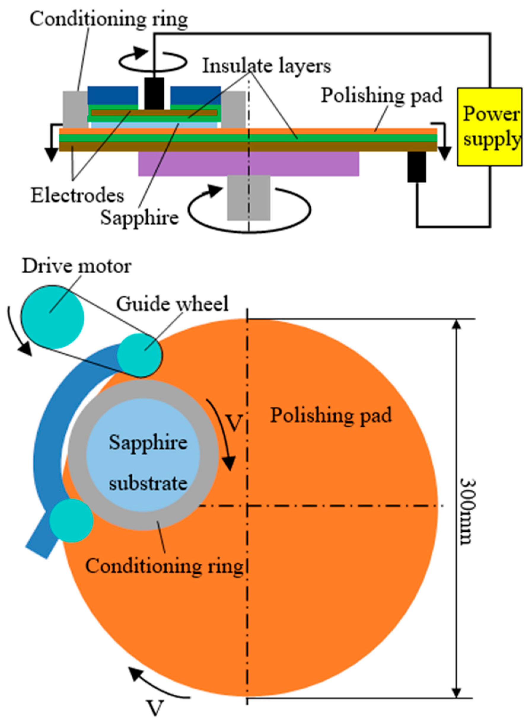
The schematic diagram of the DEPP apparatus is shown in
Figure 3, which is obtained by retrofitting a traditional flat polishing machine. The lower plate is made of an insulating layer, an electrode and a polishing pad. The upper plate is made of an insulating layer and an electrode, and a sapphire substrate as the workpiece with paraffin is pasted on the upper plate. The sapphire substrate and the lower plate are driven by two different motors, and the rotating speed of the motors can be adjusted independently. A high voltage power supply connects the electrodes through carbon brushes on the plates, forming a non-uniform electric field for the DEPP machine.
3. Simulation Analysis
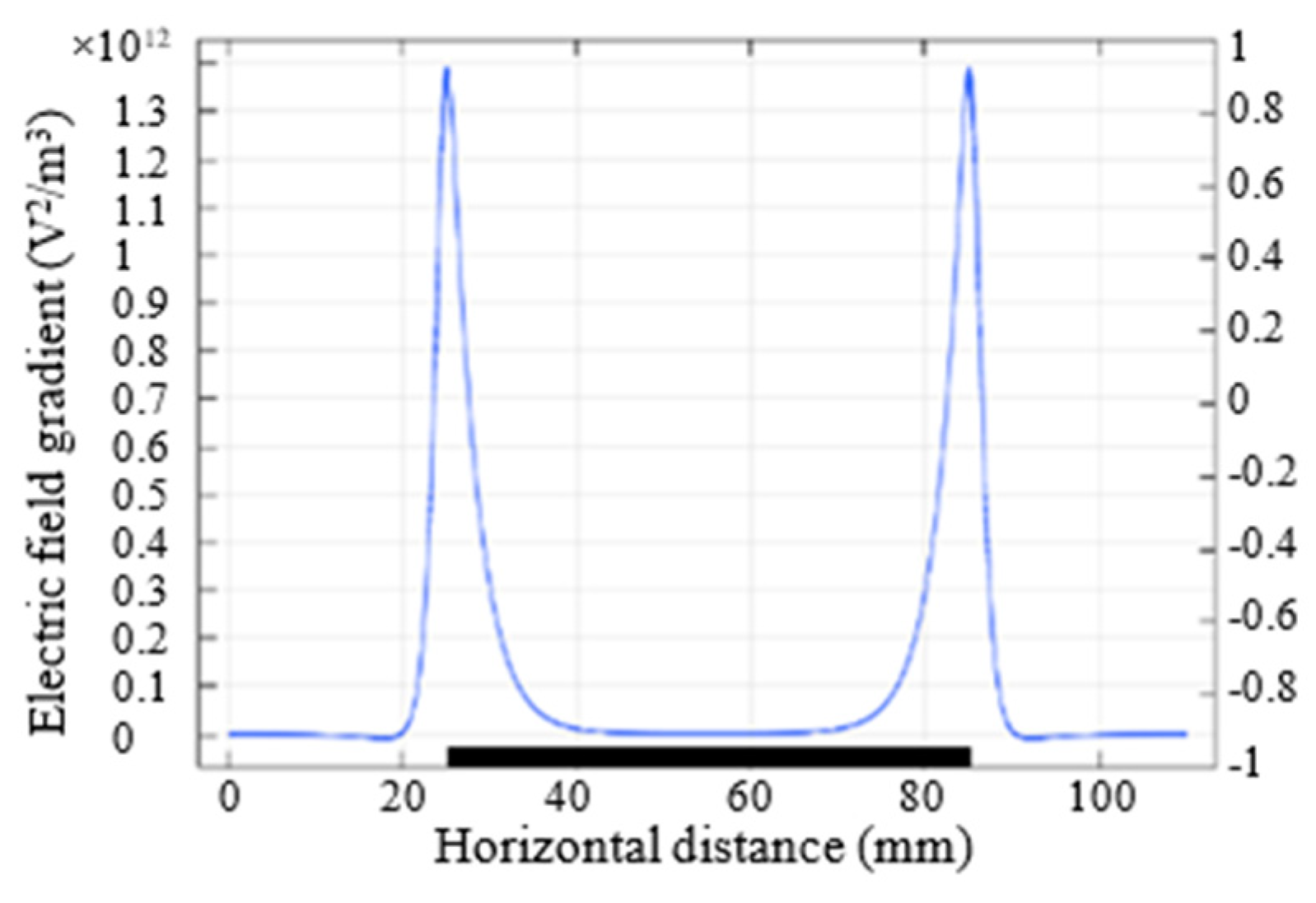
According to the designed electrodes, COMSOL software was used to simulate the electric field gradient, DEP force and resultant force (DEP force and centripetal force combinedly act on abrasive). The diameter of the upper electrode was set as 60 mm, the electric field intensity was 300 V/mm and the frequency was 40 Hz.
Figure 4 shows the simulation of the electric field gradient. It can be seen that the electric field gradient increases gradually from the center to the edge of the upper electrode, so the DEP force in the electric field increases gradually from the center to the edge of the upper electrode. Because the electrodes were axisymmetric, only the symmetrical parts were simulated.
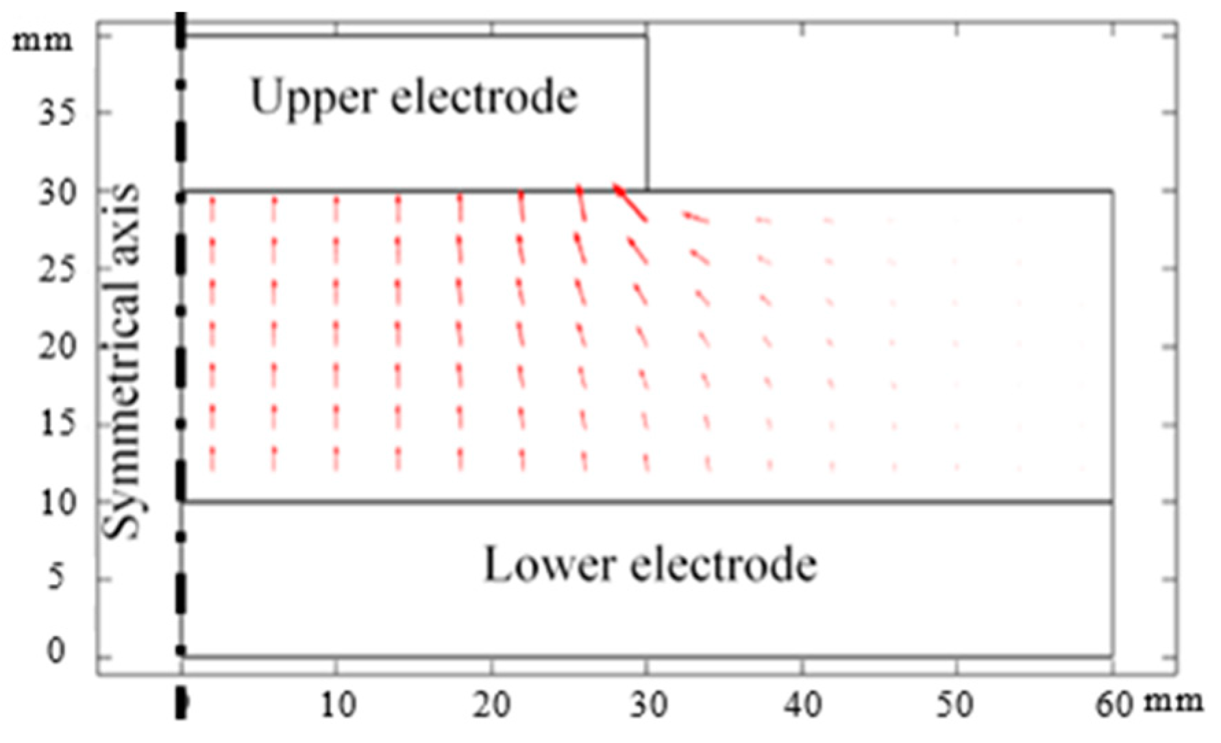
Figure 5 shows the magnitude and direction of DEP force on the abrasive between the upper and lower electrodes. It can be concluded that the abrasive between the electrodes will be subject to DEP force in an approximately vertical direction, and at the edge of the upper electrode, the DEP force is the largest, which is consistent with the simulation results of the electric field gradient.
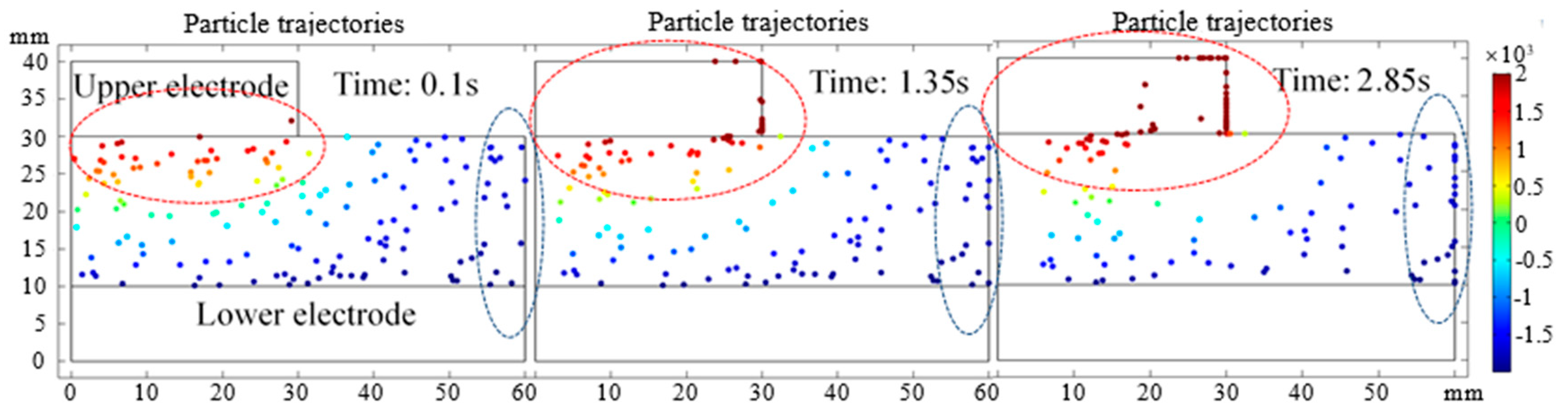
The movement of the SiO
2 abrasive under both DEP force and centrifugal force was simulated. As shown in
Figure 6, 0.1 s was the initial state of the SiO
2 abrasive. At 1.35 s, some of the abrasive were aggregated on the lower surface of upper electrode by DEP force, and at the same time some were moved to the right by centrifugal force. At 2.85 s, more abrasive gathered on the lower surface of the upper electrode, and some abrasive were thrown out of the electric field area. At 1.35 s and 2.85 s, due to the larger DEP force at the edge of the upper electrode, much abrasive gathered on the edge and the upper surface of upper electrode. This phenomenon will not occur in actual processing, because the workpiece is located below the electrode, and the diameter of the workpiece is larger than that of the upper electrode, so the abrasive will only gather on the surface of the workpiece.
The simulation results show that the abrasive can still move towards the surface of the workpiece when it is subjected to both DEP force and centrifugal force, which indicates that the idea of using the DEP effect of abrasive to assist polishing is feasible.
4. Experimental Procedures
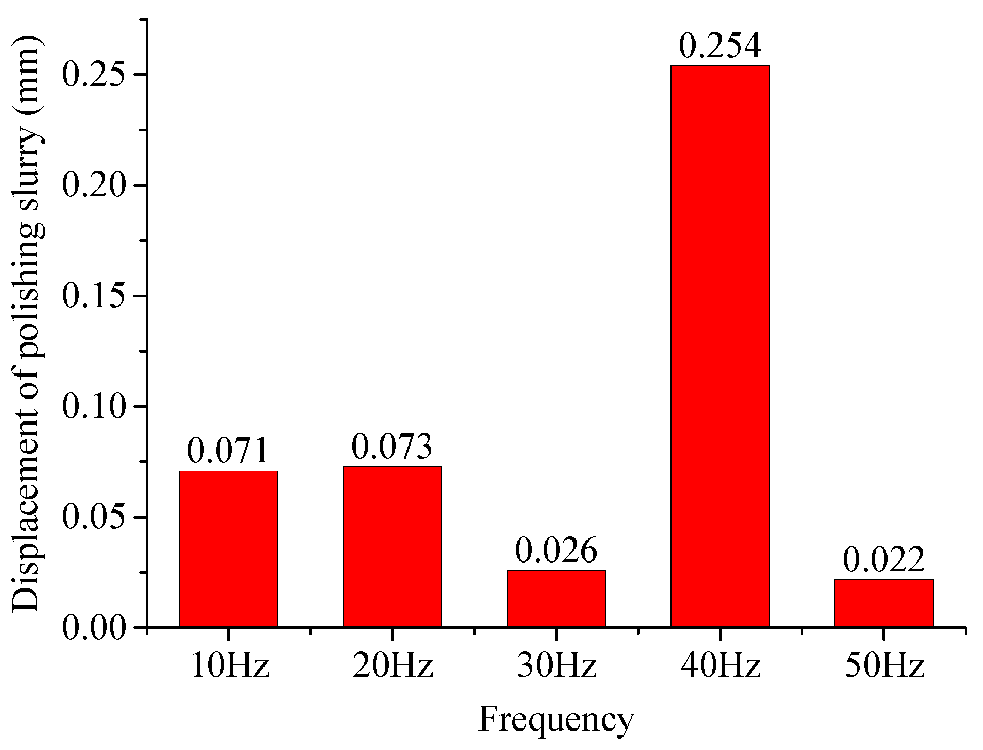
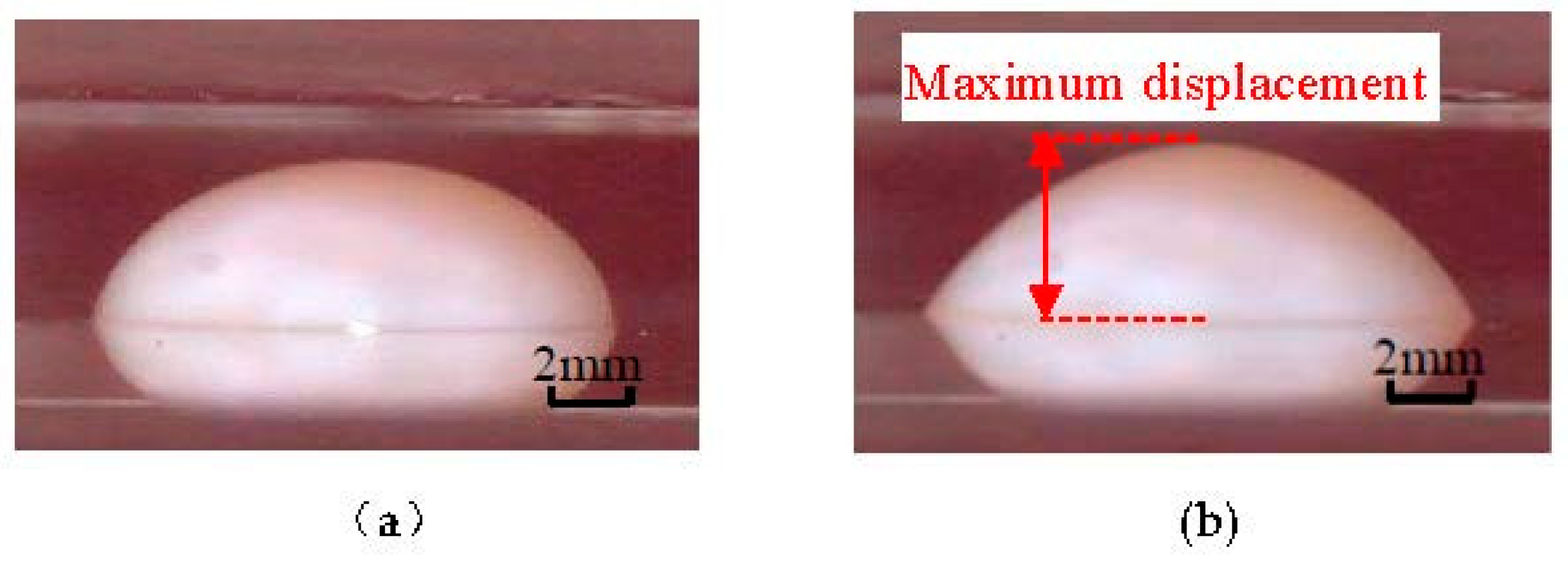
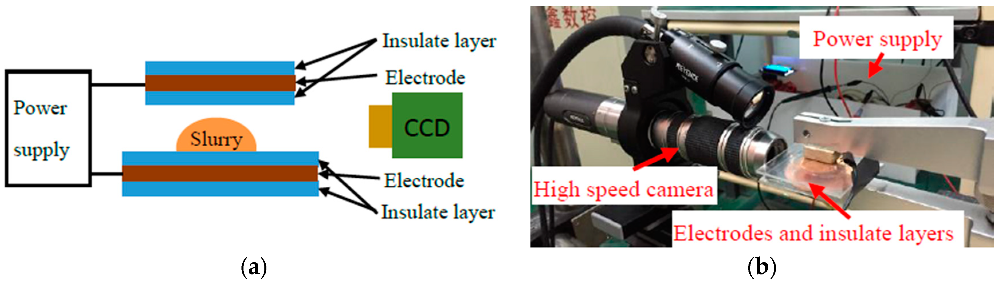
The movement of polishing slurry being acted upon by DEP force in a non-uniform electric field is observed in real-time by using a high-speed camera recording system, as shown in
Figure 7. The observing experimental results are shown in the
Figure 8. It could be seen from
Figure 8, compared with other frequencies, that the maximum movement displacement of the polishing slurry is achieved at the frequency of 40 Hz. The displacement of the polishing slurry at 40 Hz is shown in
Figure 9. Therefore, among these frequencies, when the frequency is 40 Hz, the largest DEP force is exerted on the polishing slurry. The 40 Hz was thus chosen as the frequency of subsequent processing experiments.
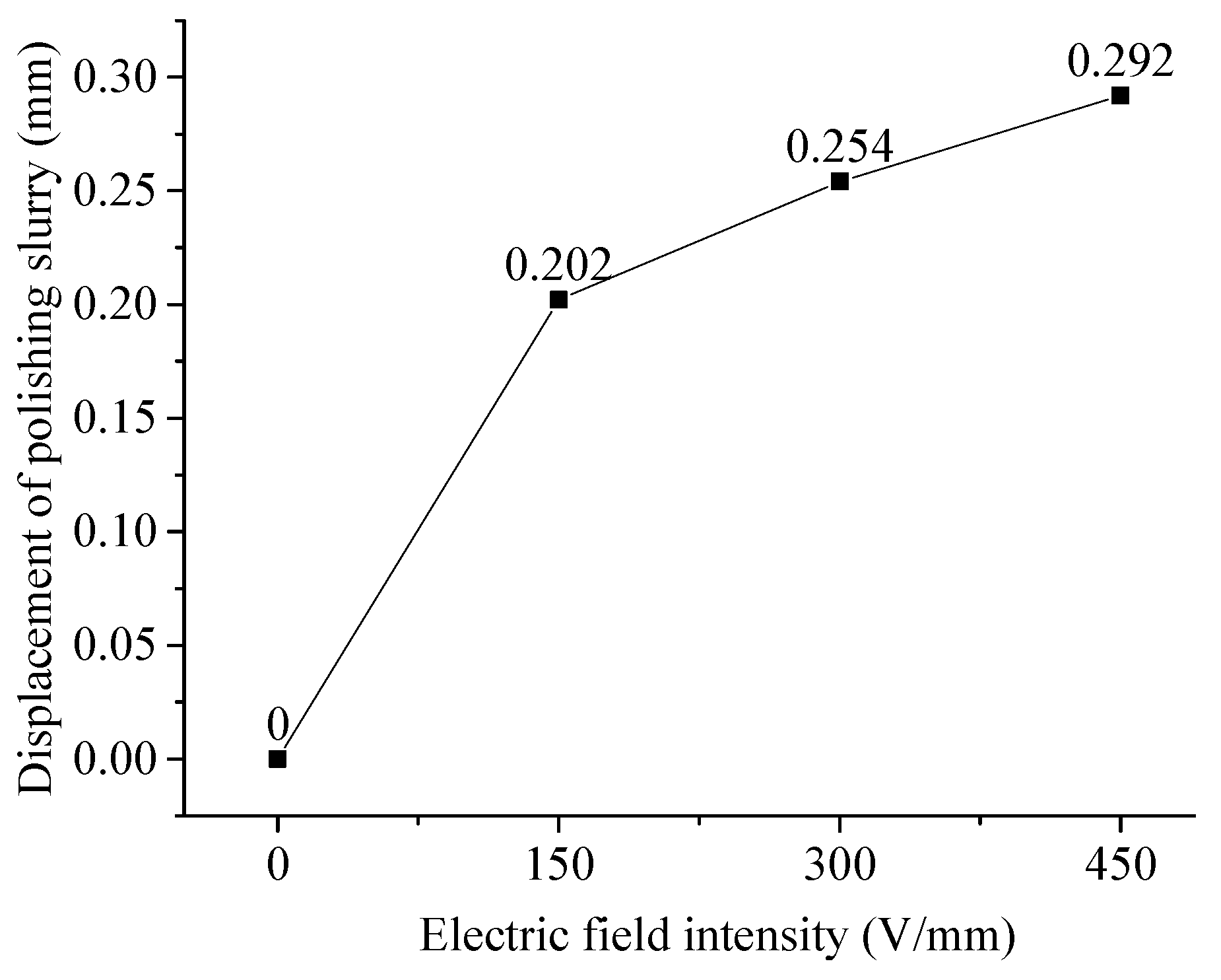
Figure 10 shows the maximum displacement of polishing slurry under different electric field intensities. It can be seen from the
Figure 10 that the electric field intensity is directly proportional to the displacement of the polishing slurry, the DEP effect and the DEP force on the polishing slurry. The DEP phenomenon is obvious at 300 V/mm, and the displacement of the polishing slurry at 300 V/mm is close to that of 450 V/mm. In fact, 450 V/mm is the maximum electric field intensity of the power supply, and considering the stability and reliability of the power supply, 300 V/mm was chosen as the electric field intensity for polishing experiments.
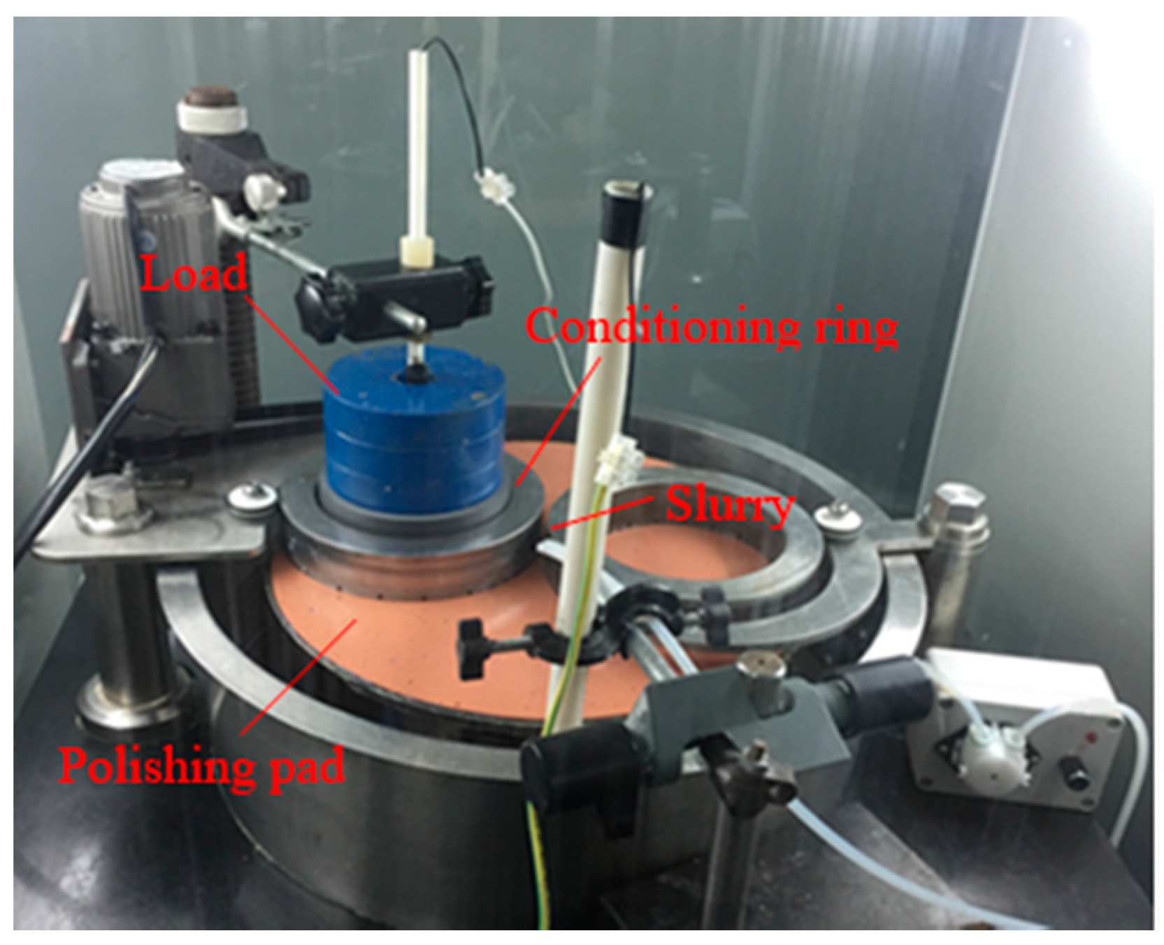
There were two groups of polishing experiments, one group utilized DEPP for sapphire substrate polishing, and the other group utilized traditional CMP. Most experimental settings for both groups were the same, the only difference between the two experiments being whether there is a non-uniform electric field. Detailed setting parameters for both experiments are shown in
Table 1. The experiments were carried out on a Nanopoli-100 precision polishing machine and
Figure 11 shows the picture of the actual DEPP machine. Turning off the power supply switches the machine to a traditional CMP polishing machine. The polishing pad is a cross-patterned polyurethane pad and its parameters are listed in
Table 2. The diameter and thickness of the sapphire substrates used in both experiments are 2 inches and 0.45 mm, respectively. The initial surface roughness of both substrates is about 1μm.
Figure 12 shows the initial surface morphology and micrographs of the substrates, and it can be seen that there are many damages on the surface.
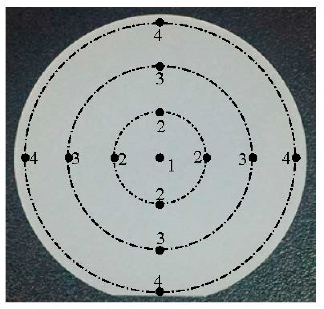
Four diameters (0 mm, 16 mm, 32 mm and 48 mm) were selected as the research objects, and four locations were marked at every same diameter on the sapphire surface, the marked locations shown in
Figure 13. The surface roughness of the marked locations was measured every 30 min; add the four surfaces roughness values at the same diameter, then the average surface roughness of each diameter was achieved. The measuring equipment was a VEECO white light interferometer. The change of surface roughness of sapphire at different diameters can be obtained from the average surface roughness. The surface morphology and the flatness of the sapphire substrates are observed after polishing. Initial weight and thickness of sapphire substrates are M and H, respectively. The weight after polishing is
M0, polishing time is t, and
MRR is the material removal rate:
5. Results and Discussion
The results from the polishing experiments indicated that the material removal rate, surface roughness and surface flatness of the two sapphire substrates are different in value, though these values are initially the same for both substrates.
5.1. Material Removal Rate
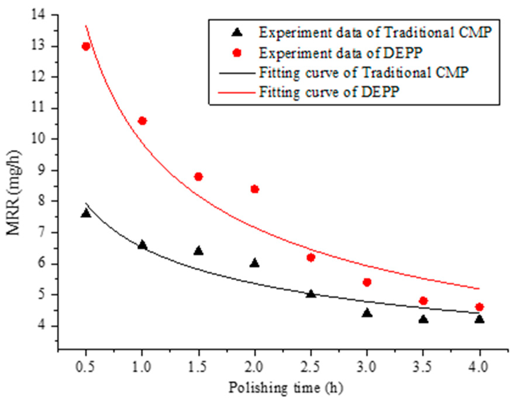
Figure 14 shows the
MRR comparison between the traditional CMP and the DEPP at different processing times; the dotted points in the graph are from the experimental data, and the curved lines show their fittings. From
Figure 14, it can be seen that the
MRR of sapphire substrates gradually decrease as time increases. This is due to the fact that during the initial polishing stage, the process mainly removes small protrusions generated by the former process, and the actual polishing area is extremely small. Therefore, the pressure is high. With the polished surface area increasing, the corresponding pressure decreases, so does the
MRR.
Comparing the two polishing methods, the MRR of DEPP was significantly higher than that of the traditional CMP. The maximum increase is 71%, reaching 13 mg/h, and the minimum increase is 9.5%, reaching 4.6 mg/h. The reason behind this is that, subject to DEP force, the abrasives will move towards to and congregate on the surface of the sapphire substrate, increasing the number of abrasives that participate in polishing. In the same time, the movement of abrasives increases the pressure between the sapphire substrate and polishing slurry. The ability of removing the soft layer formed by chemical action is also improved. Therefore, the DEPP method greatly improves the polishing efficiency.
5.2. Surface Roughness
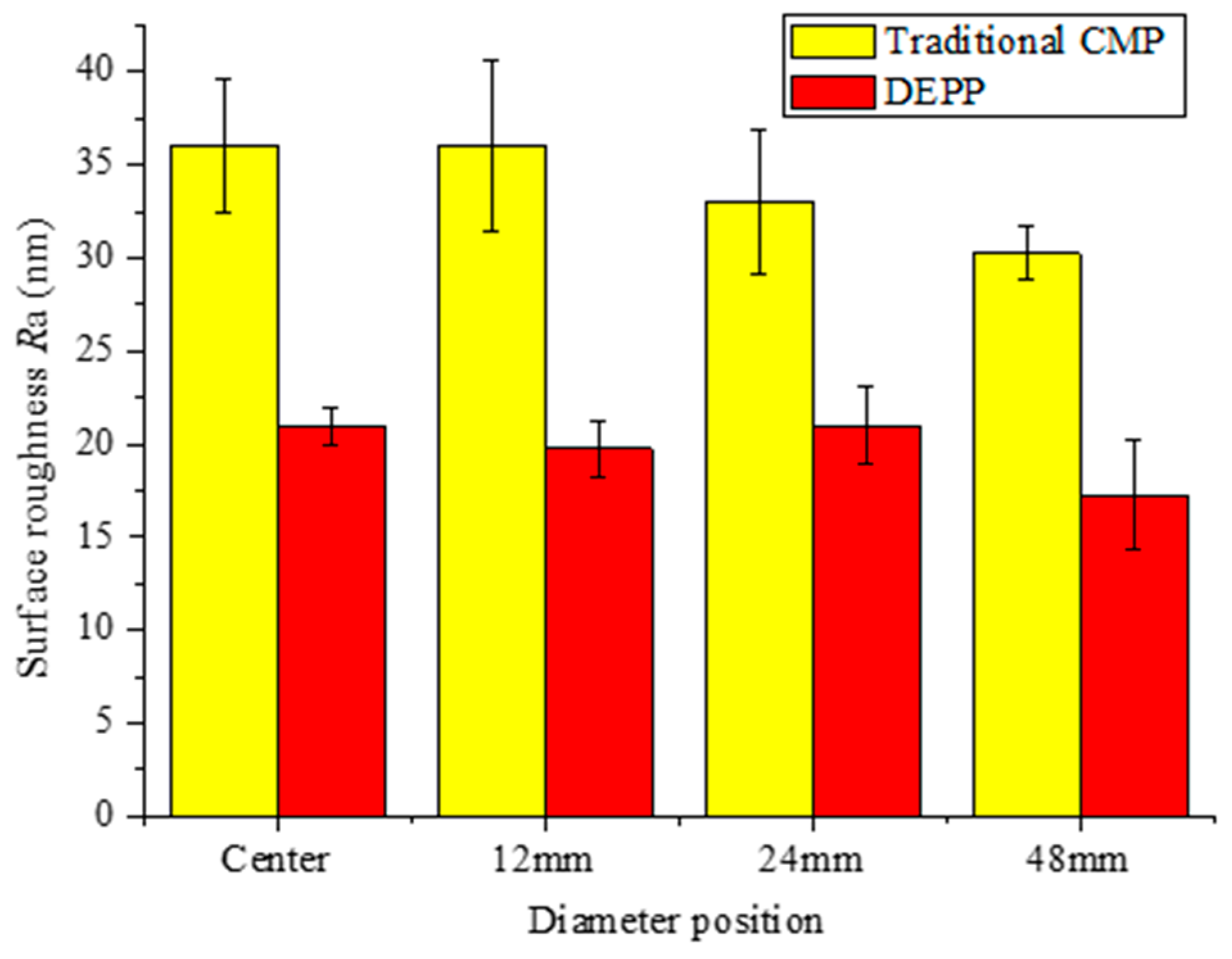
Figure 15 shows the average surface roughness of a sapphire substrate at different diameters after being polished for 4 h. It can be seen from the figure that the sapphire substrate polished by DEPP has lower roughness compared to that polished by the traditional CMP method. Due to high efficiency in the material removal rate of DEPP compared to that of CMP, it is expected that after the same amount of polishing time, a substrate polished using DEPP will have a better roughness value compared to that of CMP. On the other hand, the surface roughness decreases faster at larger diameter location when using traditional CMP. The reason for this can be explained by the “edge collapse” effect in flat polishing [
22]. The polishing pad is usually made of soft materials, and under the load action, deformation will occur, resulting in an uneven distribution of pressure on the sapphire substrate surface [
23]. The pressure at the edge of the sapphire substrate surface is greater than that at the center and stress concentration is more prominent at the edge. These factors lead to smaller roughness at the edge [
24]. However, edge surface roughness of the sapphire substrate is slightly lower than that at the center after DEPP and, therefore, no clear trend can be observed for roughness changing from high to low while moving from the center to the edge of the substrate. This is due to the fact that the DEP force slows down the polishing slurry thrown out in center area by centrifugal force, and increases the material removal at the center region of the sapphire substrate. Therefore, the roughness is relatively uniform at different diameter locations.
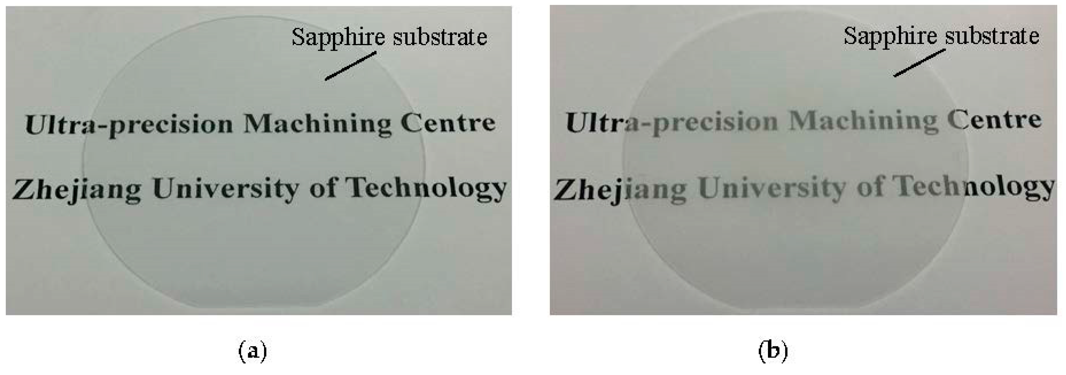
Figure 16 shows the sapphire substrates after polishing for 5 h with two polishing methods.
Figure 16a is sapphire substrate polished by the DEPP method, and the sapphire substrate in
Figure 16b was polished using the traditional CMP method. It can be seen from the figure that the transparency (surface roughness) after using the DEPP method to process the sapphire substrates is obviously better than that using the traditional CMP method. After processing for 5 h by DEPP, the surface roughness of sapphire at different diameters are all less than 1 nm.
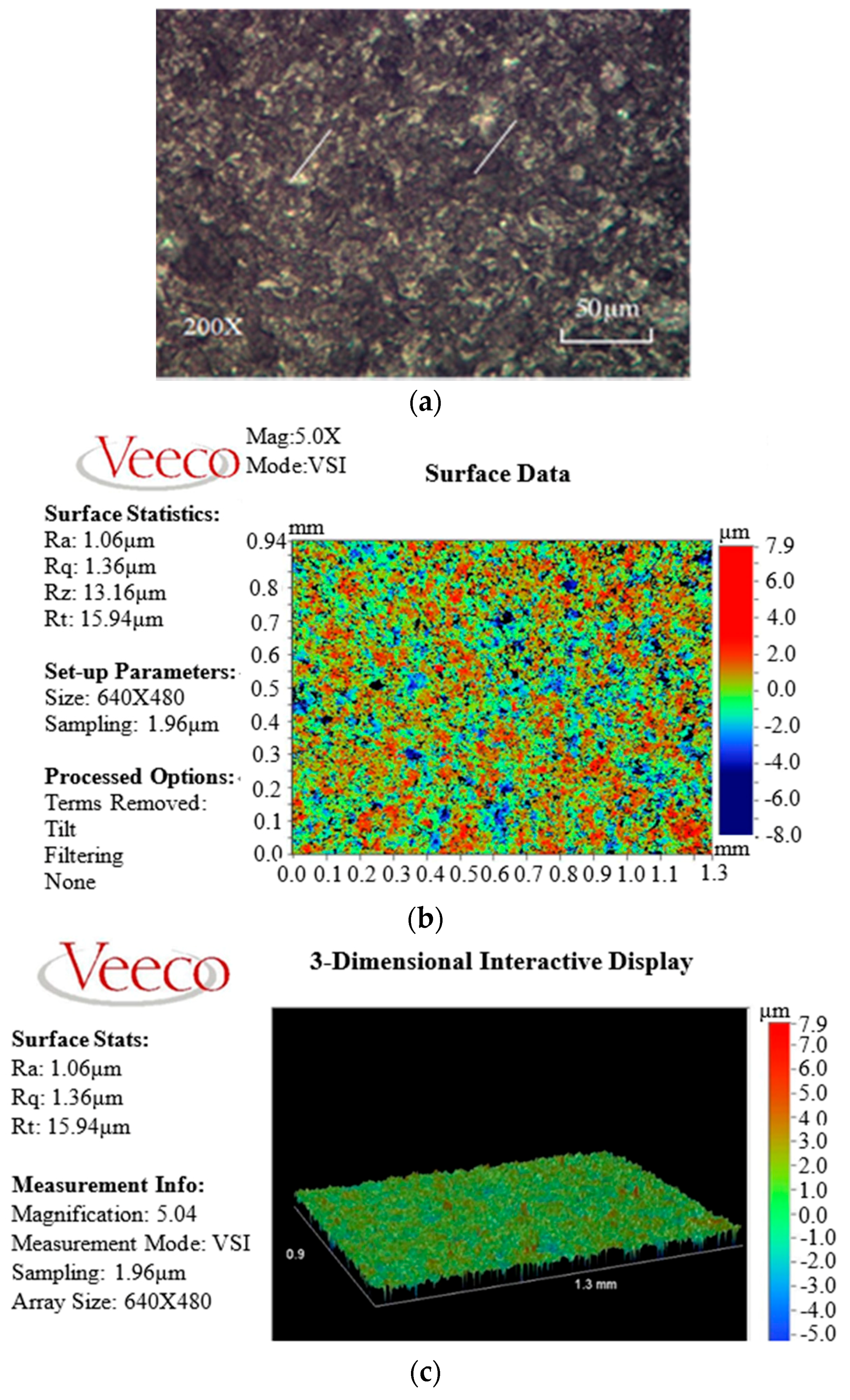
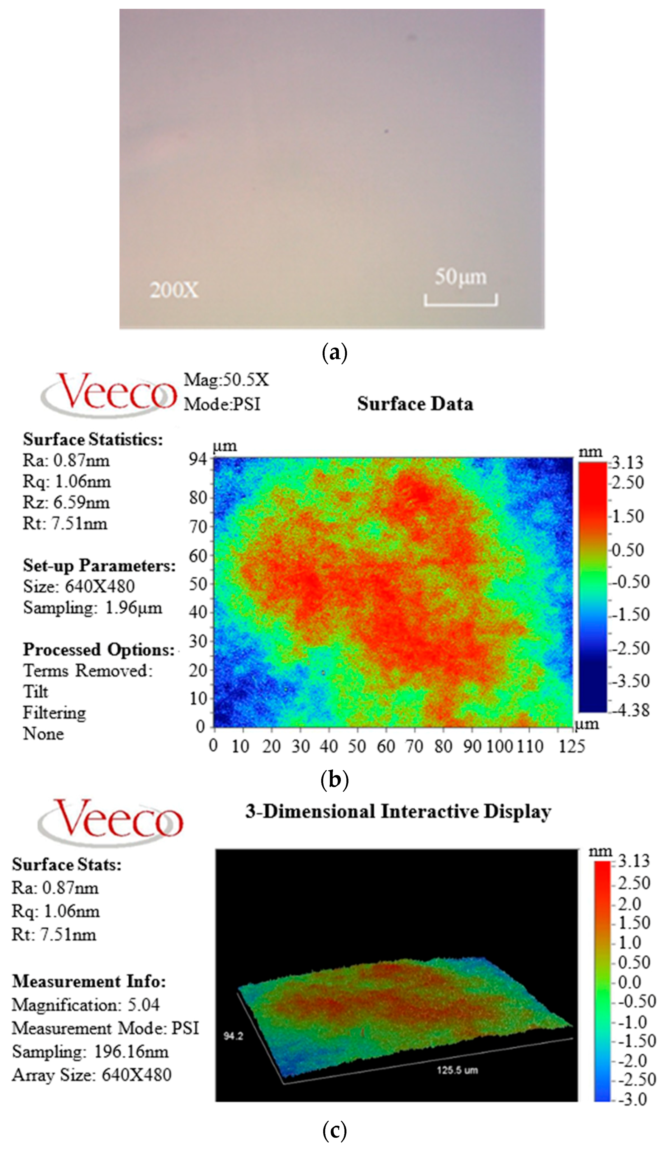
Figure 17 shows the final surface micrograph, roughness and morphology of the sapphire substrate surface; the surface damage has been eliminated, and the surface roughness is
Ra 0.87 nm.
5.3. Flatness
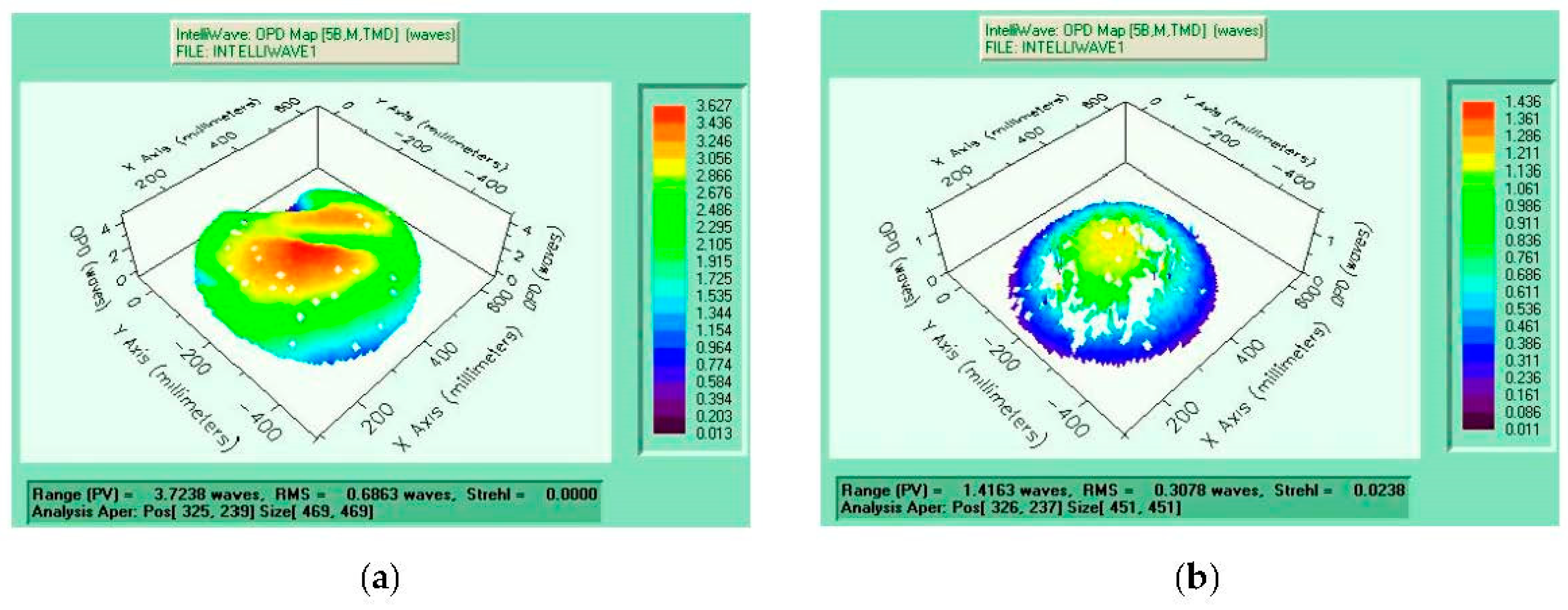
With DEPP and traditional CMP, the flatness of the sapphire substrates is shown in
Figure 18. For substrate polished with traditional CMP, its height increases from the edge to the center, with the center significantly higher than other locations. The flatness (RMS value) of the substrate is 0.6863 waves. While with DEPP, the height of the substrate also gradually increases from the edge to the center, however with a much smaller magnitude. The flatness (RMS value) is 0.3078 waves. Thus, it can be concluded that the polished sapphire substrate surface obtained by DEPP is smoother and flatter than that by traditional CMP.
The reason why the flatness of the sapphire substrate polished by DEPP is better than that polished by the traditional CMP is similar to that for surface roughness. Abrasives move in the direction towards the sapphire substrate and congregate on the surface of the substrate, and this effectively increases the friction between the polishing slurry and the sapphire substrate, slowing down the effect of the polishing slurry thrown out by centrifugal force. Comparing with the traditional CMP, the polishing slurry on the sapphire substrate surface is distributed more evenly in the DEPP process and there are more abrasives participating in material removal at the central location. Therefore, DEPP results in better flatness compared to the traditional CMP.
6. Conclusions
Adding asymmetric electrodes in a traditional polishing machine to form a non-uniform electric field in the polishing area generates a DEP effect, and such effect drives abrasives to assist polishing sapphire substrates.
Experimental results show that DEPP can improve MRR, surface roughness uniformity and surface flatness for sapphire substrates. Compared with traditional CMP, DEPP can improve sapphire substrate MRR by 71% in maximum and 9.5% in minimum, reaching 13 mg/h and 4.6 mg/h for MRR, respectively. It was found that the surface roughness of the sapphire substrate decreases faster with better uniformity during the DEPP process, and the final surface roughness is Ra 0.87 nm. The flatness of the sapphire substrate polished by DEPP is 0.3078 waves (RMS value), a great improvement compared to 0.6863 waves (RMS value) with traditional CMP. The abrasives move in the direction towards the plate by the DEP force, resulting in an increase in pressure and friction between the polishing slurry and the sapphire substrate, decreasing in the thrown-out effect of the polishing slurry by centrifugal force, and an improvement in polishing uniformity. On the other hand, with more abrasives participating in the polishing process, the ability to remove the soft layer produced by chemical reaction is enhanced and polishing efficiency is improved. Therefore, the DEPP is a highly efficient, high precision polishing method for sapphire substrates.

 ,
, 


