Oblique Wide-Angle Multi-Sector Metamaterial Absorber for Space Applications


Abstract
Featured Application
Abstract
1. Introduction
2. Design
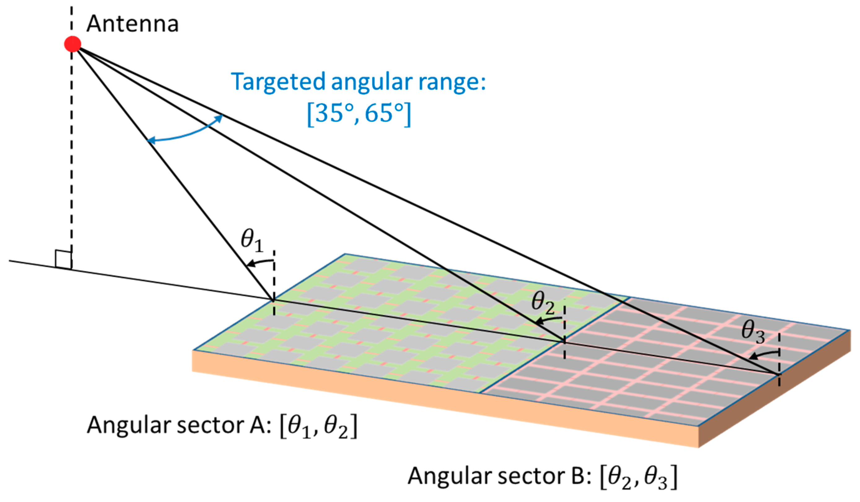
2.1. Sectorial Absorber Concept and Objective
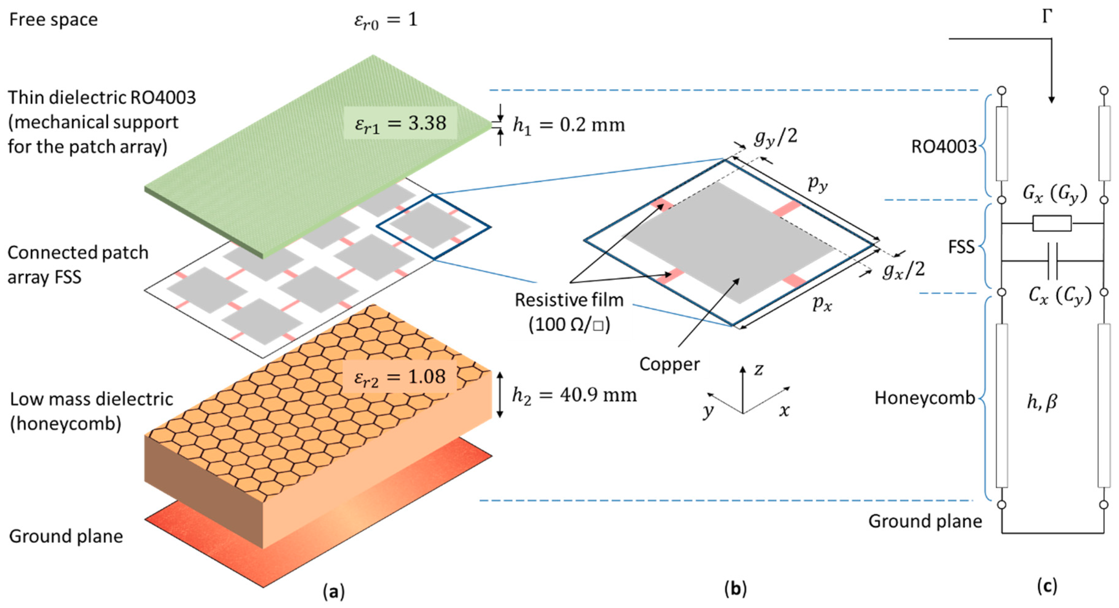
2.2. Description of the Absorbers
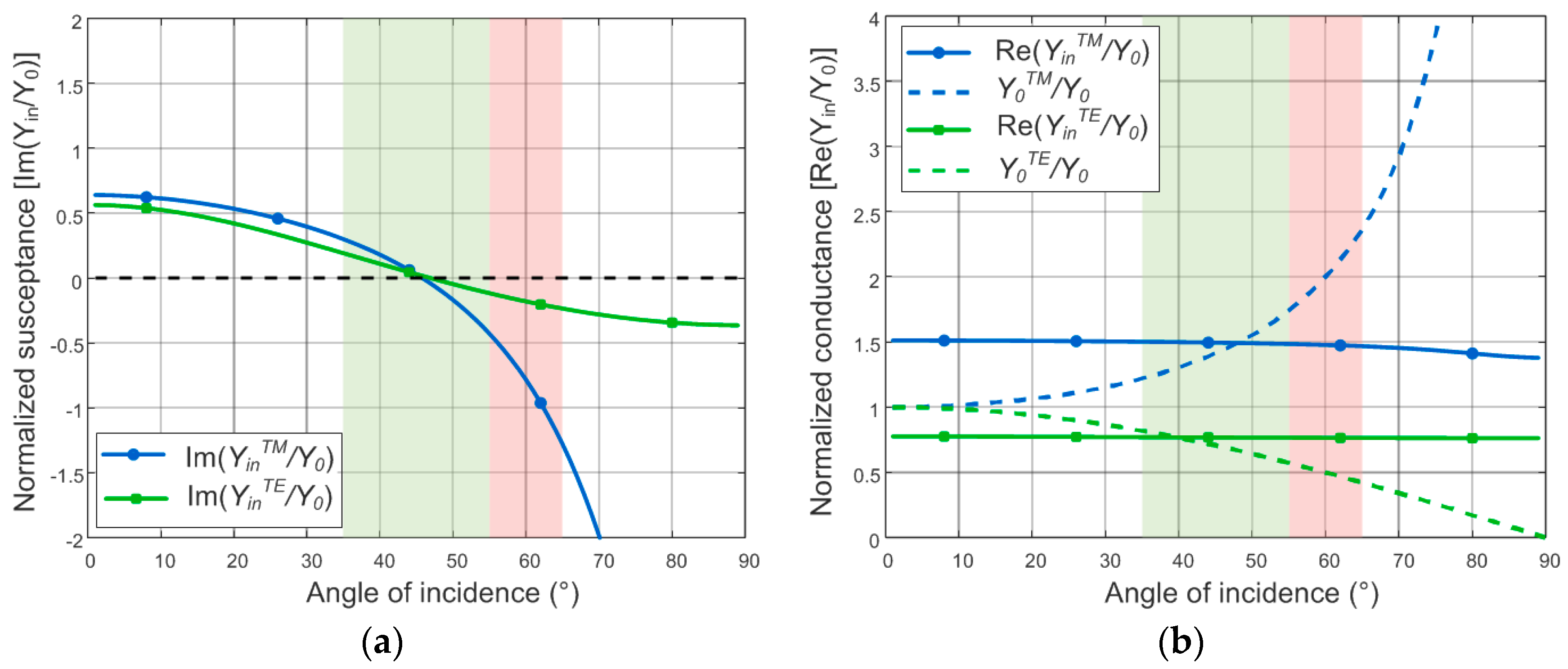
2.3. Optimization of Sector A
- -
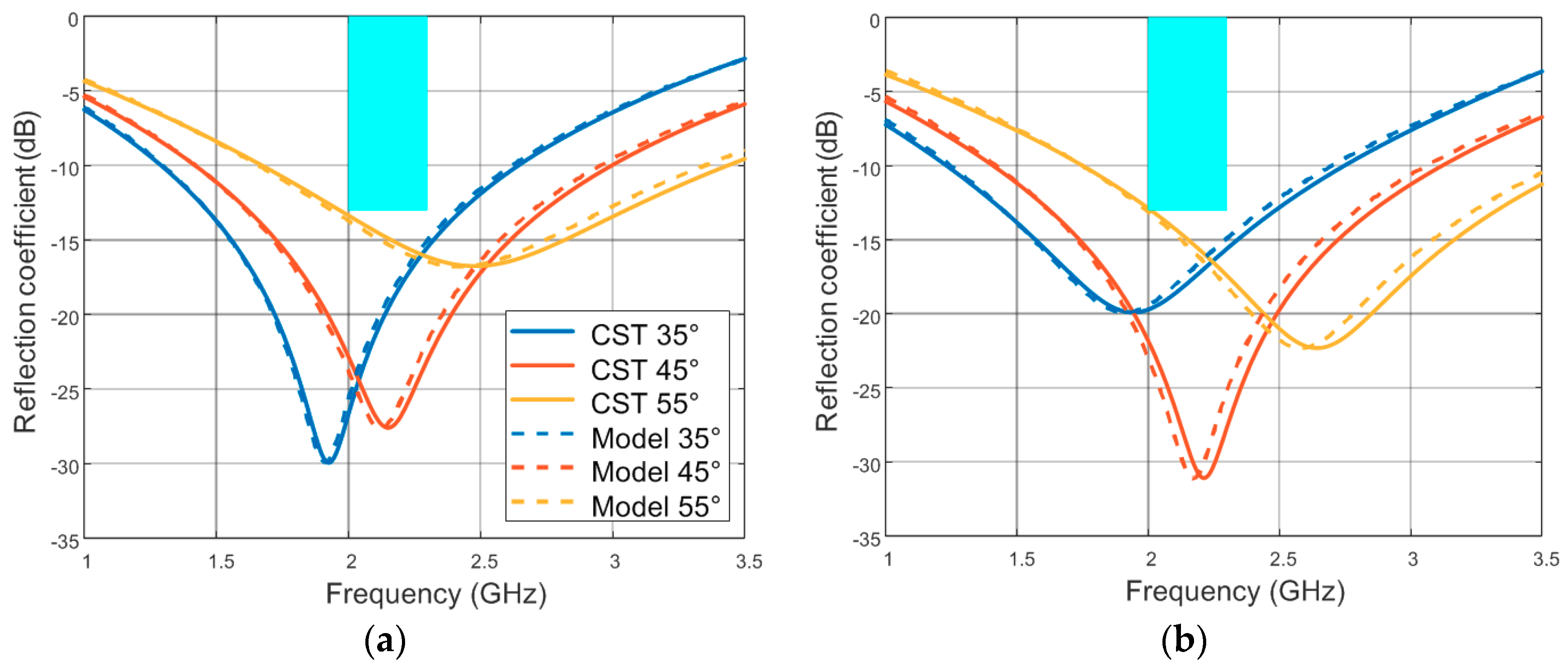
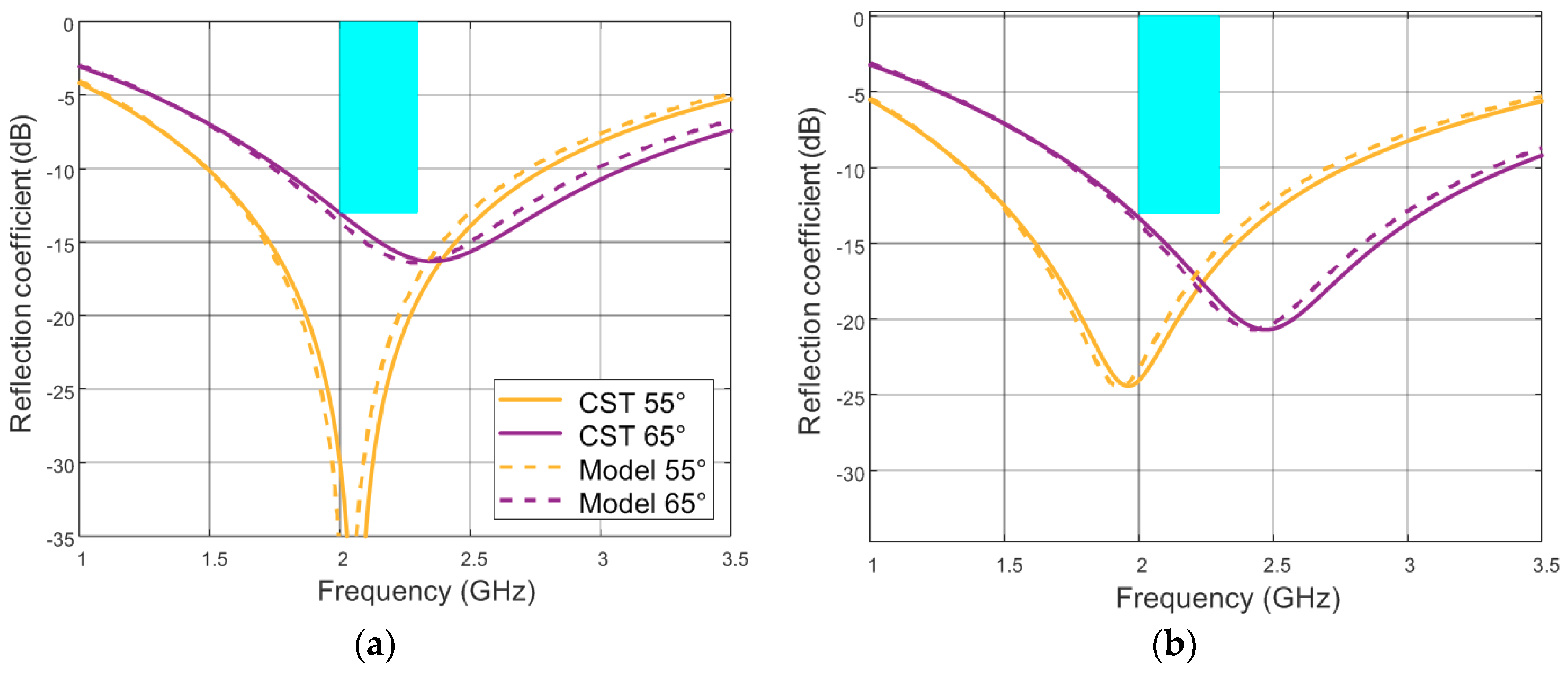
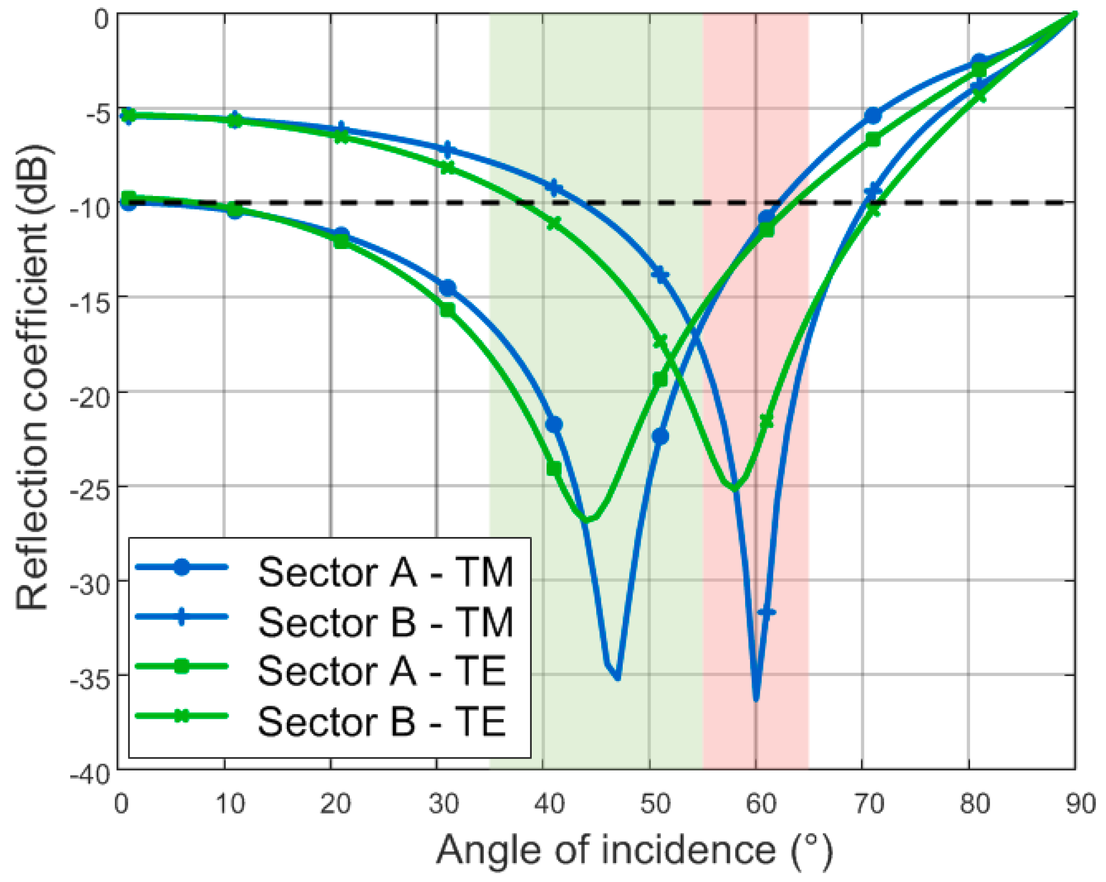
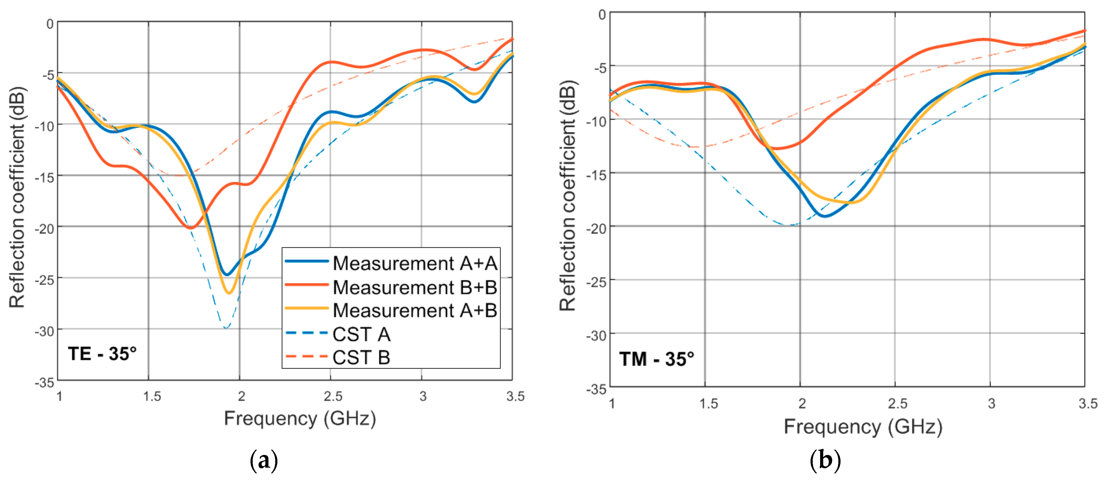
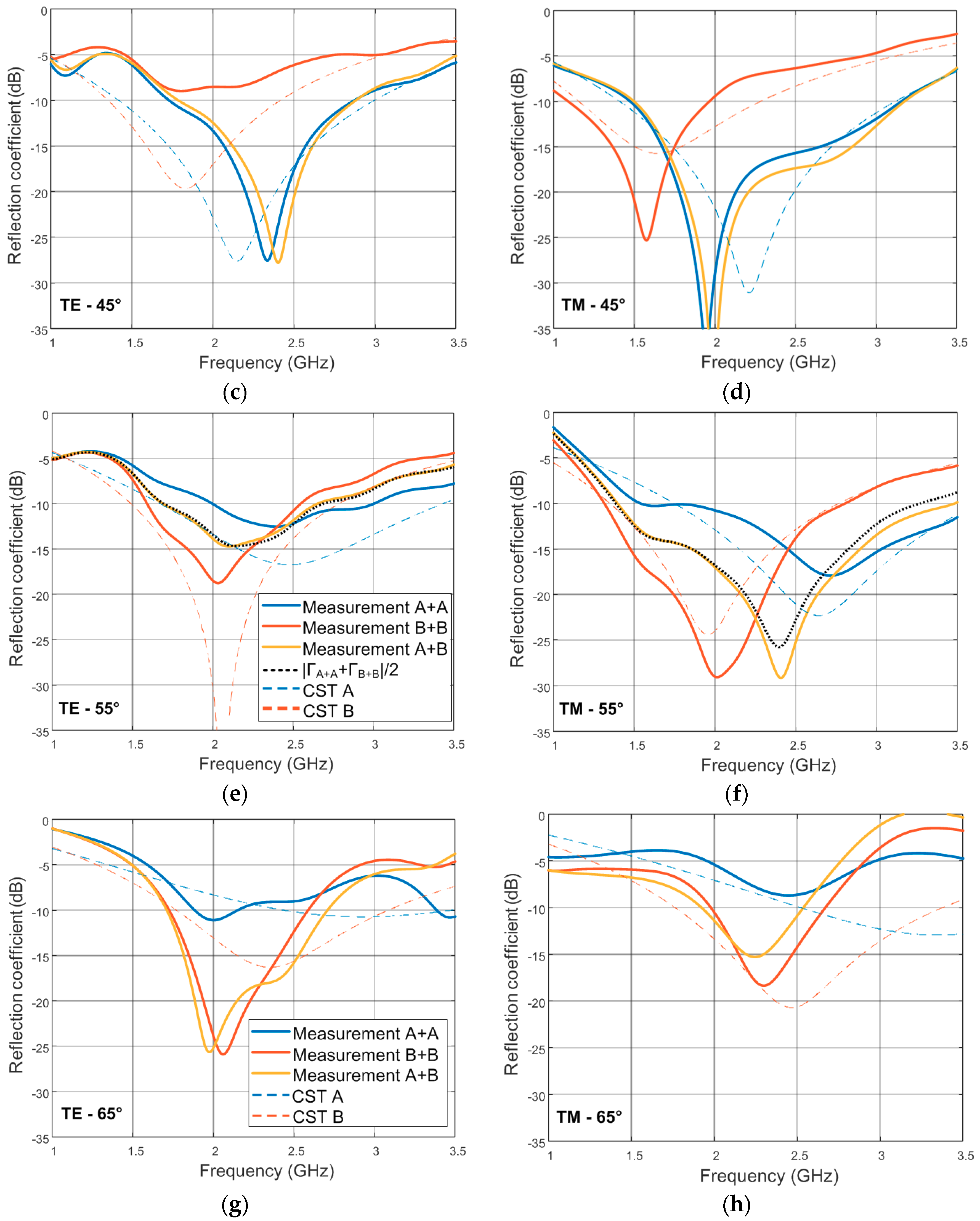
- The resonant frequency, for which the reflection is minimum, shifts toward high frequency for increasing angles. For TE (Figure 3a), we observed a shift from 1.9 GHz to 2.5 GHz for 35° and 55° respectively.
- -
- The absorption level varies with . For TE, we observe that the absorption ranges from −30 dB to −15 dB for 35° and 55°, respectively.
2.4. Optimization of Sector B
3. Measurement
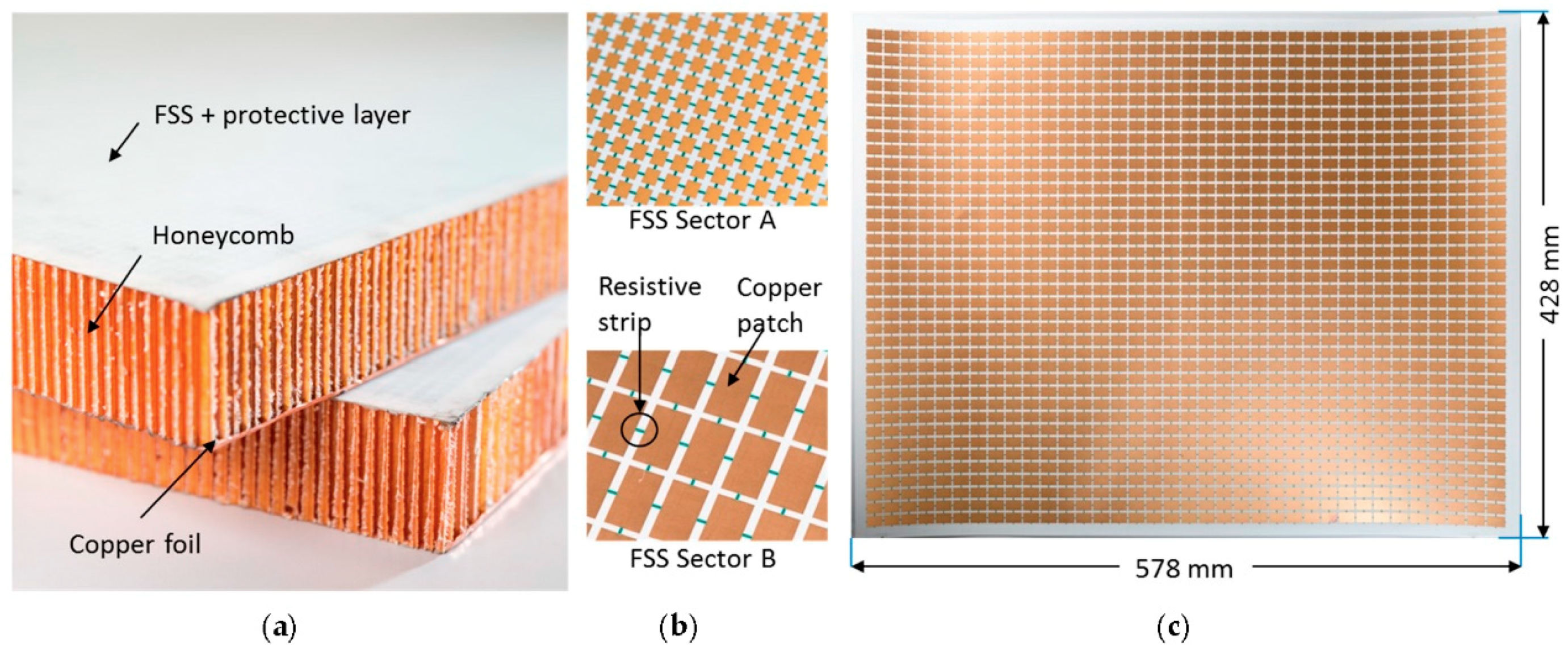
3.1. Prototypes
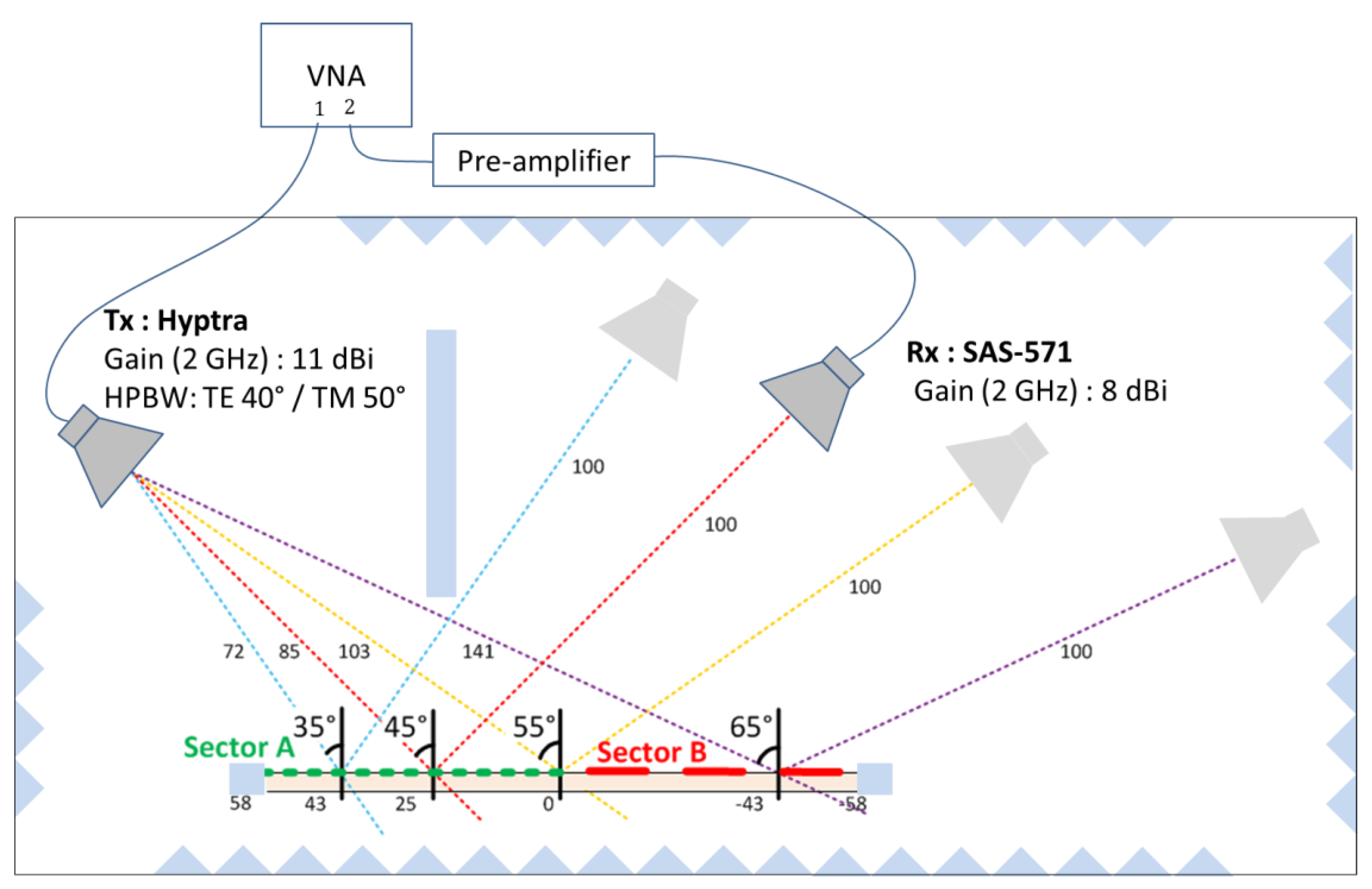
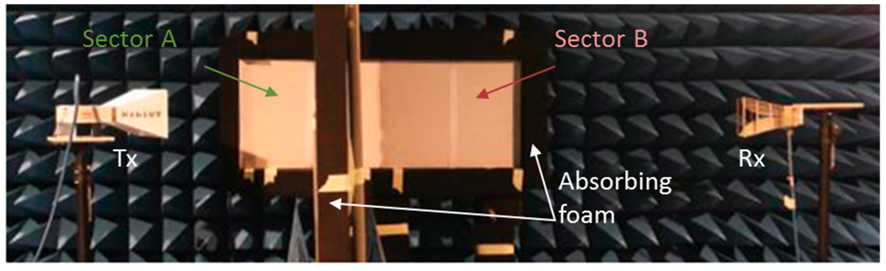
3.2. Measurement Setup
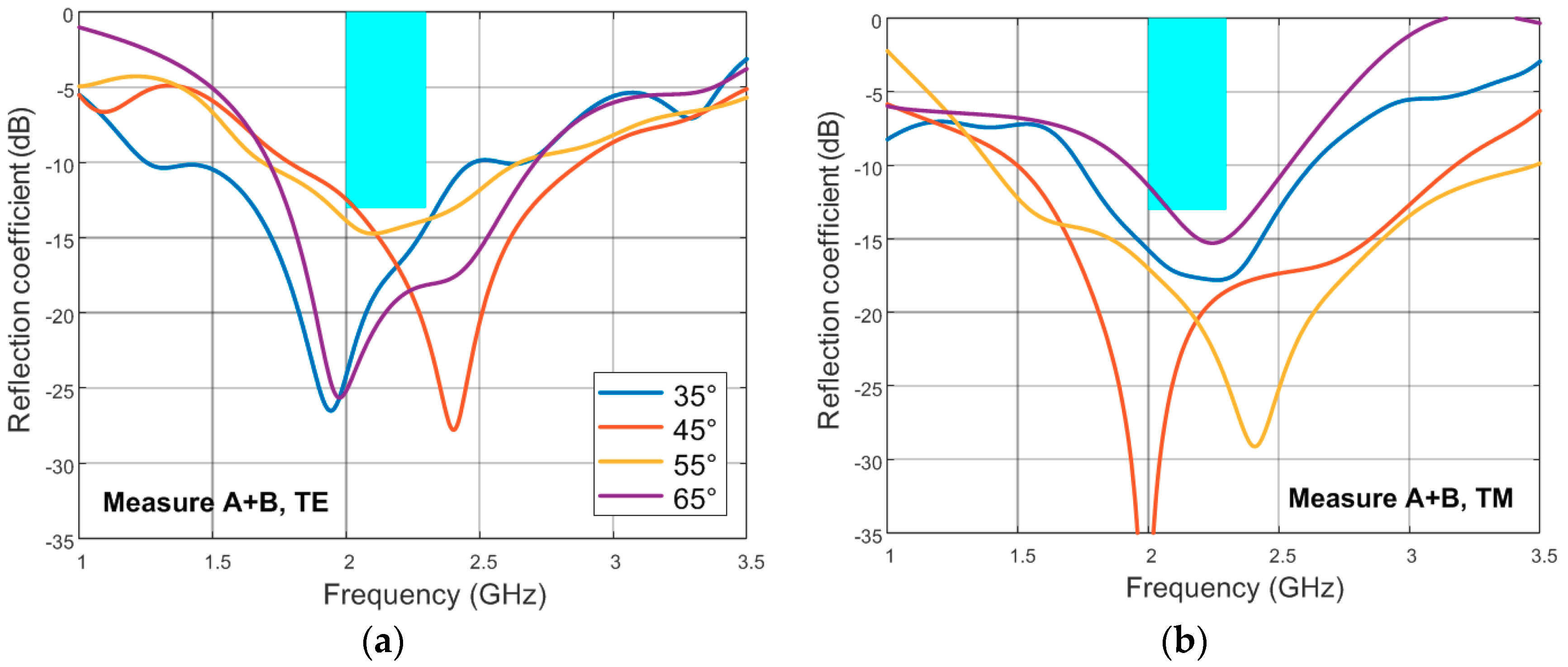
3.3. Measurement Results
4. Conclusions
Author Contributions
Funding
Conflicts of Interest
References
- Martel, C.; Gabard, B.; Boust, F.; Gobin, V.; Elis, K. A metamaterial electromagnetic wave absorber based on resistive films for micro-satellite spatial applications. In Proceedings of the 2018 IEEE International Symposium on Antennas and Propagation USNC/URSI National Radio Science Meeting, Boston, MA, USA, 8–13 July 2018; pp. 441–442. [Google Scholar]
- Delfini, A.; Albano, M.; Vricella, A.; Santoni, F.; Rubini, G.; Pastore, R.; Marchetti, M. Advanced radar absorbing ceramic-based materials for multifunctional applications in space environment. Materials 2018, 11, 1730. [Google Scholar] [CrossRef] [PubMed]
- Salisbury, W.W. Absorbent body for electromagnetic waves. U.S. Patent 2599944, 10 June 1952. [Google Scholar]
- Toit, L.J.D. The design of Jauman absorbers. IEEE Antennas Propag. Mag. 1994, 36, 17–25. [Google Scholar] [CrossRef]
- Engheta, N. Thin absorbing screens using metamaterial surfaces. In Proceedings of the IEEE Antennas and Propagation Society International Symposium, San Antonio, TX, USA, 16–21 June 2002; pp. 392–395. [Google Scholar]
- Munk, B.A. Frequency Selective Surfaces—Theory and Design; Wiley-Blackwell: New York, NY, USA, 2000. [Google Scholar]
- Lee, D.; Hwang, J.G.; Lim, D.; Hara, T.; Lim, S. Incident angle- and polarization-insensitive metamaterial absorber using circular sectors. Sci. Rep. 2016, 6, 27155. [Google Scholar] [CrossRef] [PubMed]
- Wang, J.; Yang, R.; Tian, J.; Chen, X.; Zhang, W. A dual-band absorber with wide-angle and polarization insensitivity. IEEE Antennas Wirel. Propag. Lett. 2018, 17, 1242–1246. [Google Scholar] [CrossRef]
- Kalraiya, S.; Chaudhary, R.K.; Abdalla, M.A. Design and analysis of polarization independent conformal wideband metamaterial absorber using resistor loaded sector shaped resonators. J. Appl. Phys. 2019, 125, 134904. [Google Scholar] [CrossRef]
- Nguyen, T.T.; Lim, S. Wide incidence angle-insensitive metamaterial absorber for both TE and TM polarization using eight-circular-sector. Sci. Rep. 2017, 7, 3204. [Google Scholar] [CrossRef] [PubMed]
- Munk, B.A.; Munk, P.; Pryor, J. On designing jaumann and circuit analog absorbers (CA absorbers) for oblique angle of incidence. IEEE Trans. Antennas Propag. 2007, 55, 186–193. [Google Scholar] [CrossRef]
- Alvarez, H.F.; de Cos Gomez, M.E.; Las-Heras, F. Angular stability of metasurfaces: challenges regarding reflectivity measurements. IEEE Antennas Propag. Mag. 2016, 58, 74–81. [Google Scholar] [CrossRef]
- Pinto, Y.; Sarrazin, J.; Lepage, A.C.; Begaud, X.; Capet, N. Design and measurement of a thin and light absorbing material for space applications. App. Phys. A 2014, 115, 541–545. [Google Scholar] [CrossRef]
- Pinto, Y.; Sarrazin, J.; Lepage, A.C.; Begaud, X.; Capet, N. Resistive high-impedance surfaces (RHIS) as absorbers for oblique incidence electromagnetic waves. Appl. Phys. A 2014, 117, 693–697. [Google Scholar] [CrossRef]
- Capet, N.; Ballesteros, Y.C.P.; Lepage, A.C.; Sarrazin, J.; Begaud, X. Multi-Sector Absorbing Method and Device. U.S. Patent WO2015136121, 17 September 2015. [Google Scholar]
- Lepage, A.C.; Pinto, Y.; Rance, O.; Begaud, X.; Capet, N. Lightweight and Wide-Angle Metamaterial Absorbing Material Concept. In Proceedings of the European Conference on Antennas and Propagation (EuCAP 2018), London, UK, 9–13 April 2018. [Google Scholar]
- Luukkonen, O.; Simovski, C.; Granet, G.; Goussetis, G.; Lioubtchenko, D.; Raisanen, A.V.; Tretyakov, S.A. Simple and Accurate Analytical Model of Planar Grids and High-Impedance Surfaces Comprising Metal Strips or Patches. IEEE Trans. Antennas Propag. 2008, 56, 1624–1632. [Google Scholar] [CrossRef]
- Magill, E.; Wheeler, H. Wide-angle impedance matching of a planar array antenna by a dielectric sheet. IEEE Trans. Antenn. Propag. 1966, 14, 49–53. [Google Scholar] [CrossRef]
- Costa, F.; Monorchio, A.; Manara, G. Efficient Analysis of Frequency-Selective Surfaces by a Simple Equivalent-Circuit Model. IEEE Trans. Antennas Propag. 2012, 54, 35–48. [Google Scholar] [CrossRef]
- Chambers, B. Optimum design of a Salisbury screen radar absorber. Electron.Lett. 1994, 30, 1353–1354. [Google Scholar] [CrossRef]
- Hiatt, R.E.; Knott, E.F.; Senior, T.B.A. A Study of VHF Absorbers and Anechoic Rooms; Report No. 5391-1-F; The University of Michigan/NASA, Langley Research Center: Hampton, VA, USA, 1963.
- Paquay, M.; Iriarte, J.; Ederra, I.; Gonzalo, R.; Maagt, P. de Thin AMC structure for radar cross-section reduction. IEEE Trans. Antennas Propag. 2007, 55, 3630–3638. [Google Scholar] [CrossRef]


| p (mm) | g (mm) | w (mm) | Z (Ω) | |
|---|---|---|---|---|
| TE (x) | 5.1 | 1.6 | 0.32 | 500 |
| TM (y) | 5 | 1 | 0.4 | 250 |
| p (mm) | g (mm) | w (mm) | Z (Ω) | |
|---|---|---|---|---|
| TE (x) | 10.5 | 2 | 0.45 | 444 |
| TM (y) | 15.5 | 1.3 | 0.46 | 283 |
© 2019 by the authors. Licensee MDPI, Basel, Switzerland. This article is an open access article distributed under the terms and conditions of the Creative Commons Attribution (CC BY) license (http://creativecommons.org/licenses/by/4.0/).
Share and Cite
Rance, O.; Lepage, A.C.; Begaud, X.; Elis, K.; Capet, N. Oblique Wide-Angle Multi-Sector Metamaterial Absorber for Space Applications. Appl. Sci. 2019, 9, 3425. https://doi.org/10.3390/app9163425
Rance O, Lepage AC, Begaud X, Elis K, Capet N. Oblique Wide-Angle Multi-Sector Metamaterial Absorber for Space Applications. Applied Sciences. 2019; 9(16):3425. https://doi.org/10.3390/app9163425
Chicago/Turabian StyleRance, Olivier, Anne Claire Lepage, Xavier Begaud, Kevin Elis, and Nicolas Capet. 2019. "Oblique Wide-Angle Multi-Sector Metamaterial Absorber for Space Applications" Applied Sciences 9, no. 16: 3425. https://doi.org/10.3390/app9163425
APA StyleRance, O., Lepage, A. C., Begaud, X., Elis, K., & Capet, N. (2019). Oblique Wide-Angle Multi-Sector Metamaterial Absorber for Space Applications. Applied Sciences, 9(16), 3425. https://doi.org/10.3390/app9163425