Article

Adsorption and Sensing Behaviors of Pd-Doped InN Monolayer upon CO and NO Molecules: A First-Principles Study

Institute of Water Resources and Electric Power, Qinghai University, Xining 810016, China
*
Author to whom correspondence should be addressed.
Appl. Sci. 2019, 9(16), 3390; https://doi.org/10.3390/app9163390
Submission received: 24 July 2019 / Revised: 8 August 2019 / Accepted: 12 August 2019 / Published: 17 August 2019

Abstract

:
A transition metal (TM) doped InN monolayer has demonstrated with superior behavior for gas adsorption and sensing. For this paper, we studied the adsorption behavior of a Pd-doped InN (Pd-InN) monolayer upon CO and NO using the first-principles theory. Our results show that the Pd-InN monolayer has a stronger interaction with the CO molecule, compared with the NO molecule, with larger adsorption energy of 2.12 eV, compared to −1.65 eV. On the other hand, the Pd-InN monolayer undergoes more obvious deformation of the electronic behavior in the NO system, making the surface become semimetallic with a 0 eV band gap. Thus, the Pd-InN monolayer could be a promising candidate as a resistance-type sensor for NO detection and as a gas adsorbent for CO removal. We are hopeful that this work can offer the basic physicochemical properties and potential applications of the Pd-InN monolayer, which is beneficial for its further exploration in many fields.

1. Introduction

Very recently, two-dimensional (2D) materials have become the focus of attention in the academic community for potential applications in nanoelectronic devices, gas sensing, photo-catalysis, energy storage, and optical devices [1,2,3,4], because of their excellent physicochemical properties, including high electron mobility, high specific surface area, super-capacitors, as well as desirable optical properties. With the success of graphene in 2004 [5], scholars began to pursue other graphene-like nanomaterials with similar structures and properties [6,7], which largely facilitated the development of materials science. Among the novel members, the group III–V nitrides [8,9,10,11], including BN, AlN, and InN nanosheets, raise considerable attention for many applications due to their supreme semiconducting property.
Particularly, the InN monolayer has demonstrated superior thermal stability, high carrier mobility, and a sizable band gap [12,13,14]. Moreover, its large specific surface area and favorable chemical reactivity confers the potential application of the InN monolayer to be a gas sensor for typical gases. For example, the adsorption behavior of a pristine InN monolayer to several small gas molecules was implemented in a theoretical study [15], which implies its strong potential for sensing applications given the comparable performance with graphene. Chen [16] et al. investigated the Cu-doped InN monolayer for sensing decomposed SF6 species and found that it possesses enhanced behavior in comparison with the intrinsic counterpart. Guo [17] et al. proposed Pd, Pt, Ag, and Au decorated InN monolayers for NO2 sensing applications in order to exploit the potential of transition metal (TM) doped InN monolayers as toxic gas sensors. These findings suggest the InN monolayer is a promising sensing material and the TM-doped surface could be an even more extraordinary candidate for gas detection, as verified in the carbon-based surfaces [18,19] and transition metal dichalcogenides [20].
CO and NO are widely recognized as toxic gases that exert great threat to our living environment and to human health. Therefore, detection of these gases is significant for guaranteeing the living condition around us. Nanomaterials based on carbon nanotubes [21] and MoS2 monolayers [22] were proposed to realize this purpose and obtain desirable results, on which TM atoms largely contribute to enhancing the sensitivity of nano surfaces. To the best of our knowledge, there has been no report regarding a TM-doped InN monolayer for adsorption and sensing such two toxic species. In this regard, we studied the adsorption and sensing behaviors of the Pd-doped InN (Pd-InN) monolayer upon CO and NO gases by the first-principles theory, in order to shed light on the potential of the Pd-InN monolayer for gas sensing exploration. Based on our calculations, it could be concluded that Pd-InN is a promising candidate to detect NO and scavenger CO, which may facilitate the development of resistance-type sensors or gas adsorbents for applications in environment monitoring and industrial manufacturing.

2. Computational Details

We implemented the whole theoretical calculation, namely the structural relaxation and electronic calculation, in the dispersion-corrected DMol3 package based on density functional theory (DFT) [23]. To obtain the accurate electronic behavior of the analyzed systems, generalized gradient approximation, within the Perdew–Burke–Ernzerhof (GGA-PBE) function and in line with the HSE06 function, was adopted to treat the electron exchange-correlation interaction for comparison [24]. It is known that PBE may underestimate the bandgap, while HSE06 may slightly overestimate it. The DFT-D method proposed by Grimme was employed to better understand the Van der Waals force and long-range interactions [25,26]. Double numerical plus polarization (DNP) was selected as the atomic orbital basis set, with a global orbital cut-off radius of 5.0 Å in order to ensure the accuracy of total energy [27,28]. In terms of Monkhorst–Pack k-point setting, we determined 7 × 7 × 1 for geometric optimizations and 10 × 10 × 1 electronic structure calculations [29].
A 4 × 4 × 1 supercell of the InN monolayer was established, which contains 16 In atoms and 16 N atoms, with a vacuum region of 15 Å to prevent the interaction between adjacent units. The lattice constant of the InN monolayer calculated in this work was 3.62 Å, consistent with the previous work (3.63 Å [30]).
To evaluate the adsorption strength of the Pd-InN monolayer towards gas molecules, the adsorption energy (Ead) is determined, expressed as follows: Ead = EPd-InN + EgasEPd-InN/gas, where EPd-InN and EPd-InN/gas represent the total energy of the Pd-InN monolayer before and after gas adsorption and the Egas is the energy for isolated CO or NO molecules. It is undoubtable that a negative Ead represents the exothermicity of the gas adsorption process. Additionally, the Hirshfeld method is used to consider the charge transfer (QT) between the Pd-InN monolayer and gas molecules, defined as the charge of the adsorbed gaseous species. Based on this definition, a positive QT represents the electron-losing property of related gas molecule.

3. Results and Discussion

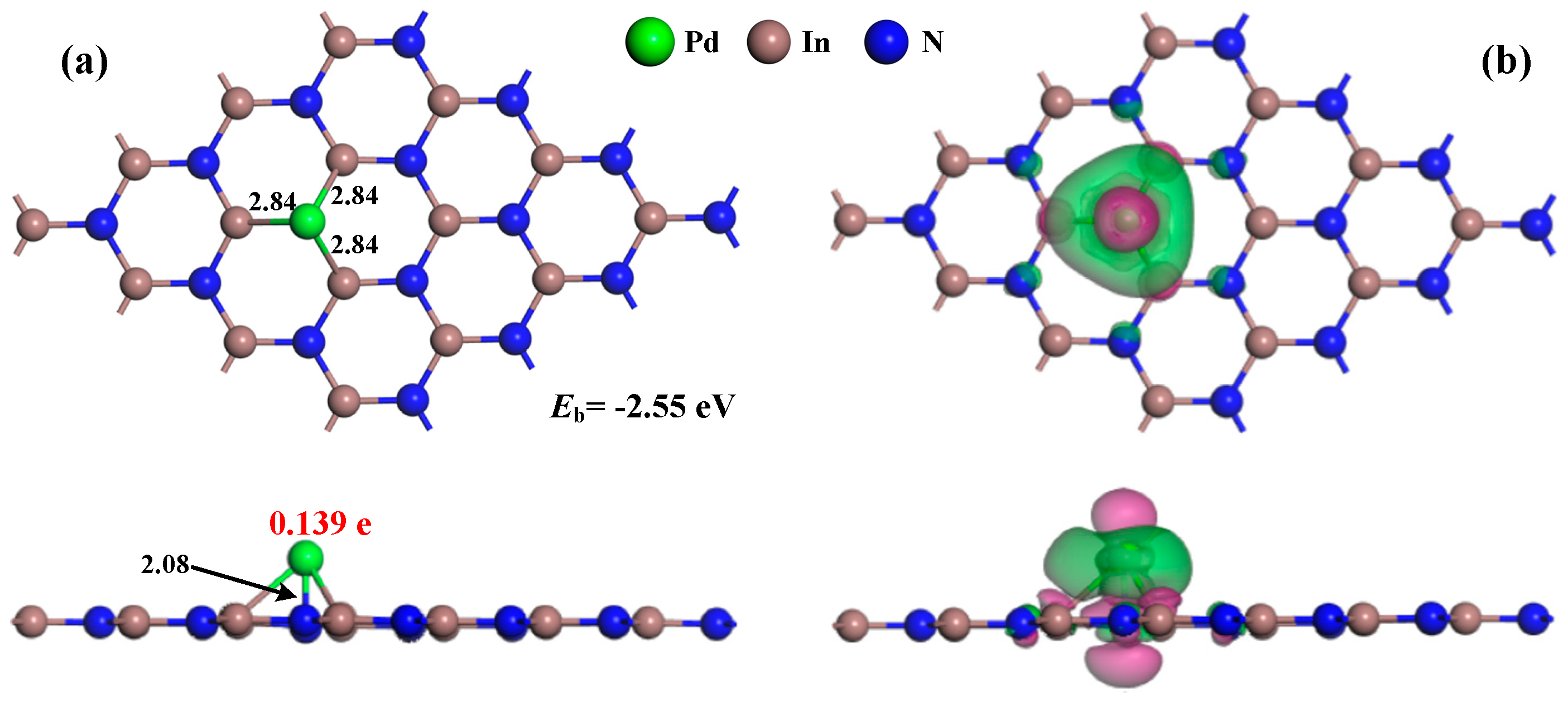
3.1. Analysis of Pd-InN Monolayer

For Pd-doping on the InN monolayer, four possible sites have been recognized, namely TB (the bridge site on the top of the In-N bond), TH (in the hollow center of the hexatomic In-N ring), TN (on the top of the N atom), and TIn (on the top of the In atom). As reported in Reference [17], Pd prefers to be doped on the TN site, with the binding energy of −2.47 eV. Thus, in this work, we directly employed the TN site for Pd-doping on the intrinsic InN monolayer, with a calculated binding energy (Eb) of −2.55 eV.
The geometric structure associated with the deformation charge density (EDD) of our optimized Pd-InN monolayer is shown in Figure 1. According to our calculations, the bandgap obtained by the PBE function (0.606) is much closer to the previous report (0.62 eV [16]) than the HSE06 function (0.670 eV). Thus, in the following calculations, we employed the PBE functional to discuss the properties. One can see from Figure 1a that the Pd dopant captured on the right top of the N atom is bonded with it and three neighboring In atoms of the InN monolayer. The new formed Pd-N and Pd-In bonds were measured as 2.08 and 2.84 Å, respectively. After doping, the Pd atom was positively charged by 0.139 e, which indicated its electron-donating property transferring charge to the InN surface. As shown in Figure 1b, it was found that, in the Pd dopant, three bonded In atoms were encompassed with electron depletion, while the N atom under the Pd dopant were somewhat surrounded by electron accumulation. Thus, there is no wonder that strong electron accumulation is localized on the Pd-In and Pd-N bonds that account for their formation. These findings imply the electron-transfer from the Pd dopant to the InN layer and the remarkable electron hybridization on the Pd-In and Pd-N bonds.
Figure 2 depicts the density of state (DOS) distribution of the Pd-InN system. As can be seen in Figure 2a, several novel peaks appeared that around −3, −1, and 2.5 eV in the Pd-doped surface, compared with the total DOS of the intrinsic InN counterpart. This could be attributed to the introduction of the Pd atom on the InN surface., which induces several impurity states around the Fermi level. As a consequence of this, the DOS peaks in the Pd-InN monolayer below the Fermi level, where the Pd dopant contributes remarkably, are dramatically increased. From Figure 2b, one can find that the state contributions of the Pd dopant are mainly from its 4d orbital, which behaves actively and hybridizes strongly with the N 2p and In 5p orbitals of the bonding atoms. One can see that the hybridization between the Pd 4d orbital and the In 5p orbital is much stronger than that with N 2p, indicating the stronger binding force of Pd-In bonds. This is in agreement with the larger electron accumulation on the Pd-In bonds, which verifies the stable adsorption of Pd dopant on the InN monolayer with the formation of chemical bonds. In addition, from the atomic DOS, we could also conclude that the top of the valence band is mainly localized on the Pd atom and the bottom of the conduction band is mainly on the In atoms [31], which supports the electron-donating behavior of the Pd dopant.

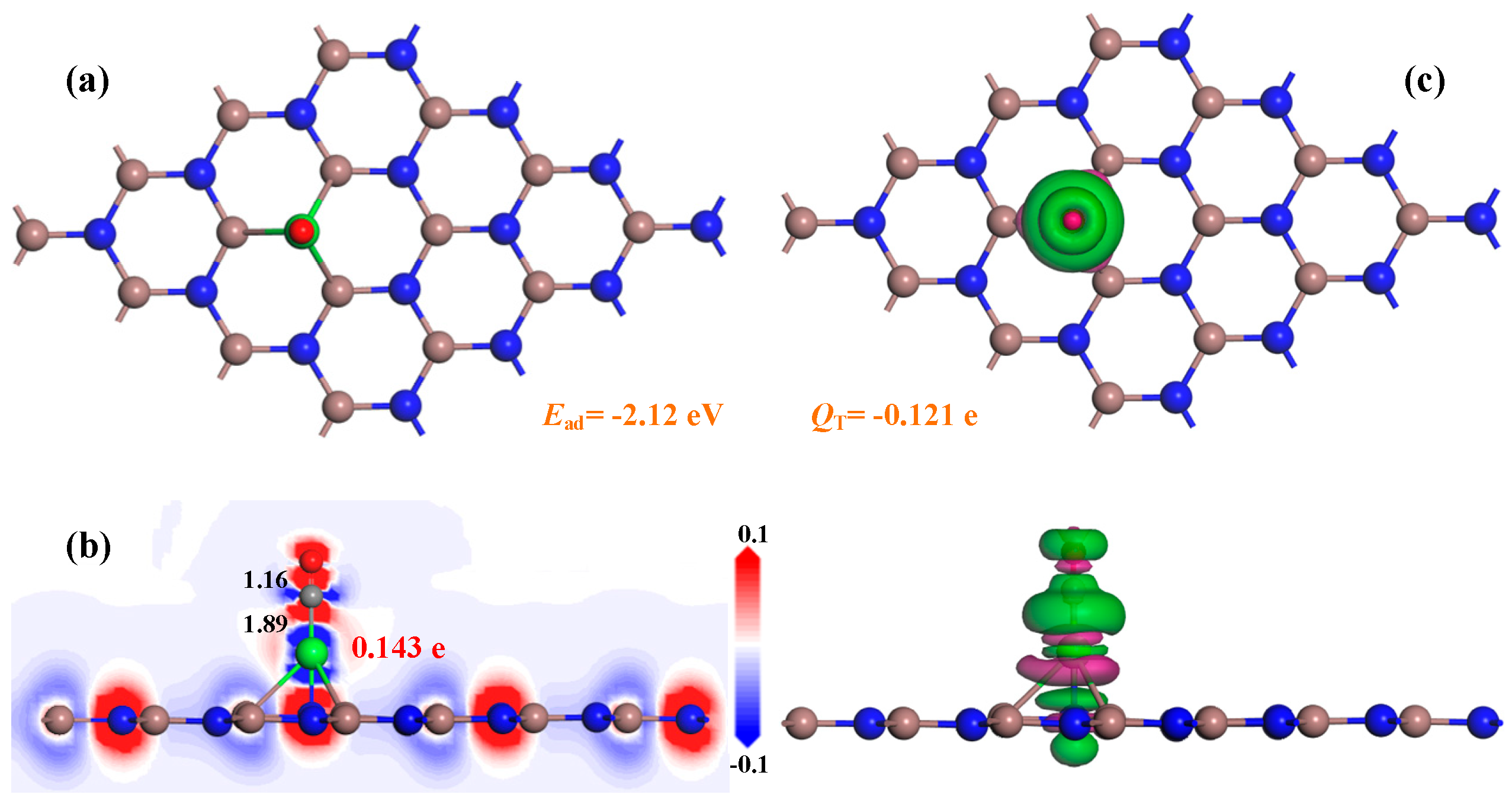
3.2. Adsorption Behavior of the Pd-InN Monolayer

With the relaxed Pd-InN monolayer, we implemented the adsorption of CO and NO molecules onto the surface and plotted the most stable configurations in Figure 3 and Figure 4, respectively, in which the electron localization function (ELF) is also depicted to display the bonding behavior in the adsorbed systems.
As can be seen in Figure 3a, in the CO system the CO molecule was vertically adsorbed on the top of the Pd dopant by the C-end position, forming the Pd-C bond (shown in Figure 3b) measured at 1.89 Å. At the same time, the C≡O bond on the inner of the CO molecule elongated to 1.16 Å from 1.14 Å for the gas phase, while the Pd-N and Pd-In bonds were prolonged to 2.09 and 3.01 Å, respectively. These deformations indicate the activation effect on the geometries of the CO molecule and the Pd-InN monolayer during adsorption [32]. The calculated Ead for CO adsorption is −2.12 eV, much larger than that in a pristine InN system (−0.223 eV), as reported in Reference [15], indicating the enhanced adsorption performance of Pd-doping on the nano-surface. After adsorption, the CO molecule accepts 0.121 e from the Pd-InN surface, in which the Pd dopant loses 0.004 e, which indicates that Pd behaves as a media bridging the charge-transfer from the InN layer to the CO molecule. Such an amount of charge-transfer (0.117 e) is larger than that in a pristine InN system as well, confirming the enhancement in surface reactivity of the InN monolayer after Pd-doping. The electron hybridization between Pd and C atoms according to the dense electron accumulation and depletion on the Pd-C bond is visible in Figure 3b. From Figure 3c, where the EDD is shown, we can observe strong electron accumulation on the CO molecule and electron depletion on the Pd dopant, which is in line with the Hirshfeld method. Apart from that, electron depletion appears on the Pd-In and Pd-N bonds, suggesting their weakened binding force, which accords with their elongation.
When it comes to the NO system, as shown in Figure 4a, the most stable configuration for NO adsorption is same as that for CO adsorption. The N atom was oriented to the Pd dopant, forming a new Pd-N bond of 1.86 Å, as displayed in Figure 4b. Meanwhile, the C=O bond elongated to 1.17 Å from 1.16 Å for the isolated molecule, while in the Pd-InN monolayer the Pd-N bond shortened to 2.05 Å after adsorption. This may attribute to the predominant protrusion of the N atom in the InN layer. Along with such deformation, the Pd-In bonds were broken as well. However, the electron hybridization between the Pd dopant and the N atom of the NO molecule remained quite strong, as seen in ELF. The Ead (−1.65 eV) and QT (−0.093) in the NO system were not as large as those in CO system, indicating the relatively weak interaction here, but it was still larger than that in the pristine InN system (−0.380 eV) [15]. Based on the Hirshfeld method, the NO molecule performed an electron-accepting property, but the Pd dopant contributed most of the charge-transfer (0.061 e) to the gas species. Thus, we assume that the binding force of Pd-N for NO adsorption will be stronger than that of Pd-C for CO adsorption. The electron accumulation on NO molecule and the electron depletion on Pd dopant are not as strong as that in CO system, in agreement with the Hirshfeld analysis, as shown in Figure 4c. Moreover, the electron hybridization on the Pd-N bond could be found given the overlap between the electron accumulation and the electron depletion.
Additionally, we performed the zero-point vibrational energy (ZPVE) correction to calculate Ead in the CO and NO systems. The ZPVE of the Pd-InN monolayer, the gas molecules, and the adsorbed systems are listed in Table 1. Based on these results, the ZPVE correction in the CO and NO systems would be 0.08 and 0.03 eV, and the Ead with ZPVE correction were obtained as −2.04 and −1.62 eV, respectively. In this regard, we assume that the adsorption is chemically stable with little difference in Ead when the temperature is extrapolated to 0 K.
In short, the Pd-InN monolayer has admirable adsorption behavior upon CO and NO molecules. On the basis of the calculated Ead in two systems, chemisorption can be identified [33]. This assumption could be further confirmed by the bond length analysis. According to the previous report [34], the covalent bond length of Pd-C and Pd-N are 1.95 and 1.91 Å, respectively. That is, the new-formed Pd-C and Pd-N bonds in the adsorbing systems are much shorter than their covalent bond length, suggesting their strong binding force and their chemical bond nature. Furthermore, it is worth noting that the larger electron hybridization between Pd and gaseous species can lead to more discrepancy in the conductivity of the Pd-InN monolayer [35,36], which would be beneficial for a resistance-type gas sensor. In order to further verify the electronic behavior of Pd-InN upon CO and NO adsorption, DOS and band structure analysis was performed and is described in the next section.

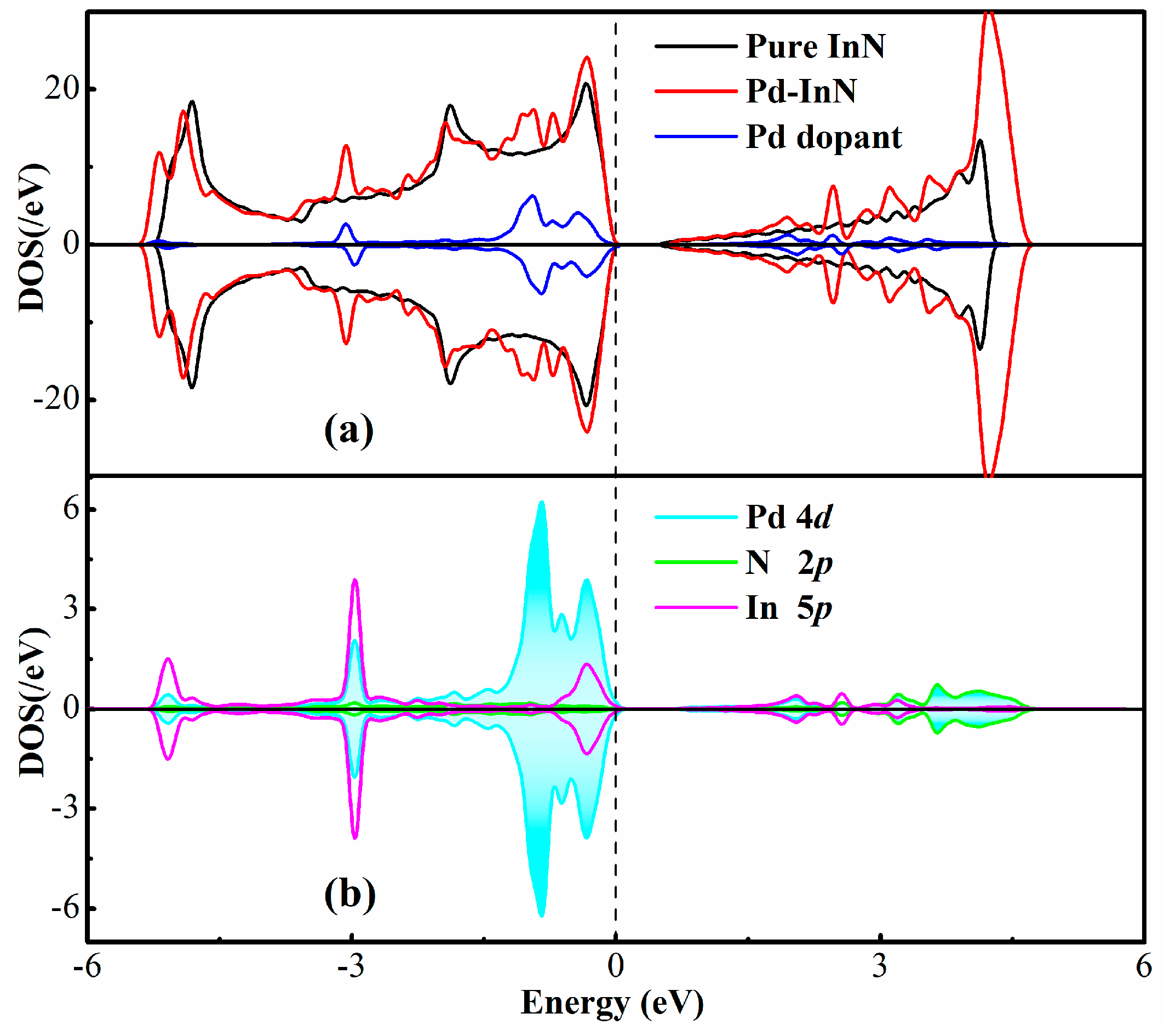
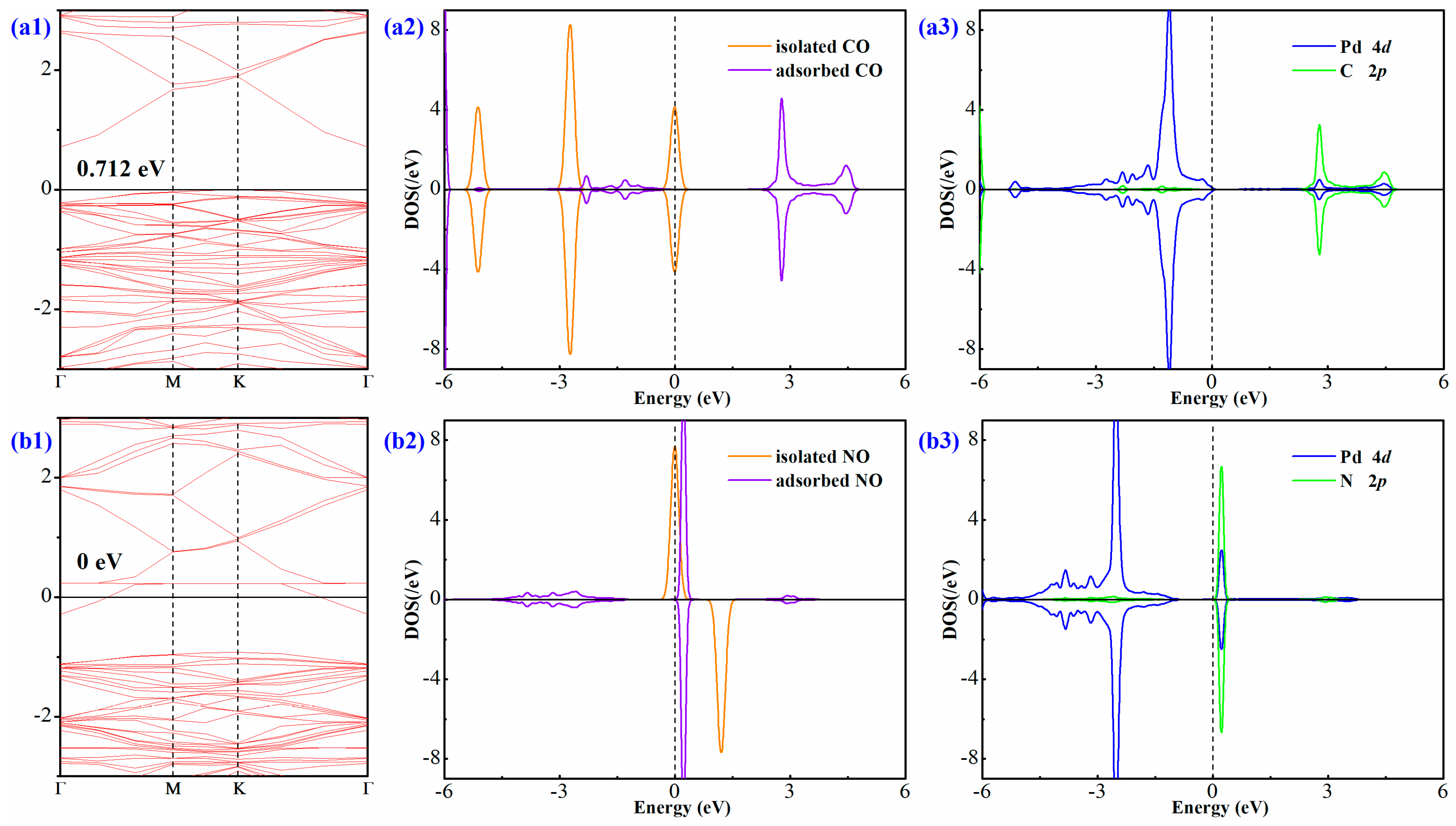
3.3. Electronic Behavior of Pd-InN upon Gas Adsorption

Figure 5 presents the band structures of gas adsorption systems, the molecular DOS of target gases, and the atomic DOS of bonded atoms. Based on our calculations, the bandgap of the Pd-InN monolayer was obtained as 0.748 eV. In the CO system, the band gap was slightly narrowed to 0.712 eV, which attributes the electron redistribution caused by the charge-transfer [37] from the Pd-InN monolayer to the CO molecule. The charge-transfer could activate the orbitals of the CO molecule [38], making the DOS deform accordingly. It could be found that the states at −5, −2.8, and 0 eV in isolated CO molecular DOS disappeared, while several small peaks around −3–0 and 3 eV in adsorbed CO molecular DOS emerged, which suggests the activation of molecular orbitals in adsorption. Moreover, the electron hybridization during charge-transfer can support the activation of molecular orbitals as well [39], and it therefore could account for the change in the electronic behavior of the whole system. One can see that there are somewhat hybridization between Pd 4d and C 2p orbitals around −3–0 and 3 eV, which verifies the formation of chemical bonds due to the orbital interaction [40,41].
Upon the NO system, from the band structure, we can see that there was one state at the top of the conduction band crossing the Fermi level, forming an n-doping behavior for the Pd-InN monolayer [42]. Accordingly, the system behaved semimetallic in property and the bandgap was calculated as 0 eV. In the molecular DOS, the deformations not only included the disappeared magnetic moment of the NO molecule, but also laid in the shift of states after adsorption. Particularly, the state at the Fermi level became unoccupied and altered to the region above the Fermi level. Moreover, the N 2p orbital of this activated NO state was highly hybrid with the Pd 4d orbital in adsorption, verifying the chemical bond of Pd-N given the strong electron hybridization. The stronger binding force of Pd-N in the NO system than in the Pd-C in CO system could also be verified due to the larger overlapped area. In other words, the change of the electronic behavior of the Pd-InN monolayer in the NO system was more significant than that in CO system, which could result in a larger change in conductivity in the former system. For sensing applications, the Pd-InN monolayer may be more admirable for NO detection.

3.4. Application of the Pd-InN Monolayer

A band gap of a typical surface can be obtained through band structure calculations and it is a workable parameter to evaluate the electrical conductivity of the related material [43]. Therefore, the change in the band gap of the Pd-InN monolayer after gas adsorption indicated the increase or reduction of its resistance in the presence of specific gases. A wide band gap corresponds to a large conductivity and a narrow band gap corresponds to a small conductivity [44,45], which expounds the basic sensing mechanism of the Pd-InN monolayer as a resistance-type gas sensor. The detailed relationship between band gap and conductivity is calculated as σ = A e ( B g / 2 k T ) [46,47], where A is the certain constant, Bg is the bandgap, k is Boltzmann constant, and T is the working temperature. Based on these, it is believed that the Pd-InN monolayer has a dramatic electrical response upon NO, given the semimetallic property after gas adsorption, while a small change in conductivity would be obtained in the CO system, due to the slight change in electronic behavior of the Pd-InN monolayer in the existence of the CO molecule. However, considering the strong adsorption performance of the Pd-InN monolayer upon CO, it could be proposed as a CO adsorbent for the removal of such toxic gases in certain environments. We assume that this would be a promising application for the Pd-doped surface as well [48].
In short, the Pd-InN monolayer could be a promising candidate as a resistance-type sensor for NO detection and as a gas adsorbent for CO removal. We are hopeful that this work can offer the basic physicochemical properties and potential applications of the Pd-InN monolayer, which is beneficial for its further exploration in many fields.

4. Conclusions

Using first-principles theory, we theoretically investigated the physicochemical properties of a Pd-InN monolayer that are associated with its adsorption behavior upon CO and NO molecules. ELF and electron EDD, as well as DOS, were considered to comprehensively understand the electronic properties of the proposed surface before and after gas adsorption. For the geometric and electronic behavior of the Pd-InN monolayer, our calculations are in good agreement with the previous report. Upon CO and NO adsorption, it was found that the Pd-InN monolayer has a better adsorption performance upon CO molecules, but has more remarkable change in the electronic behavior in a NO system. Our results indicate that the Pd-InN monolayer could be a promising candidate as a resistance-type sensor for NO detection and as a gas adsorbent for CO removal. Our work is meaningful for provide some guidance for the further exploration of the Pd-InN monolayer.

Author Contributions

S.Z. analyzed the data and S.M. guided this work and wrote this paper.

Funding

This research received no external funding.

Conflicts of Interest

The authors declare no conflict of interest.

References

  1. Pierucci, D.; Zribi, J.; Henck, H.; Chaste, J.; Silly, M.G.; Bertran, F.; Le Fèvre, P.; Gil, B.; Summerfield, A.; Beton, P.H.; et al. Van der Waals epitaxy of two-dimensional single-layer h-BN on graphite by molecular beam epitaxy: Electronic properties and band structure. Appl. Phys. Lett. 2018, 112, 253102. [Google Scholar] [CrossRef]
  2. Cui, H.; Chen, D.; Zhang, Y.; Zhang, X. Dissolved gas analysis in transformer oil using Pd catalyst decorated MoSe2 monolayer: A first-principles theory. Sustain. Mater. Technol. 2019, 20, e00094. [Google Scholar] [CrossRef]
  3. Comini, E.; Baratto, C.; Faglia, G.; Ferroni, M.; Vomiero, A.; Sberveglieri, G. Quasi-one dimensional metal oxide semiconductors: Preparation, characterization and application as chemical sensors. Prog. Mater. Sci. 2009, 54, 1–67. [Google Scholar] [CrossRef]
  4. Cui, H.; Chen, D.; Yan, C.; Zhang, Y.; Zhang, X. Repairing the N-vacancy in an InN monolayer using NO molecules: A first-principles study. Nanoscale Adv. 2019, 1, 2003–2008. [Google Scholar] [CrossRef]
  5. Hashimoto, A.; Suenaga, K.; Gloter, A.; Urita, K.; Iijima, S. Direct evidence for atomic defects in graphene layers. Nature 2004, 430, 870–873. [Google Scholar] [CrossRef] [PubMed]
  6. Xu, M.; Liang, T.; Shi, M.; Chen, H. Graphene-Like Two-Dimensional Materials. Chem. Rev. 2013, 113, 3766–3798. [Google Scholar] [CrossRef] [PubMed]
  7. Krishnan, R.; Su, W.S.; Chen, H.T. A new carbon allotrope: Penta-graphene as a metal-free catalyst for CO oxidation. Carbon 2017, 114, 465–472. [Google Scholar] [CrossRef]
  8. Sun, Z.; Chang, H. Graphene and Graphene-like Two-Dimensional Materials in Photodetection: Mechanisms and Methodology. ACS Nano 2014, 8, 4133–4156. [Google Scholar] [CrossRef]
  9. Cui, H.; Zhang, X.; Li, Y.; Chen, D.; Zhang, Y. First-principles insight into Ni-doped InN monolayer as a noxious gases scavenger. Appl. Surf. Sci. 2019, 494, 859–866. [Google Scholar] [CrossRef]
  10. Sarmazdeh, M.M.; Mendi, R.T.; Zelati, A.; Boochani, A.; Nofeli, F. First-principles study of optical properties of InN nanosheet. Int. J. Mod. Phys. B 2016, 30, 1650117. [Google Scholar] [CrossRef]
  11. dos Santos, R.B.; Mota, F.B.; Rivelino, R.A.; Kakanakova-Georgieva, G.; Gueorguiev, K. Van der Waals stacks of few-layer h-AlN with graphene: An ab initio study of structural, interaction and electronic properties. Nanotechnology 2016, 27, 145601. [Google Scholar] [CrossRef] [PubMed]
  12. Caliskan, S.; Hazar, F. First principles study on the spin unrestricted electronic structure properties of transition metal doped InN nanoribbons. Superlattices Microstruct. 2015, 84, 170–180. [Google Scholar] [CrossRef]
  13. Maleyre, B.; Briot, O.; Ruffenach, S.; Gil, B. Optical investigations on Si-doped InN films. Phys. Status Solidi 2010, 2, 1379–1383. [Google Scholar] [CrossRef]
  14. Yu, K.M.; Liliental-Weber, Z.; Walukiewicz, W.; Shan, W.; Ager, J.W.; Li, S.X.; Jones, R.E.; Haller, E.E.; Lu, H.; Schaff, W.J. On the crystalline structure, stoichiometry and band gap of InN thin films. Appl. Phys. Lett. 2005, 86, 071910. [Google Scholar] [CrossRef]
  15. Sun, X.; Yang, Q.; Meng, R.; Tan, C.; Liang, Q.; Jiang, J.; Ye, H.; Chen, X. Adsorption of gas molecules on graphene-like InN monolayer: A first-principle study. Appl. Surf. Sci. 2017, 404, 291–299. [Google Scholar] [CrossRef]
  16. Chen, D.; Zhang, X.; Tang, J.; Cui, Z.; Cui, H. Pristine and Cu decorated hexagonal InN monolayer, a promising candidate to detect and scavenge SF6 decompositions based on first-principle study. J. Hazard. Mater. 2019, 363, 346–357. [Google Scholar] [CrossRef] [PubMed]
  17. Guo, Y.H.; Zhang, Y.M.; Wu, W.X.; Liu, Y.X.; Zhou, Z.P. Transition metal (Pd, Pt, Ag, Au) decorated InN monolayer and their adsorption properties towards NO2: Density functional theory study. Appl. Surf. Sci. 2018, 455, 106–114. [Google Scholar] [CrossRef]
  18. Cui, H.; Zhang, X.X.; Chen, D.C.; Tang, J. Pt & Pd decorated CNT as a workable media for SOF2 sensing: A DFT study. Appl. Surf. Sci. 2019, 471, 335–341. [Google Scholar]
  19. Cui, H.; Zhang, X.; Zhang, J.; Mehmood, M.A. Interaction of CO and CH4 Adsorption with Noble Metal (Rh, Pd, and Pt)-Decorated N3-CNTs: A First-Principles Study. ACS Omega 2018, 3, 16892–16898. [Google Scholar] [CrossRef] [Green Version]
  20. Cui, H.; Zhang, G.; Zhang, X.; Tang, J. Rh-doped MoSe2 as a toxic gas scavenger: A first-principles study. Nanoscale Adv. 2019, 1, 772–780. [Google Scholar] [CrossRef]
  21. Li, K.J.; Wang, W.C.; Cao, D.P. Metal (Pd, Pt)-decorated carbon nanotubes for CO and NO sensing. Sens. Actuators B Chem. 2011, 159, 171–177. [Google Scholar] [CrossRef]
  22. Ma, D.W.; Ju, W.W.; Li, T.X.; Zhang, X.W.; He, C.Z.; Ma, B.Y.; Lu, Z.S.; Yang, Z.X. The adsorption of CO and NO on the MoS2 monolayer doped with Au, Pt, Pd, or Ni: A first-principles study. Appl. Surf. Sci. 2016, 383, 98–105. [Google Scholar] [CrossRef]
  23. Delley, B. From molecules to solids with the DMol 3 approach. J. Chem. Phys. 2000, 113, 7756–7764. [Google Scholar] [CrossRef]
  24. Cui, H.; Qiu, G.; Wang, J.; Li, Q. Carbon-chain inserting effect on electronic behavior of single-walled carbon nanotubes: A density functional theory study. MRS Commun. 2018, 8, 189–193. [Google Scholar] [CrossRef]
  25. Tamijani, A.A.; Salam, A.; De Lara-Castells, M.P. Adsorption of Noble-Gas Atoms on the TiO2 (110) Surface: An Ab Initio-Assisted Study with van der Waals-Corrected DFT. J. Phys. Chem. C 2016, 120, 18126–18139. [Google Scholar] [CrossRef]
  26. Grimme, S. Semiempirical GGA-type density functional constructed with a long-range dispersion correction. J. Comput. Chem. 2006, 27, 1787–1799. [Google Scholar] [CrossRef]
  27. Cui, H.; Liu, T.; Zhang, Y.; Zhang, X. Ru-InN Monolayer as a Gas Scavenger to Guard the Operation Status of SF6 Insulation Devices: A First-Principles Theory. IEEE Sens. J. 2019, 19, 5249–5255. [Google Scholar] [CrossRef]
  28. Cui, H.; Zhang, X.; Chen, D.; Tang, J. Adsorption mechanism of SF6 decomposed species on pyridine-like PtN3 embedded CNT: A DFT study. Appl. Surf. Sci. 2018, 447, 594–598. [Google Scholar] [CrossRef]
  29. Monkhorst, H.J.; Pack, J.D. Special points for Brillouin-zone integrations. Phys. Rev. B 1976, 13, 5188–5192. [Google Scholar] [CrossRef]
  30. Saoud, F.S.; Plenet, J.C.; Henini, M. Structural, electronic and vibrational properties of InN under high pressure. Phys. B Condens. Matter 2012, 407, 1008–1013. [Google Scholar] [CrossRef] [Green Version]
  31. Cui, H.; Zhang, X.S.; Zhang, J.; Tang, J. Adsorption behaviour of SF6 decomposed species onto Pd4-decorated single-walled CNT: A DFT study. Mol. Phys. 2018, 116, 1749–1755. [Google Scholar] [CrossRef]
  32. Fan, Y.; Zhang, J.; Qiu, Y.; Zhu, J.; Zhang, Y.; Hu, G. A DFT study of transition metal (Fe, Co, Ni, Cu, Ag, Au, Rh, Pd, Pt and Ir)-embedded monolayer MoS 2 for gas adsorption. Comput. Mater. Sci. 2017, 138, 255–266. [Google Scholar] [CrossRef]
  33. Cui, H.; Zhang, X.X.; Chen, D.C. Borophene: A promising adsorbent material with strong ability and capacity for SO2 adsorption. Appl. Phys. A 2018, 124, 636. [Google Scholar] [CrossRef]
  34. Pyykko, P.; Atsumi, M. Molecular Single-Bond Covalent Radii for Elements 1-118. Chem. A Eur. J. 2009, 15, 186–197. [Google Scholar] [CrossRef]
  35. Wu, P.; Yin, N.; Li, P.; Cheng, W.; Huang, M. The adsorption and diffusion behavior of noble metal adatoms (Pd, Pt, Cu, Ag and Au) on a MoS 2 monolayer: A first-principles study. Phys. Chem. Chem. Phys. 2017, 19, 20713–20722. [Google Scholar] [CrossRef] [PubMed]
  36. Giovanni, M.; Poh, H.L.; Ambrosi, A.; Zhao, G.; Sofer, Z.; Šaněk, F.; Khezri, B.; Webster, R.D.; Pumera, M. Noble metal (Pd, Ru, Rh, Pt, Au, Ag) doped graphene hybrids for electrocatalysis. Nanoscale 2012, 4, 5002–5008. [Google Scholar] [CrossRef] [PubMed]
  37. Lu, Z.; Lv, P.; Ma, D.; Yang, X.; Li, S.; Yang, Z. Detection of gas molecules on single Mn adatom adsorbed graphyne: A DFT-D study. J. Phys. D Appl. Phys. 2018, 51, 065109. [Google Scholar] [CrossRef]
  38. Zhang, D.; Jiang, C.; Wu, J.; Junfeng, W. Layer-by-layer assembled In2O3 nanocubes/flower-like MoS2 nanofilm for room temperature formaldehyde sensing. Sens. Actuators B Chem. 2018, 273, 176–184. [Google Scholar] [CrossRef]
  39. Baek, D.H.; Kim, J. MoS2 gas sensor functionalized by Pd for the detection of hydrogen. Sens. Actuators B Chem. 2017, 250, 686–691. [Google Scholar] [CrossRef]
  40. Ju, W.; Li, T.; Su, X.; Li, H.; Li, X.; Ma, D. Au cluster adsorption on perfect and defective MoS2 monolayers: Structural and electronic properties. Phys. Chem. Chem. Phys. 2017, 19, 20735–20748. [Google Scholar] [CrossRef]
  41. Zhao, B.; Li, C.; Liu, L.; Zhou, B.; Zhang, Q.; Chen, Z.; Tang, Z. Adsorption of gas molecules on Cu impurities embedded monolayer MoS2: A first- principles study. Appl. Surf. Sci. 2016, 382, 280–287. [Google Scholar] [CrossRef]
  42. Ma, D.W.; Wang, Q.G.; Li, T.X.; He, C.Z.; Ma, B.Y.; Tang, Y.N.; Lu, Z.S.; Yang, Z.X. Repairing sulfur vacancies in the MoS2 monolayer by using CO, NO and NO2 molecules. J. Mater. Chem. C 2016, 4, 7093–7101. [Google Scholar] [CrossRef]
  43. Xia, C.; Peng, Y.; Zhang, H.; Wang, T.; Wei, S.; Jia, Y. The characteristics of n- and p-type dopants in SnS2 monolayer nanosheets. Phys. Chem. Chem. Phys. 2014, 16, 19674. [Google Scholar] [CrossRef] [PubMed]
  44. Cui, H.; Zhang, X.; Yao, Q.; Miao, Y.; Tang, J. Rh-doped carbon nanotubes as a superior media for the adsorption of O2 and O3 molecules: A density functional theory study. Carbon Lett. 2018, 28, 55–59. [Google Scholar]
  45. Cui, H.; Zhang, X.; Zhang, G.; Tang, J. Pd-doped MoS2 monolayer: A promising candidate for DGA in transformer oil based on DFT method. Appl. Surf. Sci. 2019, 470, 1035–1042. [Google Scholar] [CrossRef]
  46. Semiconductor Physical Electronics; Springer: New York, NY, USA, 2006; Volume 28, pp. 363–364.
  47. Zhang, X.; Yu, L.; Wu, X.; Hu, W. Experimental Sensing and Density Functional Theory Study of H2S and SOF2 Adsorption on Au-Modified Graphene. Adv. Sci. 2015, 2, 1500101. [Google Scholar] [CrossRef] [PubMed]
  48. Su, Y.T.; Ao, Z.M.; Ji, Y.M.; Li, G.Y.; An, T.C. Adsorption mechanisms of different volatile organic compounds onto pristine C2N and Al-doped C2N monolayer: A DFT investigation. Appl. Surf. Sci. 2018, 450, 484–491. [Google Scholar] [CrossRef]
Figure 1. Configuration (a) and EDD (b) of the Pd-InN monolayer. The black values are bond lengths while the red value is the charge of the Pd dopant. In EDD, the green and rosy regions represent electron accumulation and depletion, respectively. The isosurface is set to 0.005 eV/Å3.
Applsci 09 03390 g001
Figure 2. Total DOS (a) and partial DOS (b) of Pd-InN. The dash line is the Fermi level.
Applsci 09 03390 g002
Figure 3. The most stable configuration (a), ELF (b) and EDD (c) for CO adsorption on the Pd-InN monolayer. The setting in EDD is same as Figure 2. The black values are bond length while the red value is the charge of the Pd dopant.
Applsci 09 03390 g003
Figure 4. The most stable configuration (a), ELF (b) and EDD (c) for NO adsorption on the Pd-InN monolayer. Other settings are same as Figure 3.
Applsci 09 03390 g004
Figure 5. Band structures and DOS distributions of adsorbing systems. (a1a3) CO system; (b1b3) NO system. The figures from left to right successively represent band structures of gas adsorption systems, the molecular DOS of target gases, and the atomic DOS of bonded atoms. The dash line is the Fermi level.
Applsci 09 03390 g005
Table 1. ZPVE of Pd-InN monolayer, gas molecules and adsorbed systems.
SystemPd-InNCO MoleculeNO MoleculePd-InN/COPd-InN/NO
ZPVE (eV)1.910.130.122.112.06

