Article

Multi-Variable Thermal Modeling of Power Devices Considering Mutual Coupling

1
Collaborative Innovation Center of Electric Vehicles in Beijing, National Engineering Laboratory for Electric Vehicles, School of Mechanical Engineering, Beijing Institute of Technology, Beijing 100081, China
2
Faculty of Engineering and Information Technology, University of Technology Sydney, Sydney, NSW 2007, Australia
*
Author to whom correspondence should be addressed.
Appl. Sci. 2019, 9(16), 3240; https://doi.org/10.3390/app9163240
Submission received: 10 July 2019 / Revised: 6 August 2019 / Accepted: 7 August 2019 / Published: 8 August 2019
(This article belongs to the Section Electrical, Electronics and Communications Engineering)

Abstract

:
In relation to power converter design, power density is increasing while the form factor is decreasing. This trend generally reduces the rate of the cooling process, which increases the mutual thermal coupling among the surrounding power components. Most of the traditional models usually ignore the mutual effects or just focus on the conduction coupling. To deal with these factors, the thermal modeling for a boost converter system has been built to compare the junction temperatures (Tj) and the increments under different working conditions in order to consider the conduction coupling. A multi-variable thermal resistances model is proposed in this paper to incorporate the convection thermal coupling into the mutual thermal effects. The coupling resistances, MOSFET to the diode ( R cp- MD ), and the diode to MOSFET ( R cp- DM ) have been calculated and the relationships between coupling resistances and their impact factors (separation distances and working currents) have been discussed. New case temperatures (Tc) obtained by calculation and additional measurements at other separation distances serve to verify the efficacy of the proposed model. This model enhances the current thermal models and provides an effective method to calculate the thermal coupling resistances which can be used to estimate the Tj. As the coupling resistances are distance dependent, the model also helps to optimize and fine-tune the placements of components in high-power density converters.

1. Introduction

For industrial applications, reliability and power density are two important considerations in the design process of power converters. Modern power converters with increased power density require efficient and intelligent thermal design and management [1,2] to ensure the reliability of the systems. Accordingly, there is an ongoing need to build thermal models to help thermal analysis and power converter optimization.
The forth-order Foster [3,4] and Cauer networks [5,6] are being widely used to describe the thermal response of junction-to-case for power components. Based on the Cauer network, the one-dimensional thermal network can be extended to one or two orders of case-to-heatsink as shown in Figure 1 [7] for thermal analysis. The network is fast to calculate the junction temperatures (Tj) of power components. While this kind of model just focuses on the self-resistances, it cannot calculate the thermal coupling.
In a compact IGBT (insulated-gate bipolar transistor) module, multiple IGBT chips and diodes are packaged as shown in Figure 2a. Tj of the Si-chips can be affected thermally by the neighboring chips placed on the same substrate. Based on the multi-chip structure of an IGBT module, the networks built in [8,9] consider the conduction thermal coupling resistance (Rcdcp) generated by neighboring Si-chips. The model in Figure 2b can be used to calculate the Tj of power devices and the method is more accurate than the ones that do not consider the effect of thermal coupling among the surrounding chips. While this kind of thermal model just focuses on a single module, it ignores the coupling between modules in a system.
FEM simulations [10] can be used to describe the thermal distribution of components or converter systems and the junction and case temperatures can be extracted by adding virtual thermal probes to active and passive power components. The thermal coupling matrix in [11] is extracted by FEM simulation with a given power to heat up the chip. In this study Rcdcp is dependent on the geometric positions of the chips in a LED module. This thermal matrix is used for Tj estimation. Heat flow in Figure 3 shows the Rcdcp that is generated among several structure layers and the model in [12] compares the temperatures at the same position in the vertical direction of each layer and computes the thermal resistances among them. However, to build more accurate FEM models, familiarity with complex geometric structures, appropriate meshing methods, and boundary conditions are essential [13]. This model focuses on the coupling between different layers in a single module and it does not consider the coupling between neighboring modules.
Erik et al. built a thermal model which considers the Rcdcp between the components in a power converter based on the surface or case temperatures (Tc) mapping in [14]. The Rcdcp in the red color in Figure 4 are generated by connected copper traces in the PCB and these resistances are dependent on the location of the components. Their locations can be optimized based on the temperature’s mapping network and a power converter is optimized in [15]. The advantage of this model is that it considers the components in the overall system. While this model just focuses on the conduction coupling, it ignores the convection coupling effect.
Higher power and smaller size are required for high-power density converters [16,17], which make the process of thermal dissipation more difficult. Moreover, power devices are exposed in power converters and part of the heat that is released in the narrow space by the way of convection and thermal convection is environmentally dependent. Changes of convection coupling will be induced when the thermal environment is changed in the converters. Due to these factors, thermal convection cannot be ignored [18], and the thermal models should incorporate the convection thermal coupling resistances (Rcvcp) among the heating components. These thermal models in the literature ignore the effect of convection coupling [19]. Furthermore, the method is not extensively discussed and analyzed for the purposes of calculating the thermal coupling resistances (Rcp) which include Rcdcp and Rcvcp.
The major contributions of this paper are as follows: thermal analysis of a boost converter system has been given to compare the junction temperatures and the increments under different working conditions; a multi-variable thermal analysis resistances network has been built which includes Rcdcp and Rcvcp; the coupling resistances, MOSFET to the diode ( R cp- MD ) and the diode to MOSFET ( R cp- DM ), have been respectively calculated based on the proposed model; and the relationships between Rcp and their impact factors (separation distances and working currents) have been discussed.
The paper is organized as follows: First, the thermal analysis of a boost converter is given in Section 2. Measurement of thermal coupling of power components and losses calculation are presented in Section 3. A multi-variable thermal resistances model has been established in Section 4. Calculation and coupling measurements at new separation distances have been built to verify the proposed model in Section 5. Finally, the main conclusion is drawn in Section 6.

2. Thermal Models in a Boost Converter System

There are two important considerations in the converter design phase to ensure the reliable operation of the converter: (1) Maximum junction temperature Tj of the devices, e.g., Si-based devices, cannot exceed 175 °C [1,20]; and (2) the ability to share heat among the components with a much greater uniform temperature distribution [14,21]. Figure 5 describes three cases of thermal maps, where Figure 5c shows the best thermal profile for converter design and operation. This means it is desirable to control the temperatures at junctions in order to operate the power devices at good temperature ranges within the safety operation region even in the worst-case scenario. Thermal coupling resistances analysis among the components can help with the thermal distribution.
In a DC-DC boost converter, the MOSFET and the diode are two key heating components which can affect the performance of the overall converter systems [22]. PLECS has its advantages to simulate the dynamic systems for power converters [23]. The simulation schematics are shown in Figure 6. These figures give basic thermal models which are used for thermal descriptions and the Tj increments’ ( Δ T j ) comparisons.
The thermal model simulates the boost converter at different frequencies (10 kHz, 20 kHz, and 50 kHz) and different loading resistances (5 Ω, 8 Ω, and 10 Ω). Figure 7 gives the Δ T j at different frequencies (load: 5 Ω) for the MOSFET (duty cycle: 0.5) and the diode with a shared heatsink (System 1) and two separate heatsinks (System 2), respectively. Figure 8 gives the Δ T j at different loads (frequency: 20 kHz). The load voltage, load current, and inductor current under different working conditions are also given in Figure 7 and Figure 8.
Based on the simulation results, the value of Δ T j increases while the frequency increases which indicates a greater thermal coupling effect at a higher frequency. The value of Δ T j decreases with the smaller operating current (by increasing loading resistance). In other words, the greater thermal coupling effect will be induced by a larger current passing through the MOSFET and the diode, and vice versa. Moreover, the Tj of the MOSFET and the diode with a shared heatsink are relatively higher than the ones with separate single heatsinks. The major reason for causing these is the conduction thermal coupling between the two devices, since they share the same heatsink. However, these kinds of models cannot calculate the convection coupling.

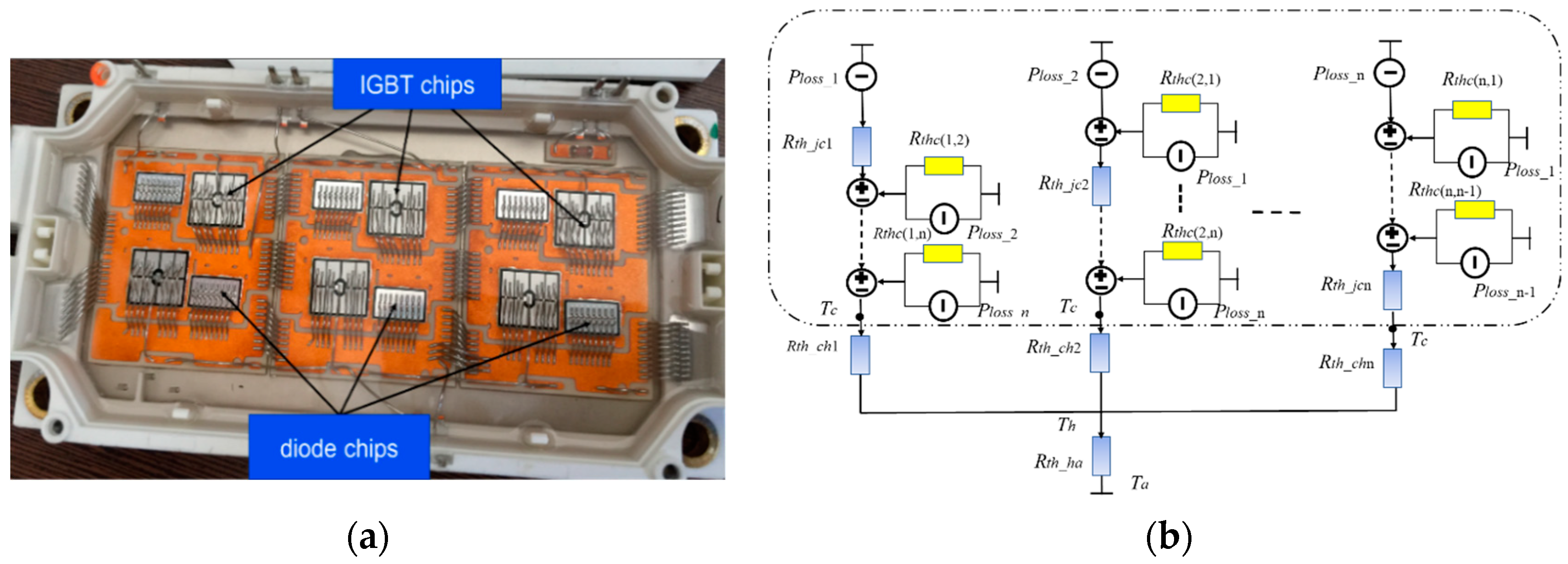
3. Thermal Coupling of Power Components

The convection coupling effect is not easily calculated under different working conditions because of the environmental dependency. In this section, the thermal coupling platform is established to analyze the mutual coupling which includes the conduction and convection thermal coupling.

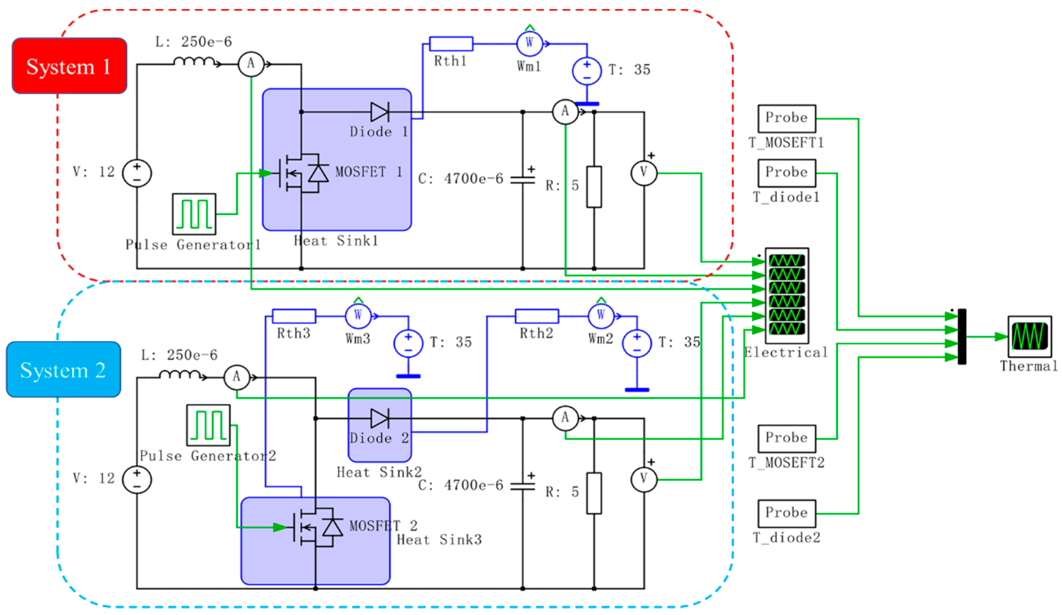
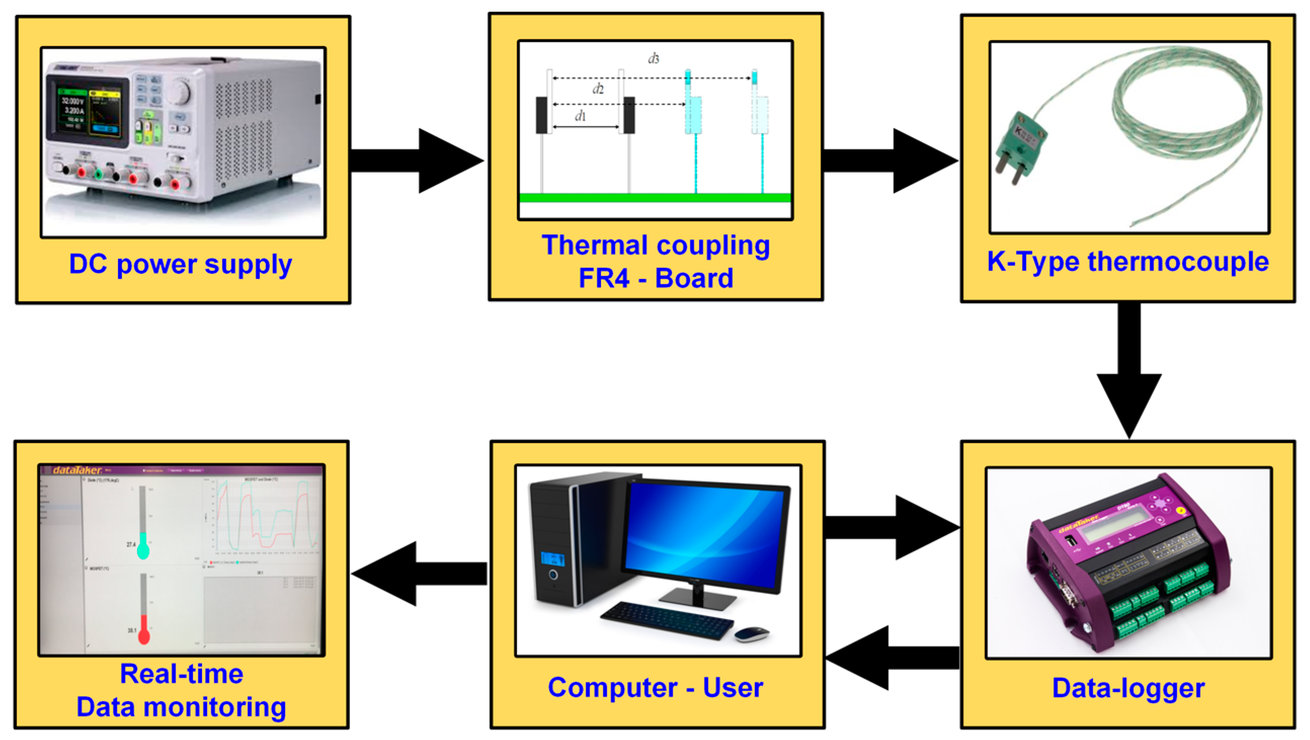
3.1. The Experimental Platform

The thermal coupling platform is illustrated in Figure 9. This experimental platform includes: one 30 V DC power supply for the MOSFET gate driving, a controlled DC current supply for the testing circuit (5 A), two power components (MOSFET: IRF540NPBF, Infineon, Munich, Bavaria, Germany, and diode: MBR20100CT, ON Semiconductor, Phoenix, Arizona, USA) packaged with TO-220, a digital multimeter which is used for observing the voltage-drop of the diode, a current sensor which is used to measure the current levels, a data Taker Data Logger (DT80 with eight bi-directional channels, Thermo Fisher Scientific, Waltham, MA, USA) which is employed for collecting the measurement data, K-type thermocouples attached to the case of the devices for Tc testing [24,25], and real-time data monitoring by a computer and a FR4 PCB board.
In power converter applications when the MOSFET and the diode are working, power losses (the conduction loss and switching loss, etc.) will be generated and all the power losses will become factors of component heating. Therefore, a given power loss [11] or controlled currents [26] can heat up the devices. In this study, we focus on the on-state mode and after the devices have undergone conduction loss, thermal dissipation will ensue.
The two power devices are measured in the thermal coupling experimental platform with the distances of 12 mm, 18 mm, and 22 mm and under three different working currents, respectively. In one minute, 30 Tc values (a maximum of 600 data can be collected) for the MOSFET and the diode are collected by a Data-Taker and for every testing current it takes 20 min at the separation distances, as shown in Figure 10. When the devices are powered on, Tc increases at a fast rate and then reaches its steady state. Since the diode has a higher power loss than the MOSFET, it has a faster rate of increase and a higher steady temperature. When the devices are powered off, Tc decreases at a considerable rate and then reaches Ta and the diode also decreases at a faster rate than the MOSFET. All measured Tc data in steady state, Tc-M for the MOSFET and Tc-D for the diode, are shown in Table 1.

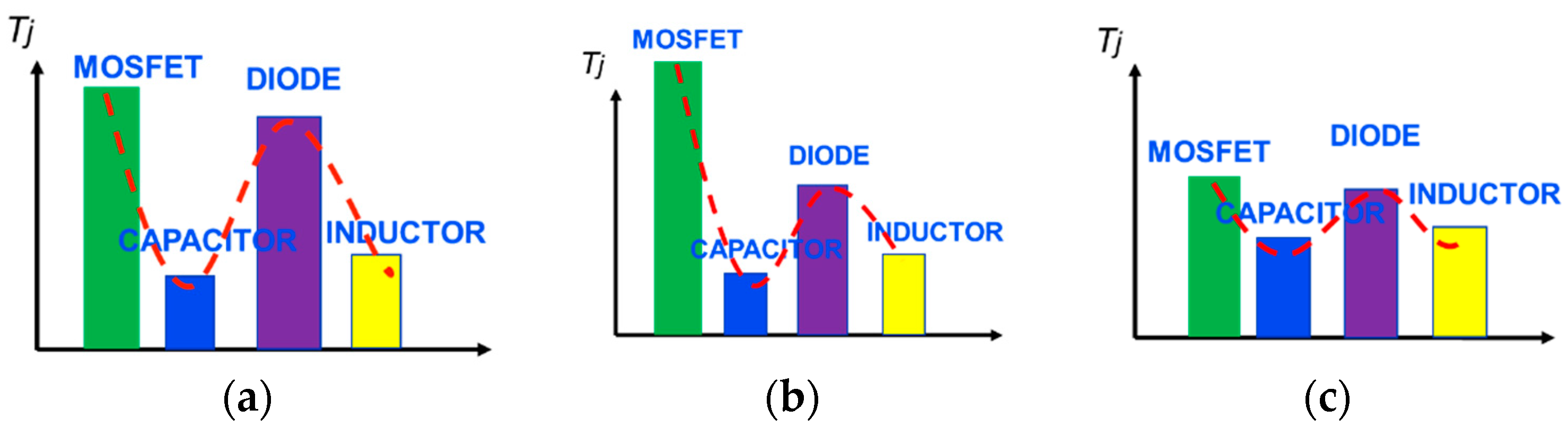
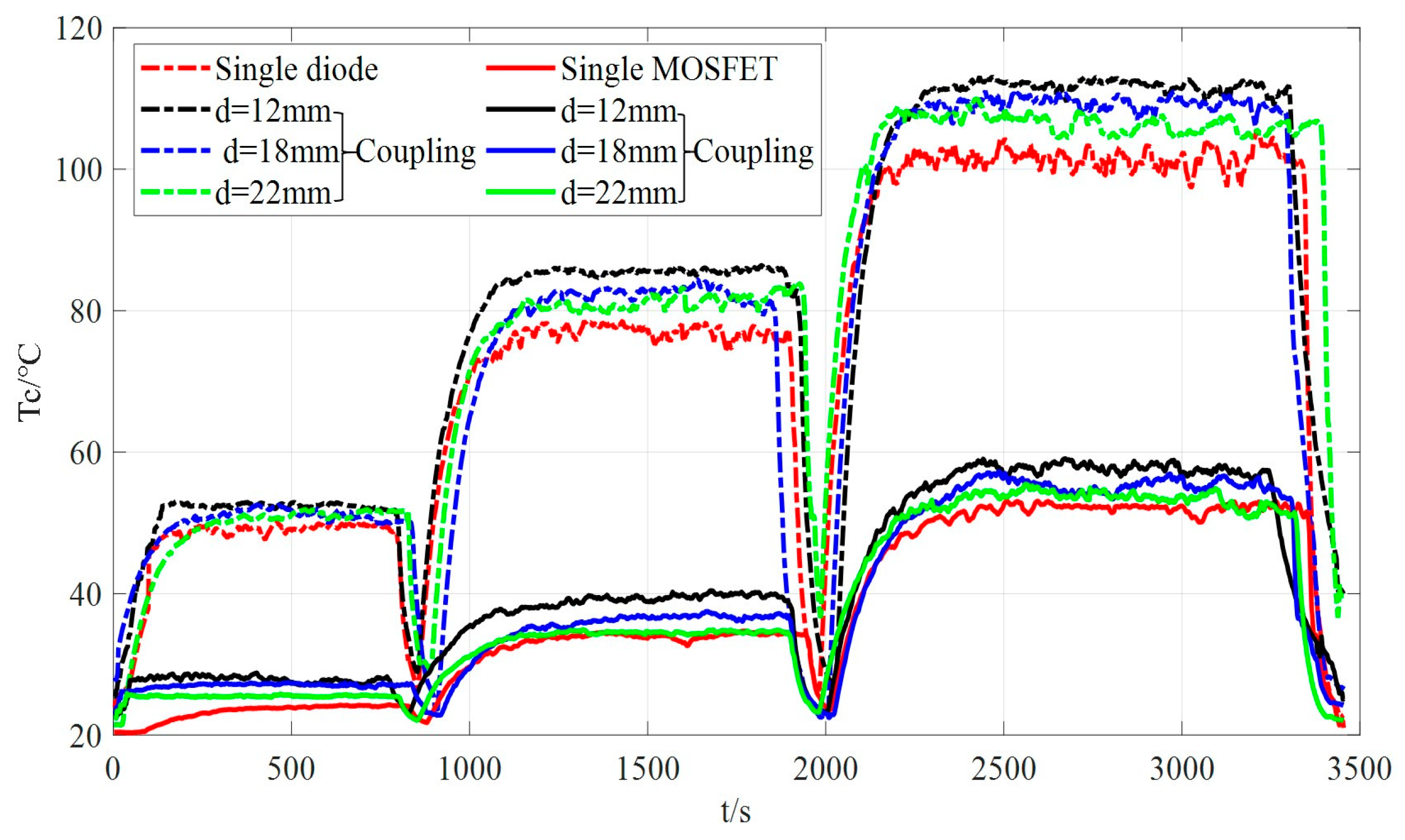
3.2. Losses Calculation and Tc Comparisons

Power losses are regarded as the main cause of heat generation through power semiconductor devices. In the testing process, power components are in the on-state, and the conduction losses contribute to the temperature increments for the MOSFET and the diode [27,28]. The losses for the MOSFET (PM) and the diode (PD) can be computed by [29]:
{   P M   =   R D   S I 2 P D   =   V f d   I
where RDS is the on-state resistance for the MOSFET [24]. The value is 44 mΩ for the MOSFET (IRF540N) at ambient temperature (Ta) and the relationship between RDS and Tj is given in the datasheet [30]. Vfd is the forward voltage drop of the diode which can be collected by a digital multimeter in the steady-state and I is the working current.
Figure 11 gives the comparisons of Tc between single device testing and thermal coupling testing at different separation distances between the power devices and different working currents. When the devices are individually tested, Tc in the steady state is lowest and when the devices are mutually tested, Tc for the MOSFET and the diode display increasing trends and the Tc increases in size with the reduction of the separation distances.

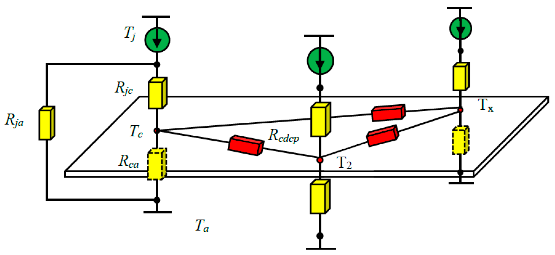
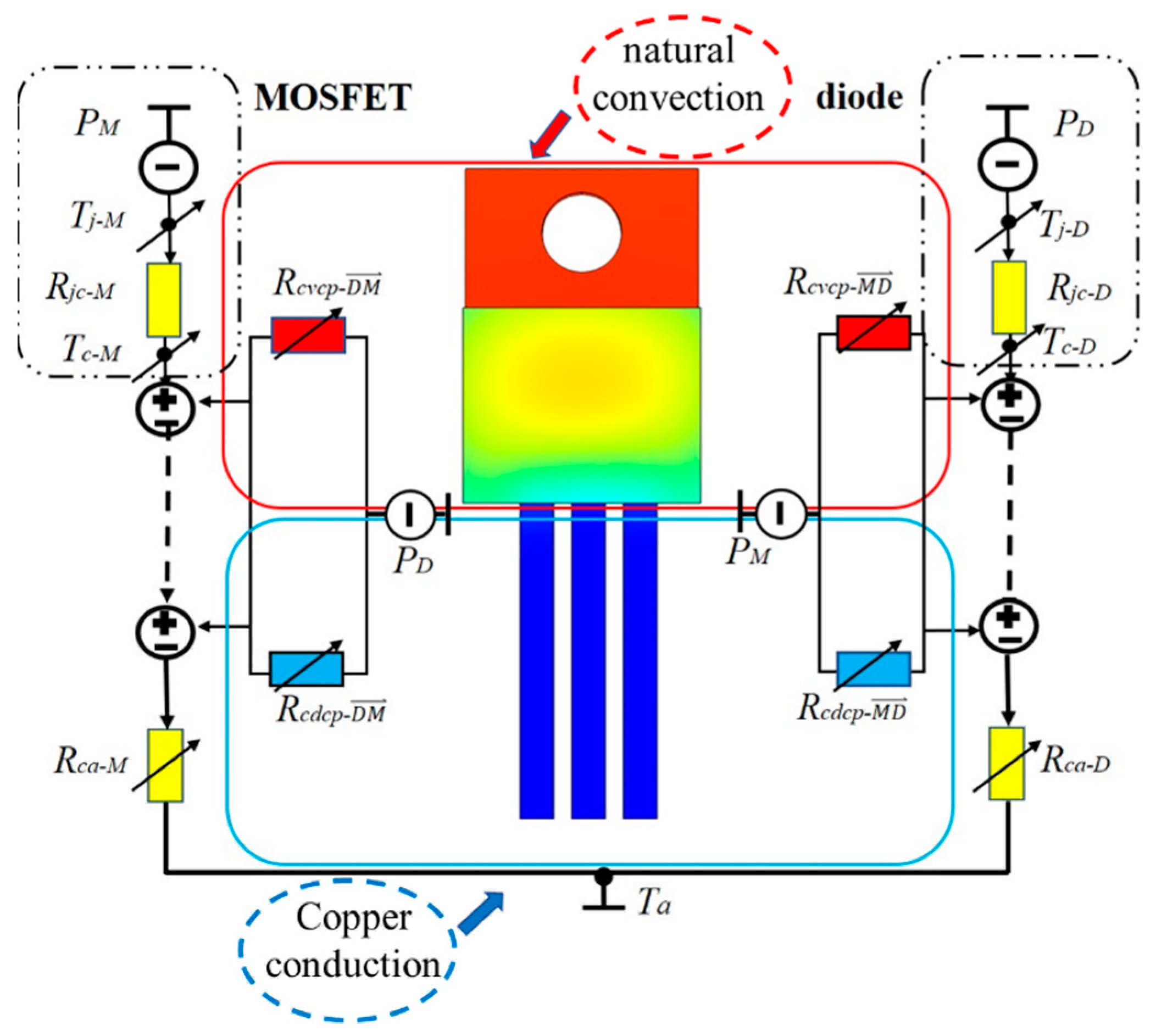
4. Multi-Variable Thermal Resistances Network Modeling

4.1. Thermal Resistances Network

For thermal analysis of these power components, which are realized in the experimental results, it should be noted that the values of Tj, Tc, and all the thermal resistances are variable when the separation distances and the working currents change. Then a multi-variable thermal resistances model is established considering the self-resistances [31] and coupling resistances between the power components. Based on the analysis of the traditional thermal models in the literature section, the models always ignore the mutual thermal effects or only focus on the Rcdcp. In this paper, the Rcvcp has been added into the multi-variable thermal network and in this new network the variable thermal resistances are as follows: (1) the self-resistances: junction-to-case resistance (Rjc); case-to-ambient resistance (Rca); and (2) the thermal coupling resistances (Rcp), Rcdcp, which is given through the device pins connected via copper traces; and Rcvcp, which is given through the air between the two power components. The power losses for the MOSFET and the diode (PM and PD) are the heat sources in the network. The packages for the devices are supposed to be insulated and all the heat is released from case and fins and the air domain is considered as an incompressible fluid [32,33,34]. During the process of heat distribution, mutual thermal coupling will affect the Tj and Tc for the power devices. The thermal analysis model can be given as shown in Figure 12.

4.2. Self-Resistances Calculation

Rjc is in the process of thermal conduction which can be obtained from the datasheet. The method to calculate Rca in the steady state is given as:
R ca   =   T c   T a P
Therefore, Rca for the MOSFET and the diode can be obtained by:
{ R ca-M   =   T c-M     T a P M R ca-D   =   T c-D   T a P D
Putting the experimental data into Equation (3), the values of Rca-M and Rca-D in different working conditions can be calculated, as shown in Table 2.

4.3. Thermal Coupling Resistances Calculation

Rcdcp can be calculated based on the method in [14]:
R cdcp   = l   λ   A
where l is the length of copper traces, λ is the thermal conductivity, and A is the cross-sectional area.
According to the proposed thermal coupling resistances network, Rcp is the result of Rcdcp and Rcvcp in parallel and can be given as Equation (5), respectively.
{ R cp- MD   =   1 1 R cdcp- MD   +   1 R cvcp MD R cp- DM   =   1 1 R cdcp DM   + 1   R cvcp DM
where R cp- MD is the thermal coupling resistance of MOSFET to the diode and R cp- DM is the coupling resistance of the diode to the MOSFET.
Based on [12], Rcp in the steady state can be calculated by:
{ R cp- MD   =   | T c-M     T c-D | P M R cp- DM   =   | T c-D     T c-M | P D
If we bring all the measured Tc data from Table 1 into Equation (6), the values of R cp- MD and R cp- DM at different separation distances and different currents can be calculated and given in Table 3.

4.4. Relationships

Table 3 shows that the separation distances between power components and working currents are the two key impact factors for thermal coupling resistances R cp- MD and R cp- DM . The relationships between them can be described as Equation (7) and Figure 13 gives the relationships based on data curve fitting:
{ R cp- MD   =   f   ( d   ,   I   ) R cp- DM   =   g   ( d   ,   I   )
The relationships between thermal coupling resistances and their impact factors, d and I, are detailed in Table 4 and summarized as follows.
(1)
The values of R cp- MD and R cp- DM increase when the distance between power components increases, which means the coupling effect decreases when the separation distances increase, and vice versa.
(2)
The values of R cp- MD and R cp- DM decrease when the working currents increase, which means the coupling effect increases when the currents increase, and vice versa.
(3)
R cp- MD and R cp- DM have decreasing trends when the currents increase and the distances decrease, which means the coupling effect increases when the devices are brought closer with higher current magnitude, and vice versa.

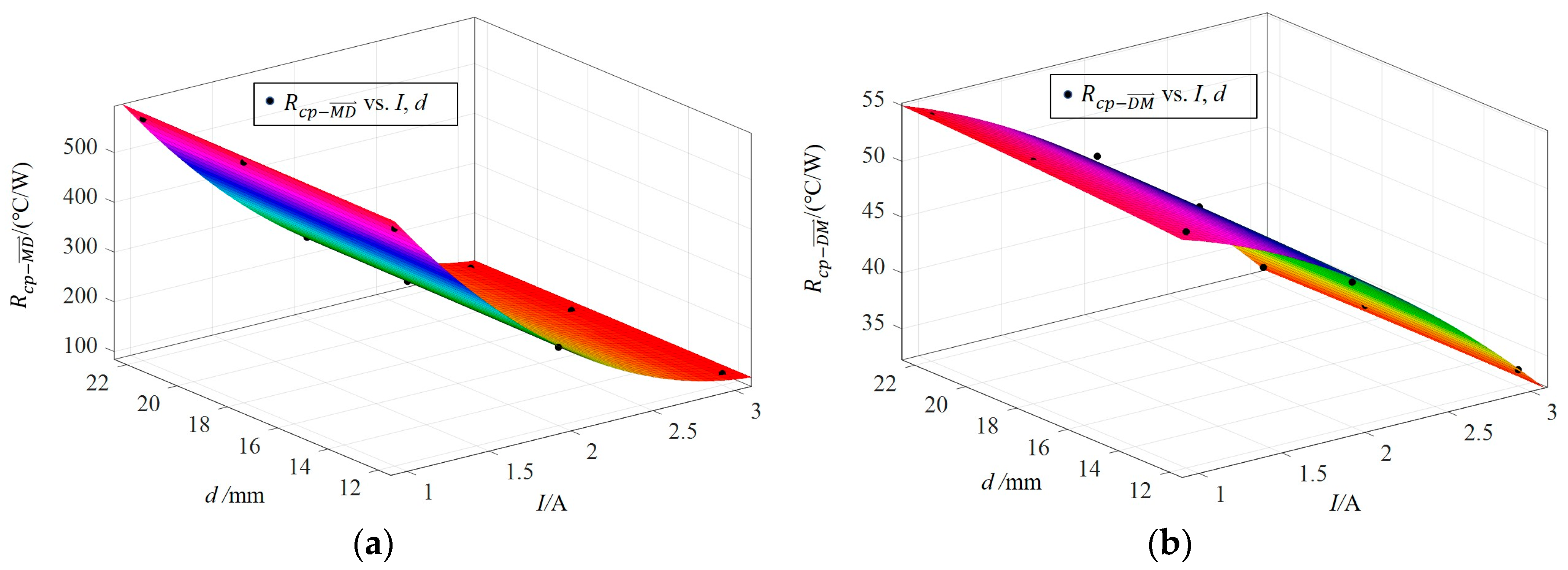
4.5. Rcp Calculation
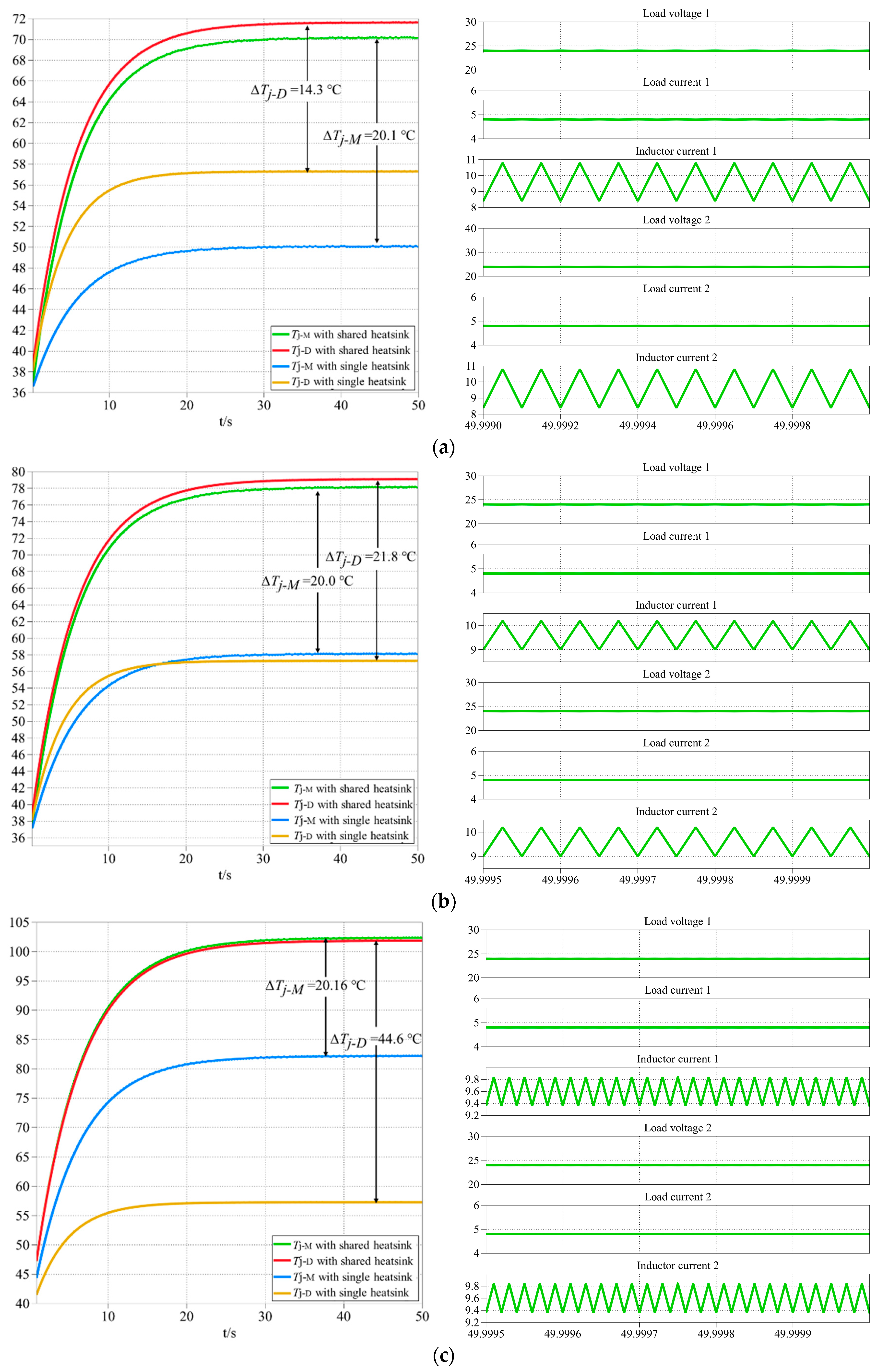
Based on Figure 13, the formula for calculating Rcp considering different distances and currents can be given in Equation (8) and the Rcp in other separation distances (12 mm ≤ d ≤ 22 mm) or working currents (1 A ≤ I ≤ 3 A) can be estimated by this method:
{ R cp- MD   =   A -M   +   B -M I   +   C -M d   +   E -M I   2 +   F -M I d   +   G -M d 2 R cp- DM   =   A -D   +   B -D I   +   C -D d   +   E -D I 2   +   F -D I d   +   G -D d 2
where:
{ A -M   =   1040 B -M   =   584.6 C -M   =   1.79 E -M   =   90.55 F -M   =   0.409 G -M   =   0.012 ,   and   { A -D   =   52.32 B -D   =   0.47 C -D   =   0.34 E -D   =   2.40 F -D   =   0.058 G -D   =   0.005

5. Verifications

To verify the proposed multi-variable thermal resistances model, the coupling resistances have been calculated by Equation (8) and more measurements with d = 15 mm, I = 1 A, 2 A, and 3 A have been taken. The comparisons of calculation and measurements are shown in Table 5 for R cp- MD and Table 6 for R cp- DM , respectively. Like the relationships discussed in Section 4.4, the values of R cp- MD and R cp- DM have decreasing trends when the working currents increase, and all the errors are less than 4%.

6. Conclusions

In this study, comparisons of junction temperatures and the increments in a boost converter system have been given to show the conduction thermal coupling effect under different working conditions. Conduction and convection coupling have been added into the mutual thermal effects and a multi-variable thermal resistances model has been built, which includes the variable thermal resistances,   R cp- MD and R cp- DM . In addition, the relationships between the thermal coupling resistances and their impact factors (d and I) have been discussed. Calculation and measurements have been done to verify the concept. The errors between the calculations and measurements are less than 4% for both the MOSFET and the diode, which prove the efficacy of the proposed method. Based on the proposed thermal model, Tj can be estimated. Moreover, heatsinks can be included by adding the thermal resistances of heatsinks to discuss the cooling schemes. Additionally, extension thermal models can be given for the overall converters by adding thermal resistances of other components (e.g., capacitors, inductors) to assist the components layouts and the separation distances between them in order to optimize the power converters.

Author Contributions

K.W. wrote the manuscript and performed the experiment. Thermal analysis was carried out by K.W. and T.C., Y.P.S. implemented the simulation and modified the manuscript, D.D.-C.L. and C.Z. designed and supported the experiment.

Funding

This research was funded partially by the National Natural Science Foundation of China (grant number: 51677005), and partially by the Australian Government through the Australian Research Council (Discovery Project No. DP180100129).

Acknowledgments

This research would like to thank UTS (University of Technology Sydney) and BIT (Beijing Institute of Technology) Collaborative Doctoral Research Degree Program.

Conflicts of Interest

The authors declare no conflict of interest.

References

  1. Gautam, D.; Wager, D.; Musavi, F.; Edington, M.; Eberle, W.; Dunford, W.G. A review of thermal management in power converters with thermal vias. In Proceedings of the 2013 Twenty-Eighth Annual IEEE Applied Power Electronics Conference and Exposition (APEC), Long Beach, CA, USA, 17–21 March 2013. [Google Scholar]
  2. Hasan, A.; Hejase, H.; Abdelbaqi, S.; Assi, A.; Hamdan, M. Comparative effectiveness of different phase change materials to improve cooling performance of heat sinks for electronic devices. Appl. Sci. 2016, 6, 226. [Google Scholar] [CrossRef]
  3. Natarajan, S.; Ha, M.; Graham, S. Measuring the thermal resistance in light emitting diodes using a transient thermal analysis technique. IEEE Trans. Electron Devices 2013, 60, 2548–2555. [Google Scholar] [CrossRef]
  4. Wei, K.; Wang, W.; Hu, Z.; Du, M. Condition Monitoring of IGBT Modules Based on Changes of Thermal Characteristics. IEEE Access 2019, 7, 47525–47534. [Google Scholar] [CrossRef]
  5. Hanini, W.; Ayadi, M. Electro thermal modeling of the power diode using Pspice. Microelectron. Reliab. 2018, 86, 82–91. [Google Scholar] [CrossRef]
  6. Davidson, J.; Stone, D.; Foster, M. Required Cauer network order for Modeling of thermal transfer impedance. Electron. Lett. 2014, 50, 260–262. [Google Scholar] [CrossRef]
  7. Luo, Z.; Ahn, H.; Nokali, M. A thermal model for insulated gate bipolar transistor module. IEEE Trans. Power Electron. 2004, 19, 902–907. [Google Scholar] [CrossRef]
  8. Li, H.; Liao, X.; Zeng, Z.; Hu, Y.; Li, Y.; Liu, S.; Ran, L. Thermal Coupling Analysis in a Multichip Paralleled IGBT Module for a DFIG Wind Turbine Power Converter. IEEE Trans. Energy Convers. 2017, 32, 80–90. [Google Scholar] [CrossRef]
  9. Reichl, J.; Ortiz-Rodriguez, J.M.; Hefner, A.; Lai, J.S. 3-D thermal component model for electrothermal analysis of multichip power modules with experimental validation. IEEE Trans. Power Electron. 2015, 30, 3300–3308. [Google Scholar] [CrossRef]
  10. Bernardoni, M.; Cova, P.; Delmonte, N.; Menozzi, R. Heat management for power converters in sealed enclosures: A numerical study. Microelectron. Reliab. 2009, 49, 1293–1298. [Google Scholar] [CrossRef]
  11. Lu, H.L.; Lu, Y.J.; Zhu, L.H.; Lin, Y.; Guo, Z.Q.; Liu, T.; Chen, Z. Efficient measurement of thermal coupling effects on multichip light-emitting diodes. IEEE Trans. Power Electron. 2017, 32, 9280–9292. [Google Scholar] [CrossRef]
  12. Bahman, S.A.; Ma, K.; Blaabjerg, F. A Lumped Thermal Model Including Thermal Coupling and Thermal Boundary Conditions for High-Power IGBT Modules. IEEE Trans. Power Electron. 2018, 33, 2518–2530. [Google Scholar] [CrossRef]
  13. Pepper, D. The Intermediate Finite Element Method: Fluid Flow and Heat Transfer Applications; Routledge: Abingdon-on-Thames, UK; London, UK, 2017. [Google Scholar]
  14. De Jong, W.C.E.; Ferreira, J.A.; Bauer, P. Thermal design based on surface temperature mapping. IEEE Power Electron. Lett. 2005, 3, 125–129. [Google Scholar] [CrossRef]
  15. De Jong, W.C.E.; Ferreira, J.A.; Bauer, P. Design techniques for thermal management in switch mode converters. IEEE Trans. Ind. Appl. 2006, 42, 1375–1386. [Google Scholar] [CrossRef]
  16. Marz, M. Thermal management in high-density power converters. IEEE Int. Conf. Ind. Technol. 2003, 2, 1196–1201. [Google Scholar]
  17. Wanes, J. A novel integrated packaging technique for high density DC-DC converters providing enhanced efficiency and thermal management. In Proceedings of the Nineteenth Annual IEEE Applied Power Electronics Conference and Exposition, Anaheim, CA, USA, 22–26 February 2004. [Google Scholar]
  18. Haque, S.; Xing, K.; Suchicital, C.; Nelson, D.J.; Lu, G.Q.; Borojevic, D.; Lee, F.C. Thermal management of high-power electronics modules packaged with interconnected parallel plates. Fourteenth Annu. IEEE Semicond. Therm. Meas. Manag. Symp. 1998, 1195, 111–119. [Google Scholar]
  19. Vermeersch, B.; De Mey, G. Dependency of thermal spreading resistance on convective heat transfer coefficient. Microelectron. Reliab. 2008, 48, 734–738. [Google Scholar] [CrossRef]
  20. Laloya, E.; Lucia, O.; Sarnago, H.; Burdio, J.M. Heat management in power converters: From state of the art to future ultrahigh efficiency systems. IEEE Trans. Power Electron. 2016, 31, 7896–7908. [Google Scholar] [CrossRef]
  21. De Jong, W.C.E.; Ferreira, B.J.; Bauer, P. Toward the next level of PCB usage in power electronic converters. IEEE Trans. Power Electron. 2008, 23, 3151–3163. [Google Scholar] [CrossRef]
  22. Bulut, Y.; Pandya, K. Thermal modeling for power MOSFETs in DC/DC applications. In Proceedings of the 5th International Conference on Thermal and Mechanical Simulation and Experiments in Microelectronics and Microsystems, Brussels, Belgium, 10–12 May 2004. [Google Scholar]
  23. Biweta, M.; Mamo, M. Closed loop control strategy of back to back PWM converter fed by PMSG using PLECS toolbox on Matlab/Simulink for wind energy application. In Proceedings of the 2017 IEEE AFRICON, Cape Town, South Africa, 18–20 September 2017. [Google Scholar]
  24. Lai, W.; Zhao, Y.; Chen, M.; Wang, Y.; Ding, X.; Xu, S.; Pan, L. Condition Monitoring in a Power Module Using On-State Resistance and Case Temperature. IEEE Access 2018, 6, 67108–67117. [Google Scholar] [CrossRef]
  25. Rodriguez, R.; Alizadeh, M.; Bauman, J.; Ravi, P.S.; Emadi, A. Performance Evaluation of Thermal Management for a 3-Phase Interleaved DC-DC Boost Converter. In Proceedings of the 2018 IEEE Transportation Electrification Conference and Expo (ITEC), Long Beach, CA, USA, 13–15 June 2018. [Google Scholar]
  26. Kulkarni, A.; John, V. Thermal model for paralleled surface-mount power MOSFETs. In Proceedings of the 2014 IEEE International Conference on Power Electronics, Drives and Energy Systems (PEDES), Mumbai, India, 16–19 December 2014. [Google Scholar]
  27. Kim, T.; Jang, M.; Agelidis, V.G. Practical implementation of a silicon carbide-based 300 kHz, 1.2 kW hard-switching boost-converter and comparative thermal performance evaluation. IET Power Electron. 2014, 8, 333–341. [Google Scholar] [CrossRef]
  28. Graovac, D.; Purschel, M.; Kiep, A. MOSFET Power Losses Calculation Using the Data-Sheet Parameters, Infineon application note; Neubiberg, Germany, 2006.
  29. Ren, Y.; Xu, M.; Zhou, J.; Lee, F.C. Analytical loss model of power MOSFET. IEEE Trans. Power Electron. 2006, 21, 310–319. [Google Scholar]
  30. Semiconductor, F. IRF540N Datasheet; IR World Headquarters: El Segundo, CA, USA, 2002. [Google Scholar]
  31. Wang, Y.; Ao, J.; Liu, S.; Hao, Y. Thermal Modeling of the GaN-based Gunn Diode at Terahertz Frequencies. Appl. Sci. 2019, 9, 75. [Google Scholar] [CrossRef]
  32. Taler, J. Superposition method for multidimensional heat conduction problems. Encycl. Therm. Stresses 2014, 4708–4718. [Google Scholar] [CrossRef]
  33. Cheng, J.; He, X.; Li, X.; Zhou, B.; Bao, H.; Zhou, L.; Wang, Z. Thermal coupling effects and thermal resistance matrix research of multi-heat sources MCM. In Proceedings of the 2014 International Conference on Reliability, Maintainability and Safety (ICRMS), Guangzhou, China, 6–8 August 2014. [Google Scholar]
  34. Sofia, J.W. Electrical Thermal Resistance Measurements for Hybrids and Multi-Chip Packages; Application notes; Analysis Tech.: Wakefield, MA, USA, 1990. [Google Scholar]
Figure 1. One-dimensional thermal network.
Applsci 09 03240 g001
Figure 2. Multiple Si-chips power module: (a) an opened commercial module; and (b) Rcdcp via the same baseplate.
Applsci 09 03240 g002
Figure 3. The Rcdcp among layers in an IGBT module.
Applsci 09 03240 g003
Figure 4. The Rcdcp via copper traces in a PCB.
Applsci 09 03240 g004
Figure 5. Thermal map of a basic boost DC-DC converter in three cases: (a) large temperature difference with two components; (b) large temperature difference with three components; and (c) small temperature difference.
Applsci 09 03240 g005
Figure 6. PLECS thermal models: System 1 is with a shared heatsink; System 2 is with two separate heatsinks.
Applsci 09 03240 g006
Figure 7. Δ T j at different frequencies (duty cycle: 0.5; load: 5 Ω): (a) at a frequency of 10 kHz; (b) at a frequency of 20 kHz; and (c) at a frequency of 50 kHz.
Applsci 09 03240 g007
Figure 8. Δ T j at different loading resistances (f: 20 kHz): (a) at a load of 5 Ω; (b) at a load of 8 Ω; and (c) at a load of 10 Ω.
Applsci 09 03240 g008
Figure 9. Thermal coupling testing platform.
Applsci 09 03240 g009
Figure 10. Case temperatures of the power components.
Applsci 09 03240 g010
Figure 11. Tc in steady state (red lines are from individual testing; other lines are from thermal mutual testing): (a) is for the MOSFET; (b) is for the diode.
Applsci 09 03240 g011
Figure 12. Multi-variable thermal resistances model of the power devices.
Applsci 09 03240 g012
Figure 13. The relationships between thermal resistances and their impact factors: (a) R cp- MD ; (b) R cp- DM .
Applsci 09 03240 g013
Table 1. Tc data for the MOSFET and the diode at different separation distances and working currents.
d [mm]I [A]Tc-M [°C]Tc-D [°C]
12128.2252.94
239.7284.91
358.27111.45
18126.8751.85
236.3982.57
355.21108.42
22125.8150.89
234.5681.45
353.71106.95
Table 2. The values of R ca-M and R ca-D .
d [mm]I [A]Rca-M [°C/W]Rca-D [°C/W]
12169.3260.39
262.7358.89
361.7654.35
18169.3260.39
262.7358.89
361.7654.35
22169.3260.39
262.7358.89
361.7654.35
Table 3. The values of R cp- MD and R cp- DM .
d [mm]I [A] R cp- DM [°C/W] R cp- MD [°C/W]
12153.39561.82
245.19241.66
333.66107.43
18153.95567.73
246.18246.95
333.68107.50
22154.17570.00
246.89250.75
333.25107.56
Table 4. The variations of thermal coupling resistances.
dI R cp- MD R cp- DM Coupling Effect
-
-
-
-
Table 5. Errors of calculation and testing for R cp- MD .
I (A)Tc-M (°C) R cp- MD (°C/W) (Calculation) R cp- MD (°C/W) (Experimental Data)Error (%)
127.32563.97542.953.87
237.66244.88241.501.40
356.85106.90107.540.60
Table 6. Errors of calculation and testing for R cp- DM .
I (A)Tc-D (°C) R cp- DM (°C/W) (Calculation) R cp- DM (°C/W) (Experimental Data)Error (%)
151.2153.5051.603.68
282.8245.9045.161.64
3110.0833.5034.793.71

