Article

A Study on the Deformation Behavior of a Microstructure Depending on Its Shape and the Cutting Section in the Precision Cutting of a Functional Part

1
IT Converged Process R&BD Group, KITECH, Ansan-si, Gyunggi-do 15588, Korea
2
School of Mechanical Engineering, Kookmin University, Seoul 02707, Korea
*
Author to whom correspondence should be addressed.
Appl. Sci. 2019, 9(14), 2940; https://doi.org/10.3390/app9142940
Submission received: 21 May 2019 / Revised: 12 July 2019 / Accepted: 16 July 2019 / Published: 23 July 2019

Abstract

:
The shape accuracy of microstructures is an important factor that directly affects the quality and performance of products. Nevertheless, it is difficult to find a study for the shape accuracy of microstructures below several microns. This study aimed to reduce the shape error in the precision machining of microstructures with a repeated triangular cross-sectional shape with a width of 5 µm or less. Two important factors in this study were the morphological features of the microstructure to be fabricated and the cross-sectional shape of the chip. The tool path was modified in consideration of these two factors. Before the tool path change, the shape error due to the deformation of the triangular micropattern in a DOC (depth of a cut) of 1 µm was about 0.39 µm. However, after the tool path was modified, the shape error due to deformation did not occur while maintaining the DOC at 1 µm.

1. Introduction

Optical lenses, biochips, and fuel cells, which are used as core components in various high-tech industries, are fabricated in a form that consists of a microstructure on the surface [1,2,3,4,5,6]. In particular, a head-up display device mounted on an aircraft or a vehicle, or a head-mounted display device for realizing a VR (virtual reality) and an AR (augmented reality) requires a high-performance lens. Microstructures designed on the surface of the lens constitute one of the key methods to achieve high optical performance. Therefore, many studies have been conducted on ultra-precision machining technology to fabricate the aspherical surface or the freeform surface of a lens with a repeated fine structure [7,8].
Recent precision machine tools have evolved to the extent where the resolution is less than or equal to 1 nm, and the development of this equipment technology has led to the study of the micropattern machining of various contents [9,10,11,12,13,14,15].
Currently, the turning process can fabricate micropatterns of a smaller size than those obtained using a milling process. Precision turning can produce microstructures with a simple cross-section with a single repeated shape such as triangles or rectangles at higher speeds. In addition, more complicated cross-sectional shapes can be realized when the precision turning process is combined with additional devices such as a fast tool servo (FTS) and a slow tool servo (STS) [13,14,16,17].
Various materials such as aluminum, PMMA (poly methyl methacrylate), plated copper, and nickel are used as a work piece for precision machining [7,9,10,12]. In particular, metals have been used as molds for the lens with repeated micropatterns on their surface [6,9,18,19]. For instance, copper and nickel have excellent optical and mechanical properties, and are widely used as lens mold materials. On the other hand, a transparent PMMA is used as an optical element [12].
In ultra-precision machining, the shape accuracy of work pieces is the most important issue. There have been many experimental works that investigated the factors that cause the shape errors such as burr and deformation, and found ways to improve them. Theoretical approaches have also been proposed to predict the occurrence of shape errors [10,11,13,14,15,20].
In recent years, studies have been undertaken to fabricate patterns of a smaller size than in the past [4,21,22]. Diamond tools have often been used for micropatterns ranging from tens of microns to several microns in size [4,10,20]. Microstructures smaller than one micrometer can be machined using a diamond tool made by a focused ion beam. In order to obtain structures smaller than one micrometer, machining studies using AFM (atomic force microscope) have also been reported [21,22]. It was more difficult to obtain the high-dimensional accuracy, as the size of the micropattern was reduced from several tens of microns to a few microns or submicrons. The micropatterns appear to be very uneven in a paper showing examples of machining submicron-sized micropatterns using AFM [22]. However, there have been no studies to identify the causes of the shape error of microstructures of less than several microns, or to determine the proper machining process conditions to improve the shape accuracy. Today, research is still focused on whether microstructures of less than a few microns can be successfully produced by precision machining. Machining microstructures with a size of a few micrometers or less with the use of a diamond tool is still a challenging task. Making very small tools, setting more precisely the devices, and not lowering productivity should be considered together [4].
In this paper, precision machining was performed using a diamond tool to fabricate microstructures of several microns in size. In this process, two factors affecting the shape error of the microstructure were discussed. One was the morphological feature of the microstructure to be fabricated, and the other was the shape of the cross-section of the chip in the cutting process. The factors affecting the shape accuracy of the microstructure vary, such as the cutting velocity and cutting depth. However, this paper focuses on the two factors above in terms of looking for the factors that can be controlled without affecting productivity. The characteristics of these two factors on the shape accuracy of microstructures were identified, and the process plan was revised to take this into account. The experimental results showed that the shape accuracy of microstructures could be improved without the loss of productivity.

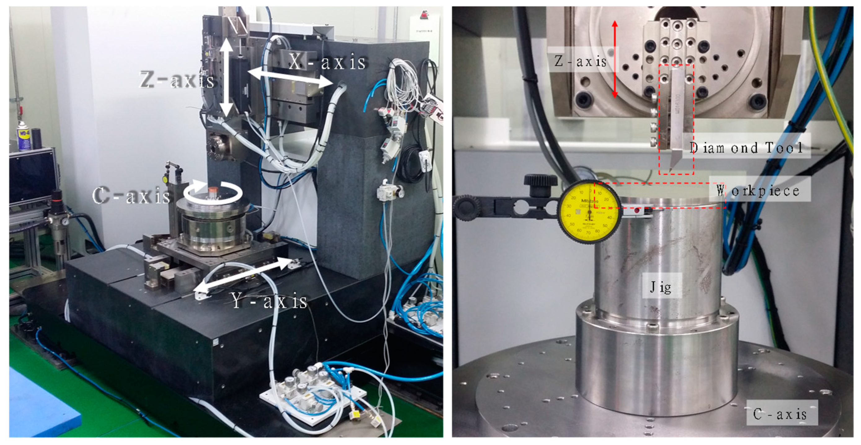
2. Experimental Setup

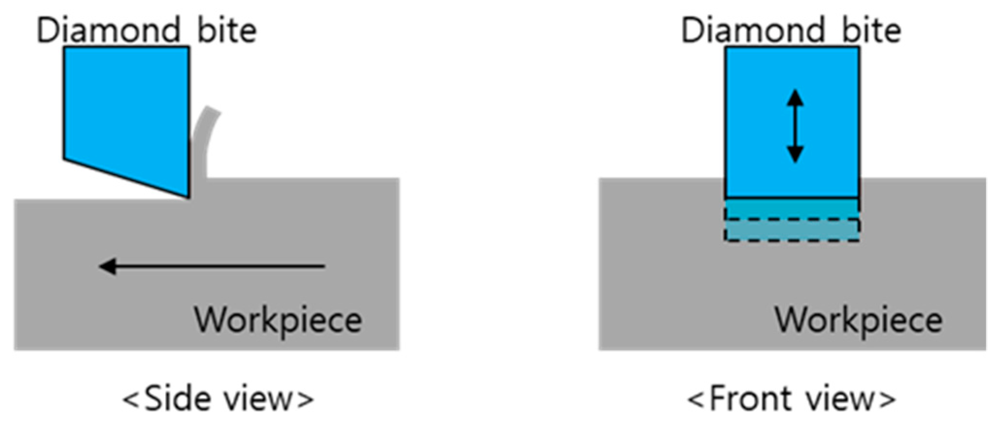
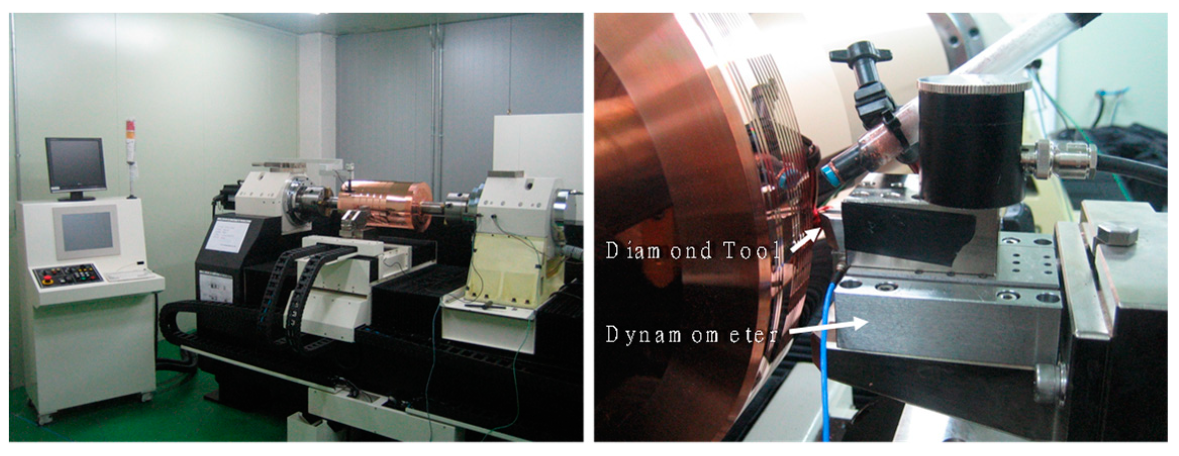
2.1. Basic Schematic of Precision Diamond Cutting

The machining experiments were carried out using precision machine tools. Microchannels of several microns in size were machined using a diamond tool. The workpiece was amorphously plated copper and nickel. Figure 1 shows a schematic of the ultra-precision turning experiment where microchannels are produced by a relative movement between a work piece and a tool.

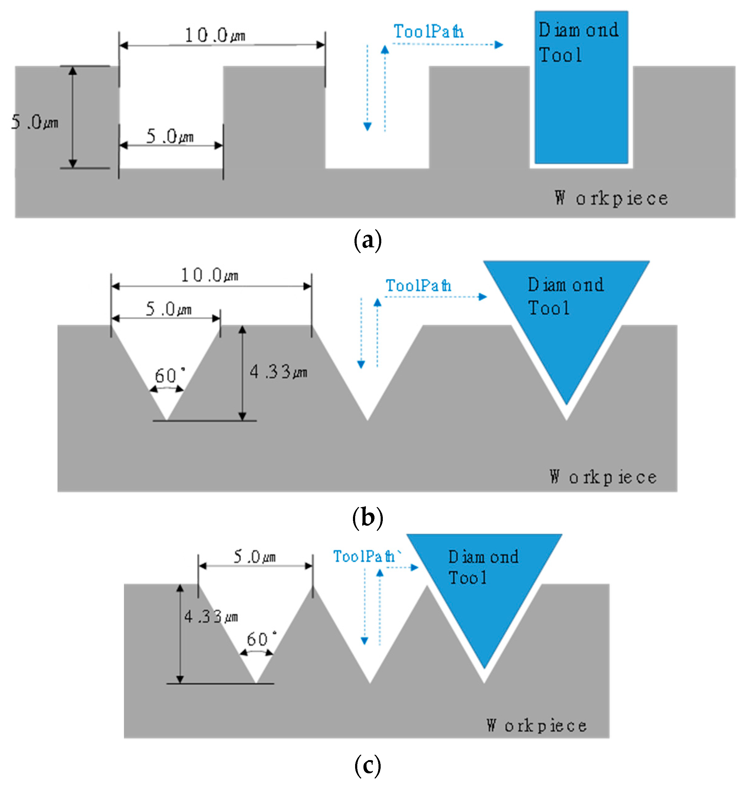
2.2. Experiments with Three Shapes of Microstructural Patterns

Figure 2 shows the experimental methods for fabricating the surface microstructures of three shapes. This experiment was devised to investigate the influence of the morphological characteristics of a surface microstructure on the shape accuracy of the microstructures. Figure 2a shows the fabrication of a microstructure where the shape of the cross-section is a quadrangle by using a rectangular tool. Figure 2b shows the fabrication of a surface microstructure with a trapezoidal cross-section using a triangular tool. Figure 2c shows the fabrication of a surface microstructure with a triangular cross-section using a triangular tool. These experiments were performed under the feed rates of 1.0 µm/rev and 0.1 µm/rev on a nickel-plated circular plate with a diameter of 90 mm. The angular velocity of a work piece was 100 rpm. Figure 3 shows the precision machine tool and experimental setup.

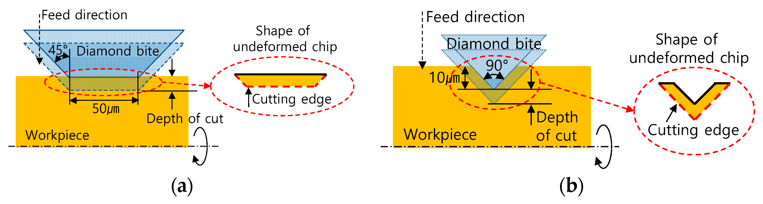
2.3. Experiments for Cutting Force Measurement

Figure 4 is a schematic drawing of the experiment to measure the cutting forces for the different cross-sectional shapes. Two shapes of tools—one with the rake face of a trapezoidal shape and the other with a triangular-shaped rake face—were examined for the two shapes (trapezoidal and V-shaped) of the cross-section. The inside of the red dotted circles in Figure 4 indicates the shape of each cross-section to be cut. In that cutting section, the red dotted line is the cutting edge that is to be contacted with a tool. These experiments were carried out on copper-plated rolls with a diameter of 300 mm. The angular velocity of a roll was 300 rpm, and the cutting depth was in 1-µm increments from 1 µm to 20 µm. Figure 5 shows the precision machine tool and experimental setup.

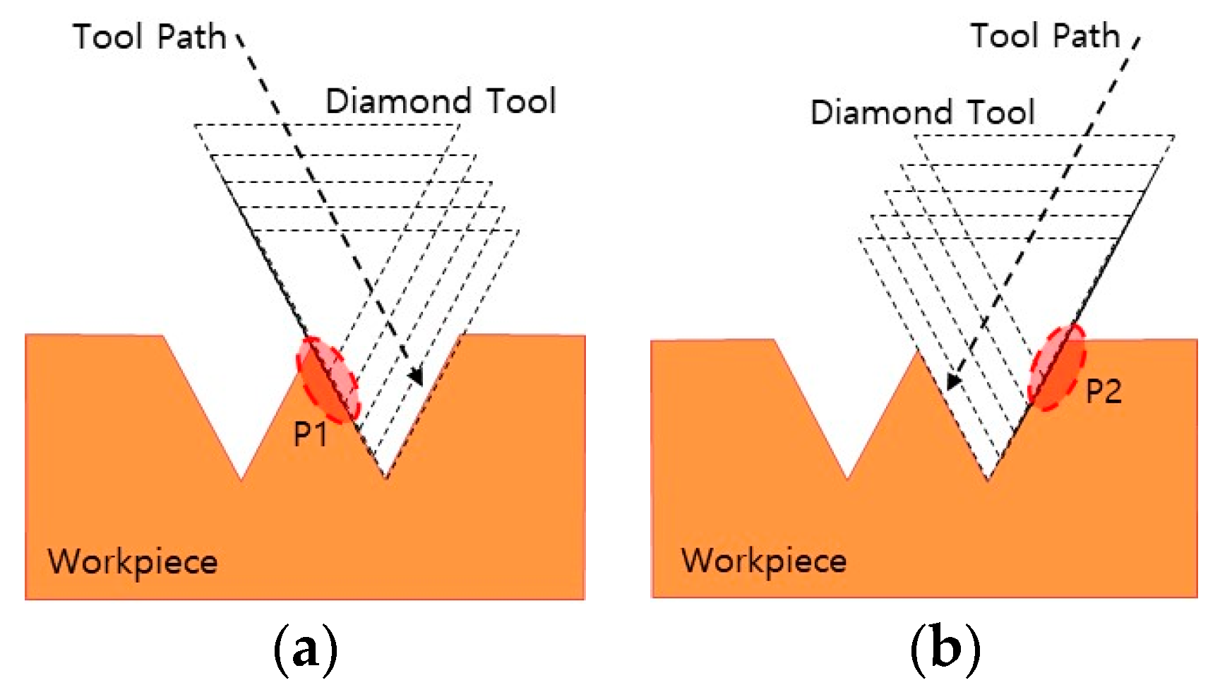
2.4. Experiments with Different Tool Paths

In order to examine the effects of a tool path on the deformation behavior of a surface microstructure, two tool paths, as shown in Figure 6, which were both different from the original one shown in Figure 2c, were devised to machine microstructural patterns with a triangular cross-section. These new tool paths (introduced in Figure 6a,b) were in a direction parallel to the slopes of a triangular microstructure, but the cutting edges—as well as the machining directions between these two paths—were different, although the final microstructural patterns were the same. These experiments were carried out on a copper-plated circular plate with a diameter of 50 mm. The speed of a work piece was 4 m/min, and the depth of each cut was 1 µm. The precision machine tool used in these experiments was the same as those described in Section 2.2.

3. Results and Discussion

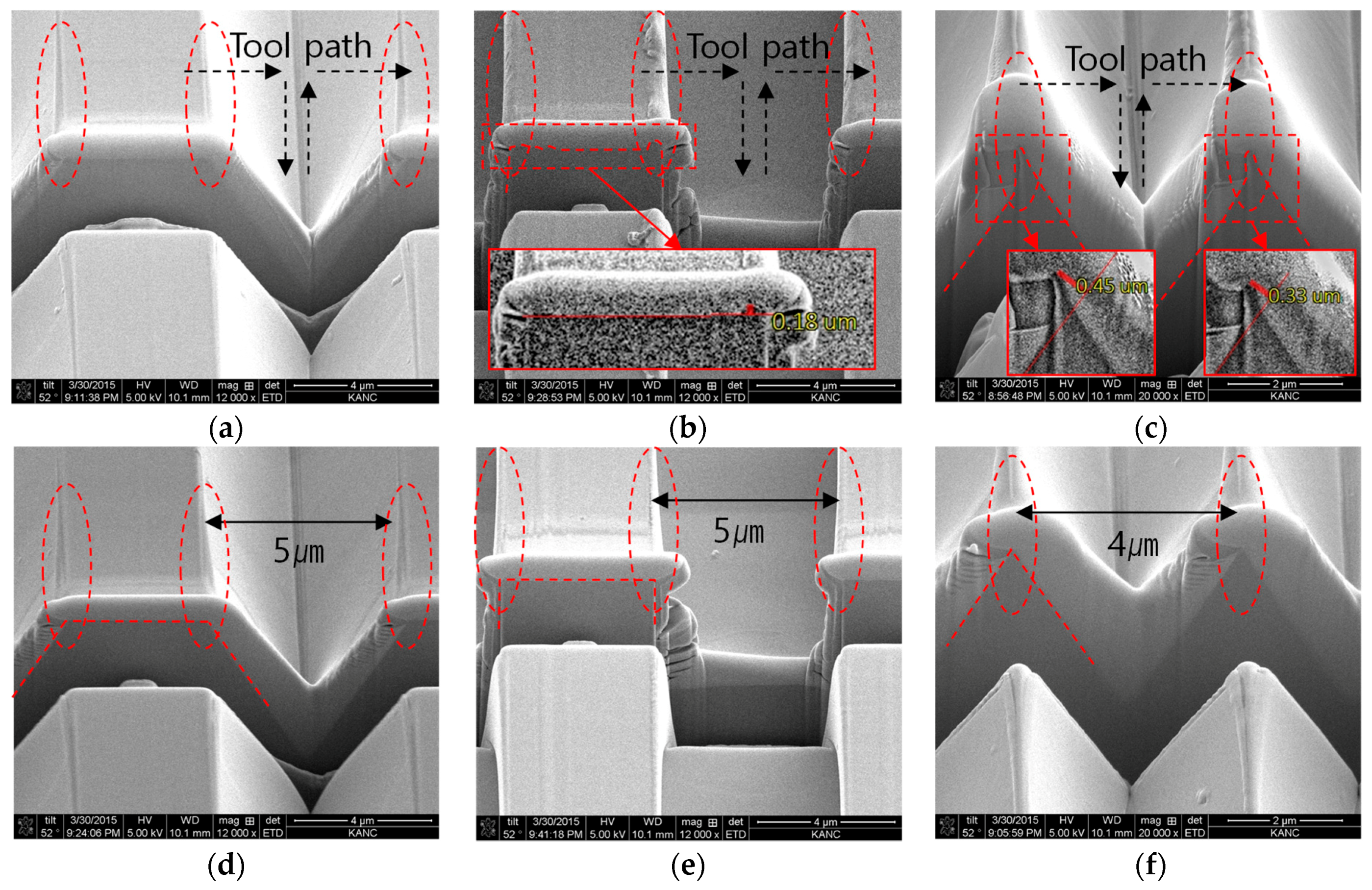
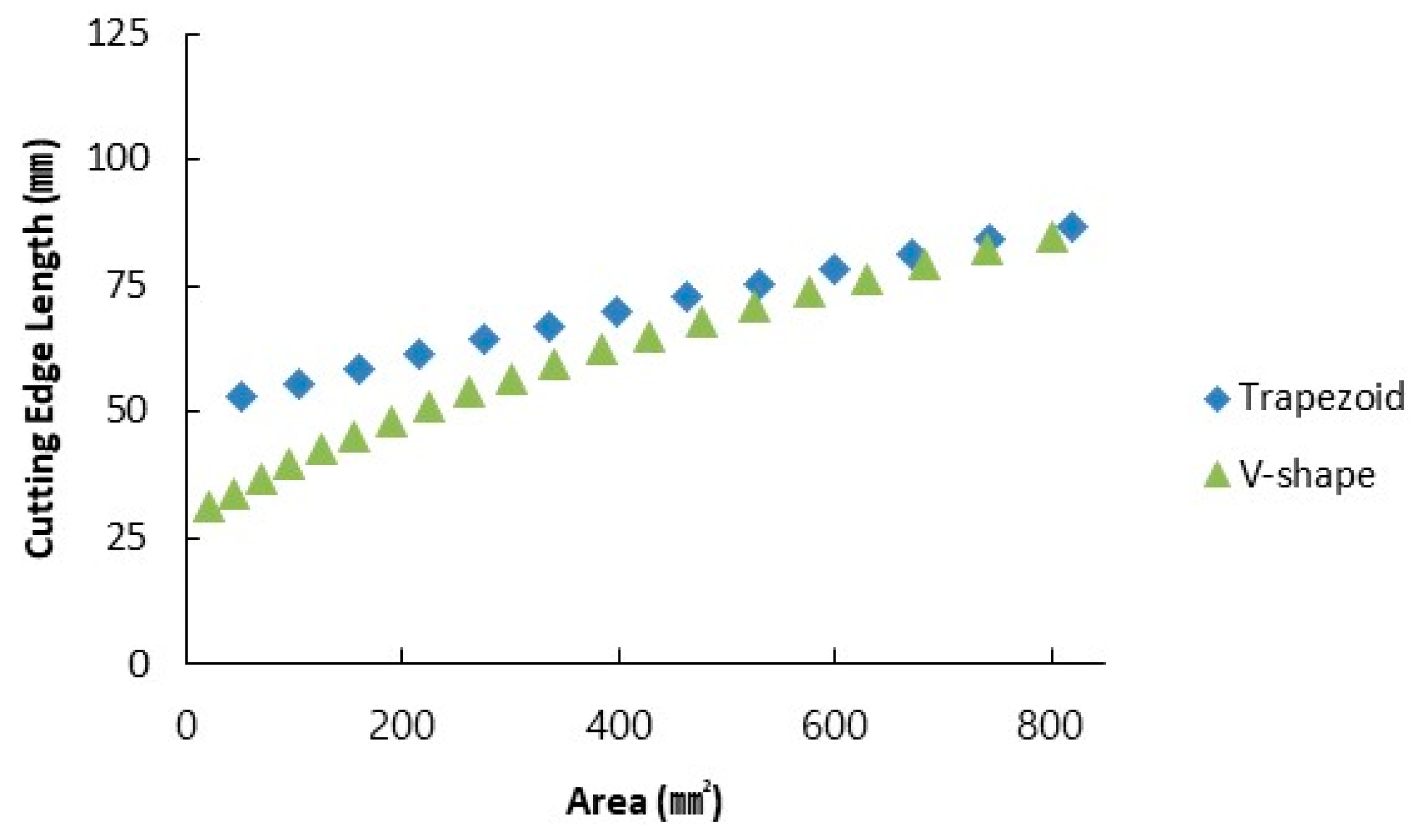
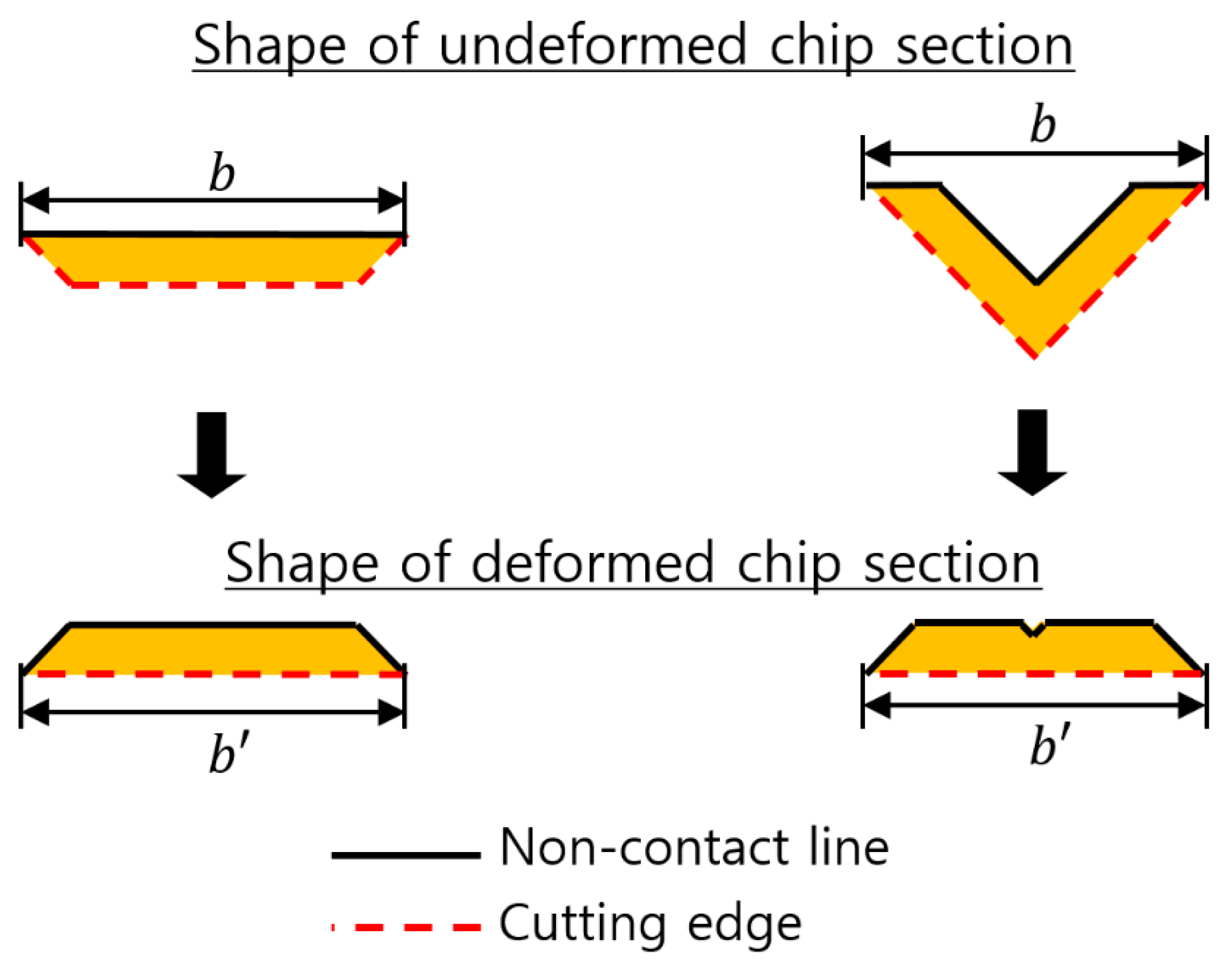
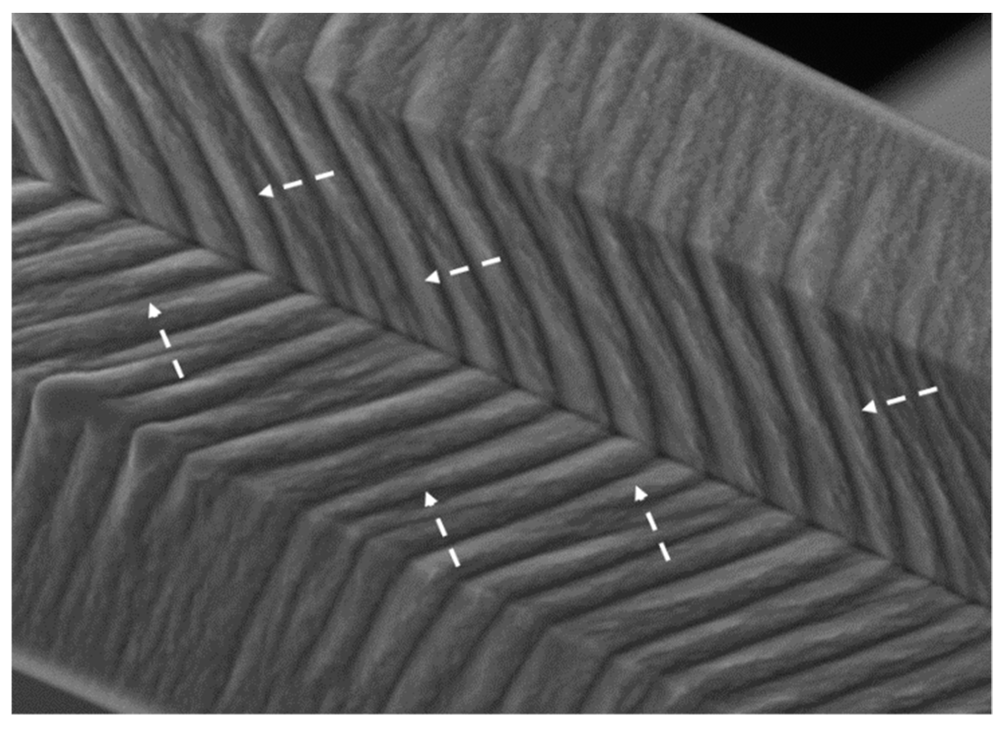
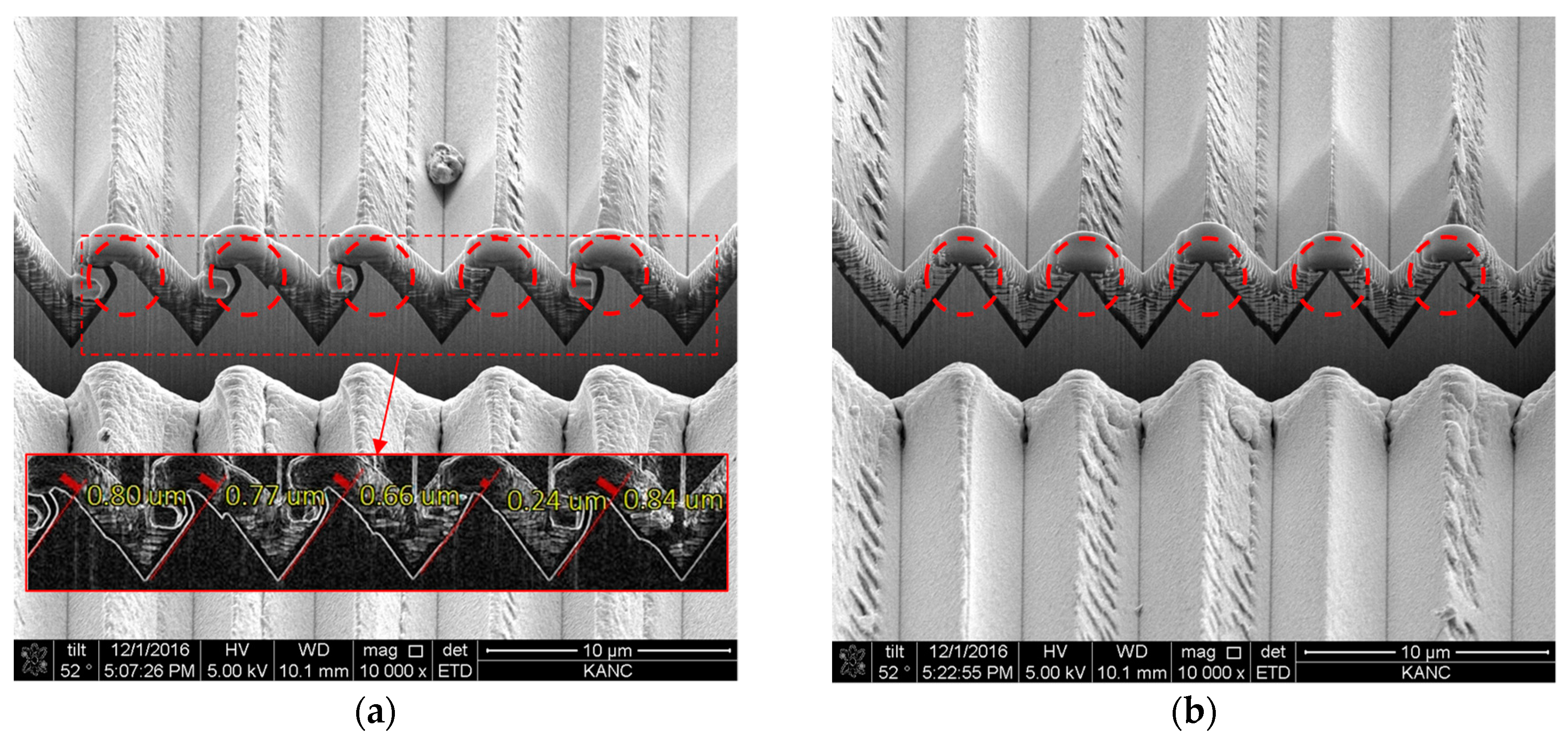
3.1. Effects of the Shape of the Microstructure
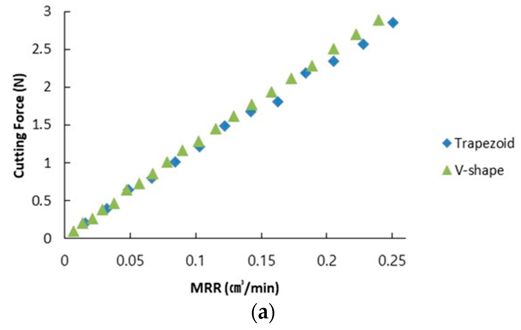
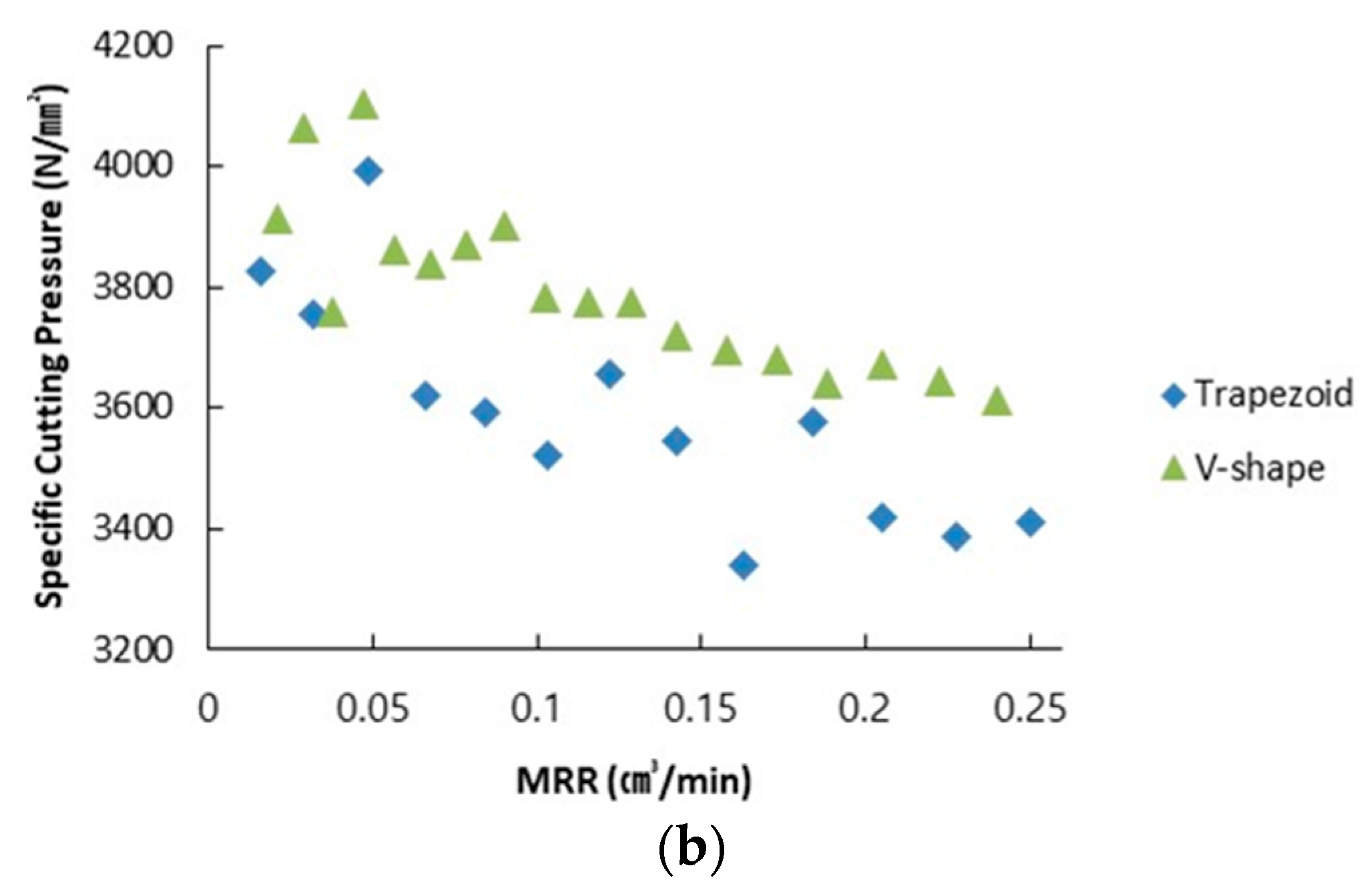
Figure 7 presents the images obtained by observing the three shapes of the machined microstructures by SEM. In order to observe each machined result more clearly, the cross-section of the microstructures was formed by the FIB (focused ion beam) milling process, and then observed with SEM. In order to minimize the shape changes of a cross-section during the FIB milling process, Pt (platinum) was deposited on the microstructure before the FIB milling process commenced.
The microstructures with a trapezoidal cross-sectional shape did not show any burrs or deformation when the depth of cut was 1 µm or 0.1 µm. As a result of the square-shaped microstructures, burrs of about 0.18 µm that formed at the upper edge were observed under the machining conditions of a 1-µm depth of cut. Burrs were not observed under the condition where the depth of cut was reduced to 0.1 µm. In microstructures with a triangular cross-section, a deformation of about 0.39 µm occurred under a machining condition with a depth of cut of 1 µm. This shape error did not occur under the machining conditions with a depth of cut of 0.1 µm.
To et al. reported that deformation of the microstructure of the material surface increased when the depth of cut was increased in precision machining. Studies by Yan et al. and Kim et al. showed that the shape accuracy improved when the depth of cut was reduced [9,10,11]. In this experiment, the relationship between the depth of cut and shape error was similar to the results obtained by other researchers.
The experiments showed that the different results depended on the shape of the microstructure in the experiments when using similar machining conditions. For the case of a cutting depth of 1 µm, the shape error types according to the shape of the microstructure are obtained from Figure 6 by using the diagrams. Burrs or deformation did not occur in the case where the angle between the surface contacting the tool and the adjacent surface was 120° (a microstructure with a trapezoidal cross-section). In the case of 90° (a microstructure with a rectangular cross-section), a burr formed at the upper edge of the microstructure. When the angle was 60° (microstructure where the shape of the cross-section is triangular), local deformation occurred at the upper edge of the microstructure. The experimental results showed that the shape error tended to be larger when the angle between the surface in contact with the tool and the adjacent surface at the time of machining the microstructure was smaller. These shape errors did not appear when the depth of cut had been reduced to 0.1 µm.
The shape errors of the microstructures of several microns in size occurred intensively at the upper edge of the microstructure. It was found that the form accuracy of the microstructure changed depending on the angle between the surface that comes into contact with the tool and the adjacent surface in the experimental results of the fabrication of the three kinds of microstructures. Figure 8 summarizes these phenomena. It should also be noted that if the form accuracy of the microstructure is improved due to the reduction of the depth of cut, the productivity will decrease because the machining time is increased.

3.2. Cutting Force

Cutting forces were measured while machining the two cross-sectional shapes, as described in Section 2.3. Then, the specific cutting pressure was calculated from the measured cutting forces.
Figure 9a shows the cutting force measured during the experiment in Section 2.3 versus the MRR (material removal rate), and Figure 9b shows the specific cutting pressure calculated based on the cutting force versus the MRR. The experimental results showed that the cutting force of the V-shaped cutting cross-section was slightly larger than that of the trapezoidal cutting cross-section, even though the material removal rate was the same. Additionally, the specific cutting pressure calculated based on the cutting force was slightly larger.
Since the machining speeds of the two cases were the same, it is conceivable that the machining cross-sectional area is the same if the material removal rates are the same. Figure 10 shows the length of the cutting edge according to the change in the cross-sectional area for the two cross-sectional shapes. When the cross-sectional area of the cutting was the same, the length of the cutting edge for the V-shaped cross-section was shorter than that for the trapezoidal one. Thus, the chip thickness of the trapezoidal cross-section was smaller than that of the V-shaped cross-section in this study. In general, the cutting force is expected to be larger when the chip thickness is smaller [23,24,25,26,27]. This is very true if the cross-sectional shapes to be cut are very similar or the same. The experiment results in this study were not consistent with those in previous works due to a slight difference between the shapes of the trapezoidal and triangular cross-sections. The difference in the cutting forces in this study might be expressed by considering the formation and deformation of a chip in two machining processes.
Figure 11 shows a SEM image of the shape of the machined chip. Figure 12 shows the changes in the cross-sectional shape of the chip before and after machining the two cross-sectional shapes based on the SEM image in Figure 11. Figure 12 b represents the width of the cross-section of cutting, and Figure 12 b′ represents the width of the cross-section of the chip generated after machining.
Table 1 and Table 2 show the change in the width of the cross-section before and after machining for the two cross-sectional shapes. Figure 12 b is a value calculated from a machining condition and a tool shape, and Figure 12 b′ is a value measured from an SEM image of the chip. In the case of the trapezoidal cross-sectional shape, the width of the chip generated after machining was larger. In the case of the V-shaped cross-section, the width of the cross-section of the chip generated after machining was smaller than the width of the cross-section before machining when the depth of cut was 5 µm. When the depth of cut was 10 µm, the width of the chip generated after machining was larger, but the difference was smaller than that in case of the trapezoidal cross-sectional shape.
Figure 13 shows an enlarged view of part of the SEM image shown in Figure 11b. A close look at the V-shaped combs generated by the triangular-shaped tool shows that the wrinkled areas in the oblique direction to the V-shaped combs appeared intermittently (as indicated by the dotted arrow). From the results, it can be seen that there was a chip flow in the center around the vertex of the triangular-shaped tool in the shear deformation process to generate the chip. The flow of this type of chip has also been mentioned by Yan et al. [10].
To summarize the cutting force experiments, the plastic deformations of the chips for the two machining processes were different, even if the cross-sectional areas to be cut for the two processes were the same. A V-shaped cross-section resulted in a more complex shape change in the chip formation than the trapezoidal cross-section. Correspondingly, the required cutting load for the V-shaped cross-section was higher than the trapezoidal cross-section. It can be concluded that the cross-sectional shape is an important factor affecting the cutting load. Thus, engineers should design the shape of the cutting cross-section in order to reduce the cutting load when planning a tool path.

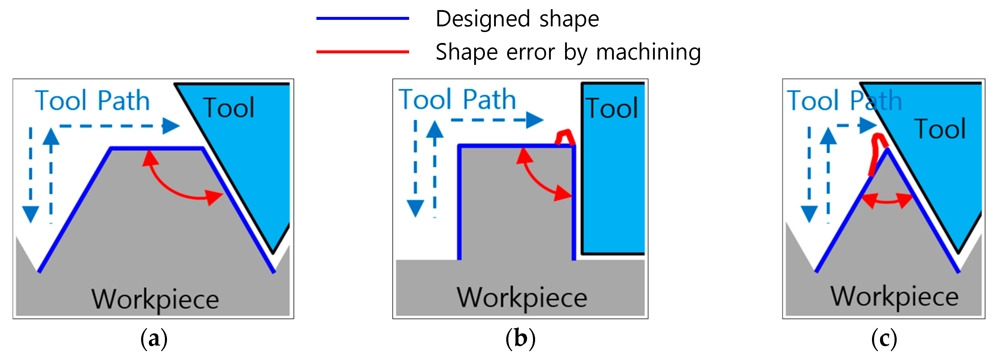
3.3. Tool Path Change

From the results detailed in Section 3.1, if the part stressed by the continuous contact of the diamond tool during machining (as shown in Figure 6a) is a weakly shaped area (‘P1’ position), it causes a large shape error, as shown in Figure 14a. Figure 14a, which shows the result of machining using the toolpath of Figure 6a, clearly demonstrates the results discussed in Section 3.1.
Therefore, an improved tool path was devised, as shown in Figure 6b, so that the area with high stress during machining had a shape with high rigidity (‘P2’ position). This also took into account the advantages of the cutting cross-section of a simple shape, as discussed in Section 3.2.
Figure 14b shows the machining results for this improved tool path while maintaining a DOC of 1 µm. The micropatterns were created accurately, and the improved toolpath enhanced the shape accuracy of the micropattern without reducing the production efficiency.

4. Conclusions

The main objective of this study was to reduce the shape error without decreasing the production efficiency in the precision machining of microstructures with a triangular cross-section with a width of 5 µm or less.
First, the characteristics of the shape errors according to the geometric shapes of the microstructures were examined. Microstructures with three cross-sectional shapes (rectangular, trapezoidal, and triangular) were fabricated to observe the occurrence of the shape errors. When the DOC was 1 μm, the trapezoidal microstructure with an angle of 120° between the cutting surface and the adjacent surface had no shape error. A burr of about 0.18 µm was formed in the rectangular microstructures with an angle of 90° between the cutting surface and the adjacent surfaces. Additionally, deformation of about 0.39 µm occurred in the triangular microstructures of 60°. In the case of a DOC of 0.1 µm, no shape error occurred in all three cases. Second, the cutting loads on two cutting cross-sectional shapes, such as the trapezoidal and V-shaped cross-section, were compared. The cutting load was smaller when the shape of the cutting cross-section was a relatively simple trapezoidal shape.
Based on these experimental results, the tool path was modified. The paths were arranged diagonally so that the tools proceeded side by side on the shape surface of the triangular microstructure. Due to the tool path change, the shape of the cutting cross-section changed from a V-shape to the simpler trapezoidal shape. Furthermore, the angle between the cutting surface and the adjacent surface increased from 60° to 120°. Before the tool path was modified, the deformation of the triangular micropattern under the condition of a DOC of 1 µm was about 0.39 µm, but no deformation occurred after the tool path was modified. As a result, the shape accuracy of the triangular microstructures was improved without reducing the production efficiency.

Author Contributions

K.-H.S. carried out the experiments, analyzed the data, and wrote the paper; Y.-J.C. led the research; and Y.-S.L. supervised all parts in this paper.

Funding

This research was funded by the Ministry of Trade, Industry, and Energy of the Republic of Korea, grant number 20000285.

Acknowledgments

The authors are thankful to Kang Kim at Kookmin University for his valuable comments and advice. K.S. and Y.C. wish to acknowledge the Ministry of Trade, Industry, and Energy of the Republic of Korea for supporting this work under grant numbers 20000285 and 10042584.

Conflicts of Interest

The authors declare no conflicts of interest.

References

  1. Wang, Z.; Zhang, H.; Fu, R.; Mu, G.; Lu, Z.; Cartwright, C.M.; Gillespie, W.A. Hybrid Diffractive-Refractive Ultra-Wide-Angle Eyepieces. Optik 2002, 113, 159–162. [Google Scholar] [CrossRef]
  2. Becker, H.; Gärtner, C. Polymer Microfabrication Technologies for Microfluidic Systems. Anal. Bioanal. Chem. 2008, 390, 89–111. [Google Scholar] [CrossRef] [PubMed]
  3. Jang, H.S.; Park, D.S. Microfabrication of Microchannels for Fuel Cell Plates. Sensors 2010, 10, 167–175. [Google Scholar] [CrossRef]
  4. Sun, J.; Luo, X.; Chang, W.; Ritchie, J.M.; Chien, J.; Lee, A. Fabrication of Periodic Nanostructures by Single-Point Diamond Turning with Focused Ion Beam Built Tool Tips. J. Micromech. Microeng. 2012, 22, 115014. [Google Scholar] [CrossRef]
  5. Thiele, S.; Seifert, A.; Herkommer, A.M. Wave-Optical Design of a Combined Refractive-Diffractive Varifocal Lens. Opt. Express 2014, 22, 13347–13350. [Google Scholar] [CrossRef] [PubMed]
  6. Tien, N.X.; Shin, S. A Novel Concentrator Photovoltaic (CPV) System with the Improvement of Irradiance Uniformity and the Capturing of Diffuse Solar Radiation. Appl. Sci. 2016, 6, 251. [Google Scholar] [CrossRef]
  7. Tanaka, Y.; Yamagata, M.; Sasano, T. Diffractive-Refractive Achromatic Lens for Optical Disk System by Molding. Opt. Rev. 1998, 5, 334–339. [Google Scholar] [CrossRef]
  8. Masuzawa, T. State of the Art of Micromachining. Ann. CIRP 2000, 49, 473–488. [Google Scholar] [CrossRef]
  9. To, S.; Zhu, Y.H.; Lee, W.B. Effect of Cutting Depth on the Surface microstructure of a Zn-Al Alloy during Ultra-Precision Machining. Appl. Surf. Sci. 2008, 254, 1559–1564. [Google Scholar] [CrossRef]
  10. Yan, J.; Oowada, T.; Zhou, T.; Kuriyagawa, T. Precision Machining of Microstructures on Electroless-Plated Nip Surface for Molding Glass Components. J. Mater. Process. Technol. 2009, 209, 4802–4808. [Google Scholar] [CrossRef]
  11. Kim, G.D.; Loh, B.G. Machining of Micro-Channels and Pyramid Patterns Using Elliptical Vibration Cutting. Int. J. Adv. Manuf. Technol. 2010, 49, 961–968. [Google Scholar] [CrossRef]
  12. Zhang, X.; Gao, H.; Guo, Y.; Zhang, G. Machining of optical freeform prisms by rotating tools turning. CIRP Ann. Manuf. Technol. 2012, 61, 519–522. [Google Scholar] [CrossRef]
  13. Duong, T.H.; Kim, H.C.; Lee, D.Y.; Lee, S.W.; Park, E.S.; Je, T.J. A Theoretical Deformation Prediction of Micro Channels in Ultra-Precision Machining. Int. J. Precis. Eng. Manuf. 2013, 14, 173–181. [Google Scholar] [CrossRef]
  14. Duong, T.H.; Kim, H.C. Deformation Analysis of Rectangular Channel Structures in Micro Pattern machining. Int. J. Precis. Eng. Manuf. 2015, 16, 619–627. [Google Scholar] [CrossRef]
  15. Tauhiduzzaman, M.; Yip, A.; Veldhuis, S.C. Form Error in Diamond Turning. Precis. Eng. 2015, 42, 22–36. [Google Scholar] [CrossRef]
  16. Lee, K.; Dornfeld, D.A. Micro-Burr Formation and Minimization through Process Control. Precis. Eng. 2005, 29, 246–252. [Google Scholar] [CrossRef]
  17. Zhang, J.; Cui, T.; Ge, C.; Sui, Y.; Yang, H. Review of Micro/Nano Machining by Utilizing Elliptical Vibration Cutting. Int. J. Mach. Tools Manuf. 2016, 106, 109–126. [Google Scholar] [CrossRef]
  18. Siitonen, S.; Pietarinen, J.; Laakkonen, P.; Jefimovs, K.; Kuittinen, M.; Alajoki, T.; Mönkkönen, K.; Pääkkönen, E.J.; Tervonen, A. Replicated Polymer Light Guide Interconnector with Depth Modified Surface Relief Grating Couplers. Opt. Rev. 2007, 14, 304–309. [Google Scholar] [CrossRef]
  19. Attia, U.M.; Marson, S.; Alcock, J.R. Micro-Injection Moulding of Polymer Microfluidic Devices. Microfluid. Nanofluid. 2009, 7, 1. [Google Scholar] [CrossRef]
  20. Kobayashi, R.; Xu, S.; Shimada, K.; Mizutani, M.; Kuriyagawa, T. Defining the Effects of Cutting Parameters on Burr Formation and Minimization in Ultra-Precision Grooving of Amorphous Alloy. Precis. Eng. 2017, 49, 115–121. [Google Scholar] [CrossRef]
  21. Yan, Y.; Hu, Z.; Zhao, X.; Sun, T.; Dong, S.; Li, X. Top-Down Nanomechanical Machining of Three-Dimensional Nanostructures by Atomic Force Microscopy. Small 2010, 6, 724–728. [Google Scholar] [CrossRef] [PubMed]
  22. Yan, Y.; Geng, Y.; Hu, Z. Recent Advances in AFM Tip-Based Nanomechanical Machining. Int. J. Mach. Tools Manuf. 2015, 99, 1–18. [Google Scholar] [CrossRef]
  23. Furukawa, Y.; Moronuki, N. Effect of Material Properties on Ultra Precise Cutting Processes. Ann. CIRP 1988, 37, 113–116. [Google Scholar] [CrossRef]
  24. Ng, C.K.; Melkote, S.N.; Rahman, M.; Kumar, A.S. Experimental Study of Micro- and Nano-scale Cutting of Aluminum 7075-T6. Int. J. Mach. Tools Manuf. 2006, 46, 929–936. [Google Scholar] [CrossRef]
  25. Weber, M.; Autenrieth, H.; Kotschenreuther, J.; Gumbsch, P.; Schulze, V.; Löhe, D.; Fleisher, J. Influence of Friction and Process Parameters on the Specific Cutting Force and Surface Characteristics in Micro Cutting. Mach. Sci. Technol. 2008, 12, 474–497. [Google Scholar] [CrossRef]
  26. Zhang, T.; Liu, Z.; Shi, Z.; Xu, C. Size Effect on Surface Roughness in Micro Turning. Int. J. Precis. Eng. Manuf. 2013, 14, 345–349. [Google Scholar] [CrossRef]
  27. Oliveira, F.B.; Rodrigues, A.R.; Coelho, R.T.; Souza, A.F. Size Effect and Minimum Chip Thickness in Micromilling. Int. J. Mach. Tools Manuf. 2015, 89, 39–54. [Google Scholar] [CrossRef]
Figure 1. Schematic drawing of an ultra-precision machining experiment. The left shows the generation of chip by relative transport of tool and material. The right shows the process of dividing the whole cutting depth and cutting it sequentially.
Applsci 09 02940 g001
Figure 2. Three shapes of microstructural patterns: (a) with rectangular cross-sections; (b) trapezoidal cross-sections; (c) triangular cross-sections.
Applsci 09 02940 g002
Figure 3. Precision machine tool (4-axis with air bearing) and experimental setup setup(run-out correction using the indicator and height correction using a jig).
Applsci 09 02940 g003
Figure 4. Cutting force measurement for the different section shapes: (a) trapezoidal section shape, (b) V-shaped sectional shape.
Applsci 09 02940 g004
Figure 5. Precision drum lathe and experimental setting. A tool dynamometer was used to measure the cutting force.
Applsci 09 02940 g005
Figure 6. Machining with different tool paths: (a) changed tool path 1 (continuous contact area ‘P1’), (b) changed tool path 2 (continuous contact area ‘P2’).
Applsci 09 02940 g006
Figure 7. SEM photos for the three shapes of the machined microstructures: depth of cut of 1.0 µm (ac) and 0.1 µm (df).
Applsci 09 02940 g007
Figure 8. Illustration of the shape error of three microstructural patterns: (a) trapezoidal cross-sections, (b) rectangular cross-sections, and (c) triangular cross-sections.
Applsci 09 02940 g008
Figure 9. Measured cutting force and specific cutting pressure: (a) cutting force, (b) specific cutting pressure.
Applsci 09 02940 g009aApplsci 09 02940 g009b
Figure 10. Cutting edge length.
Applsci 09 02940 g010
Figure 11. SEM images of the cutting chips: (a) cutting chip of the trapezoidal section, (b) cutting chip of the V-shaped section.
Applsci 09 02940 g011
Figure 12. Illustration of chip deformation. (b: undeformed chip width, b′: deformed chip width).
Applsci 09 02940 g012
Figure 13. Machined chip SEM image of the V-shaped section. The dotted arrow indicates the flow direction of the chip.
Applsci 09 02940 g013
Figure 14. Machining results on the changed tool path: (a) the machining result obtained by using the tool path shown in Figure 6a, and (b) the machining result obtained by using the tool path shown in Figure 6b.
Applsci 09 02940 g014
Table 1. Undeformed chip width and chip width of the trapezoidal section shape.
Cutting Depth (µm)b (µm)b′ (µm)
107074.9
209095.4
Table 2. Undeformed chip width and chip width of the V-shaped section shape.
Cutting Depth (µm)b (µm)b′ (µm)
53028.5
104041.2

