Impact of Silicon Substrate with Low Resistivity on Vertical Leakage Current in AlGaN/GaN HEMTs


 ,
, 
Abstract
1. Introduction
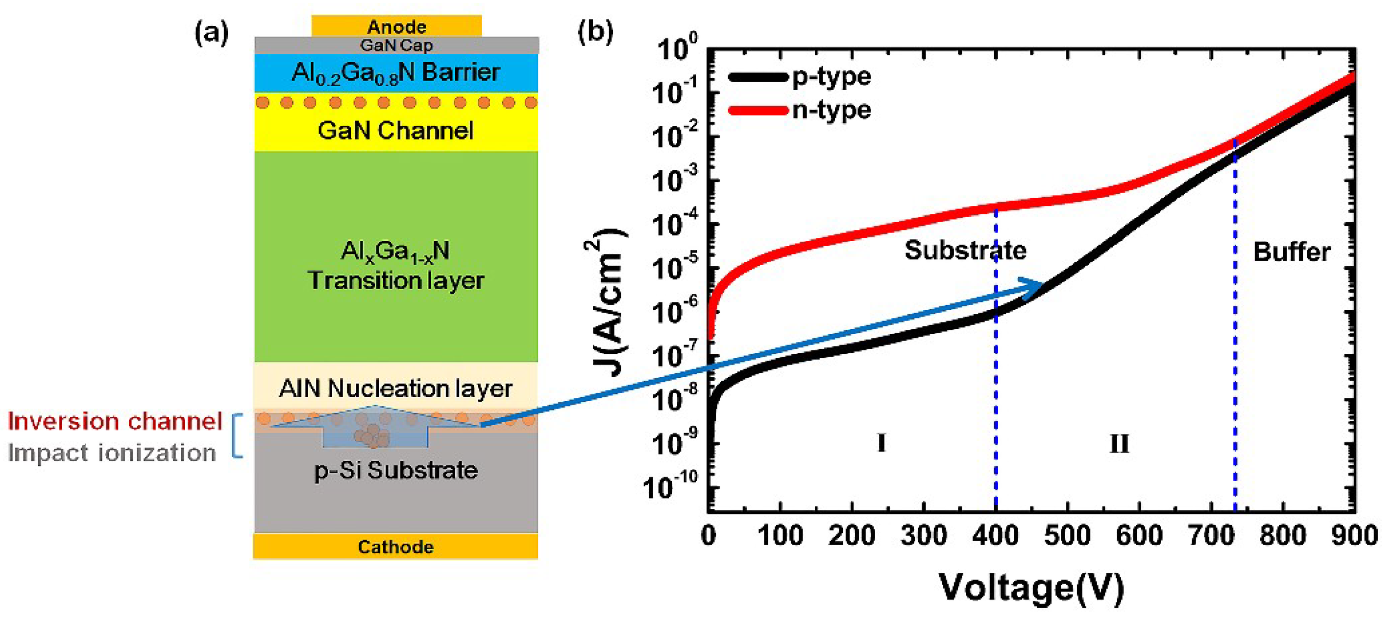
2. Experiments
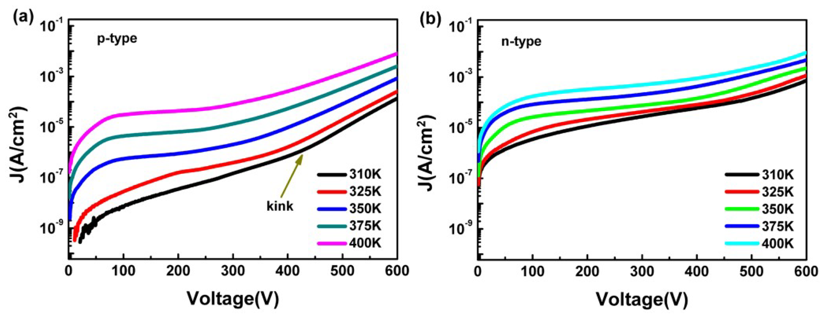
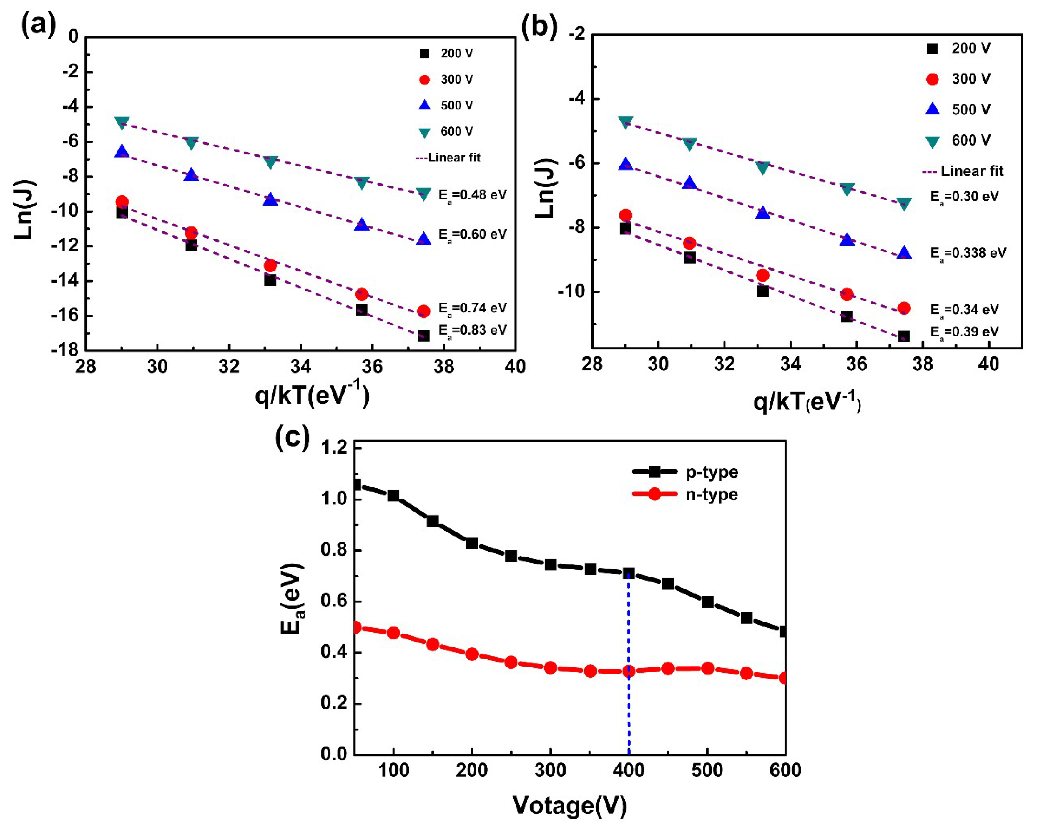
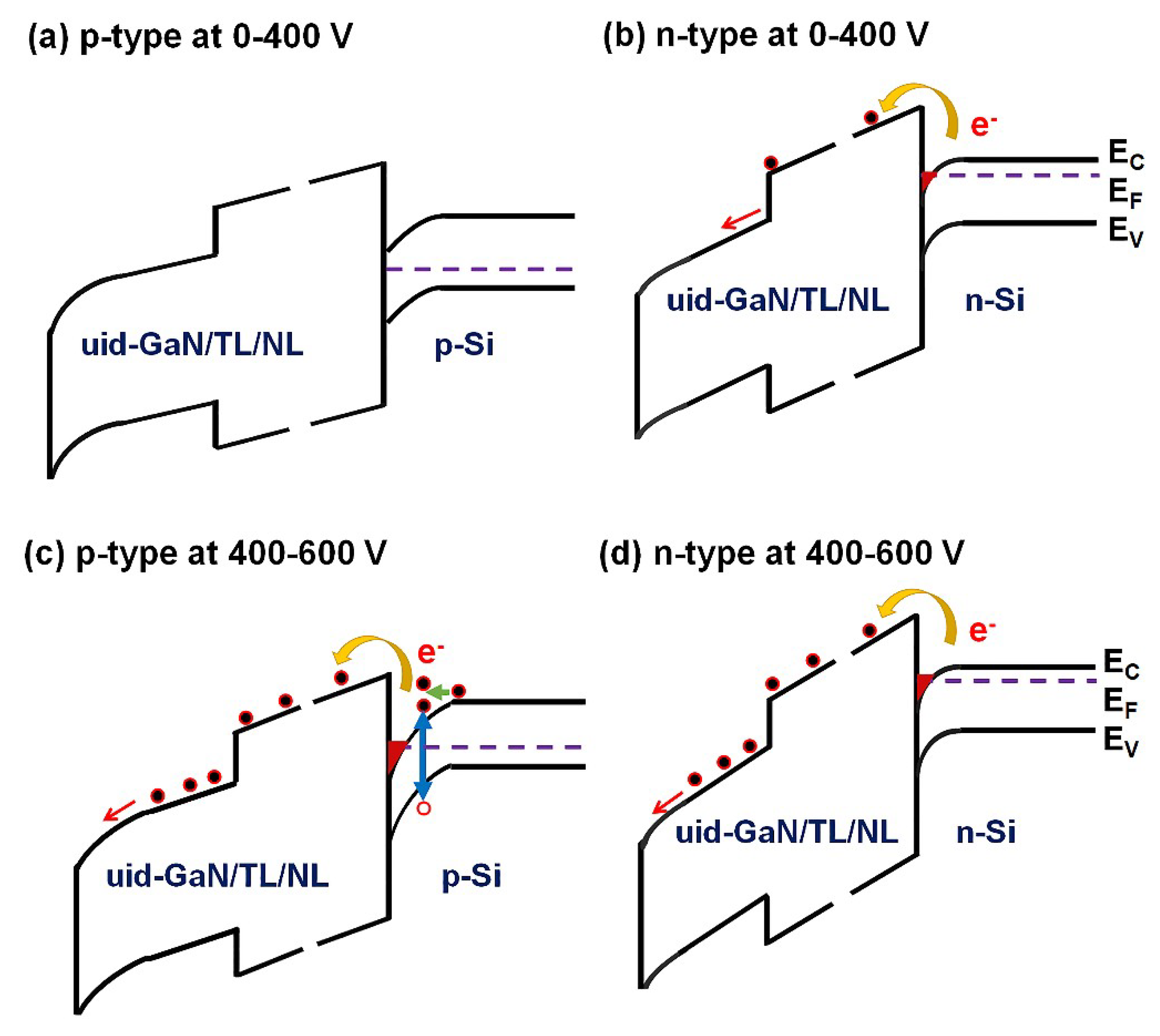
3. Results and Discussion
4. Conclusions
Author Contributions
Funding
Conflicts of Interest
References
- Liu, M.; Zhao, J.; Zhou, S.; Gao, Y.; Hu, J.; Liu, X.; Ding, X. An InGaN/GaN Superlattice to Enhance the Performance of Green LEDs: Exploring the Role of V-Pits. Nanomaterials 2018, 8, 450. [Google Scholar] [CrossRef] [PubMed]
- Sun, Y.; Zhou, K.; Feng, M.; Li, Z.; Zhou, Y.; Sun, Q.; Liu, J.; Zhang, L.; Li, D.; Sun, X.; et al. Room-temperature continuous-wave electrically pumped InGaN/GaN quantum well blue laser diode directly grown on Si. Light. Sci. Appl. 2018, 7, 13. [Google Scholar] [CrossRef] [PubMed]
- Ahmadivand, A.; Sinha, R.; Vabbina, P.K.; Karabiyik, M.; Kaya, S.; Pala, N. Hot electron generation by aluminum oligomers in plasmonic ultraviolet photodetectors. Opt. Express 2016, 24, 13665. [Google Scholar] [CrossRef] [PubMed]
- Li, D.; Sun, X.; Song, H.; Li, Z.; Chen, Y.; Jiang, H.; Miao, G. Realization of a High-Performance GaN UV Detector by Nanoplasmonic Enhancement. Adv. Mater. 2012, 24, 845–849. [Google Scholar] [CrossRef]
- Kwak, H.-T.; Chang, S.-B.; Kim, H.-J.; Jang, K.-W.; Yoon, H.S.; Lee, S.-H.; Lim, J.-W.; Kim, H.-S. Operational Improvement of AlGaN/GaN High Electron Mobility Transistor by an Inner Field-Plate Structure. Appl. Sci. 2018, 8, 974. [Google Scholar] [CrossRef]
- Chiu, H.-C.; Peng, L.-Y.; Yang, C.-W.; Wang, H.-C.; Mai, K.-D.; Kao, H.-L.; Tung, C.-K.; Chang, T.-C.; Hon, S.-J.; Lin, J.-C.; et al. Normally-off matrix layout p-GaN gate AlGaN/GaN power HEMT with a through-substrate via process. J. Vac. Sci. Technol. B 2016, 34, 21205. [Google Scholar] [CrossRef]
- Borga, M.; Meneghini, M.; Stoffels, S.; Li, X.; Posthuma, N.; Van Hove, M.; Decoutere, S.; Meneghesso, G.; Zanoni, E. Impact of Substrate Resistivity on the Vertical Leakage, Breakdown, and Trapping in GaN-on-Si E-Mode HEMTs. IEEE Trans. Electron Devices 2018, 65, 2765–2770. [Google Scholar] [CrossRef]
- Hu, A.; Yang, X.; Cheng, J.; Song, C.; Zhang, J.; Feng, Y.; Ji, P.; Xu, F.; Zhang, Y.; Yang, Z.; et al. Vertical leakage induced current degradation and relevant traps with large lattice relaxation in AlGaN/GaN heterostructures on Si. Appl. Phys. Lett. 2018, 112, 032104. [Google Scholar] [CrossRef]
- Umeda, H.; Suzuki, A.; Anda, Y.; Ishida, M.; Ueda, T.; Tanaka, T.; Ueda, D. Blocking-voltage boosting technology for GaN transistors by widening depletion layer in Si substrates. In Proceedings of the 2010 International Electron Devices Meeting, San Francisco, CA, USA, 6–8 December 2010; p. 480. [Google Scholar]
- Yang, S.; Zhou, C.; Han, S.; Wei, J.; Sheng, K.; Chen, K.J. Impact of Substrate Bias Polarity on Buffer-Related Current Collapse in AlGaN/GaN-on-Si Power Devices. IEEE Trans. Electron Devices 2017, 64, 5048–5056. [Google Scholar] [CrossRef]
- Sayadi, L.; Häberlen, O.; Fiori, G.; Knuuttila, L.O.; Curatola, G. The Role of Silicon Substrate on the Leakage Current Through GaN-on-Si Epitaxial Layers. IEEE Trans. Electron Devices 2017, 65, 51. [Google Scholar] [CrossRef]
- Li, X.; Van Hove, M.; Zhao, M.; Bakeroot, B.; You, S.; Groeseneken, G.; Decoutere, S. Investigation on Carrier Transport Through AlN Nucleation Layer From Differently Doped Si(111) Substrates. IEEE Trans. Electron Devices 2018, 65, 1721–1727. [Google Scholar] [CrossRef]
- Yang, Y.B.; Liu, M.G.; Chen, W.J.; Han, X.B.; Chen, J.; Lin, X.Q.; Lin, J.L.; Luo, H.; Liao, Q.; Zang, W.J.; et al. In-situ wafer bowing measurements of GaN grown on Si (111) substrate by reflectivity mapping in metal organic chemical vapor deposition system. Chin. Phys. B 2015, 24, 096103. [Google Scholar] [CrossRef]
- Jiang, Q.; Zhou, C.; Huang, S.; Chen, K.J. Vertical Leakage/Breakdown Mechanisms in AlGaN/GaN-on-Si Devices. IEEE Electron Device Lett. 2012, 33, 1132–1134. [Google Scholar]
- Cornigli, D.; Monti, F.; Reggiani, S.; Gnani, E.; Gnudi, A.; Baccarani, G. TCAD analysis of the leakage current and breakdown versus temperature of GaN-on-Silicon vertical structures. Solid-State Electron. 2016, 115, 173–178. [Google Scholar] [CrossRef]
- Song, C.; Yang, X.; Ji, P.; Tang, J.; Hu, A.; Feng, Y.; Lin, W.; Ge, W.; Yang, Z.; Xu, F.; et al. Role of electron injection on vertical leakage in GaN-on-Si epitaxial layers. Superlattices Microstruct. 2019, 128, 199–203. [Google Scholar] [CrossRef]
- Moens, P.; Banerjee, A.; Uren, M.; Meneghini, M.; Karboyan, S.; Chatterjee, I.; Vanmeerbeek, P.; Casar, M.; Liu, C.; Salih, A.; et al. Impact of buffer leakage on intrinsic reliability of 650V AlGaN/GaN HEMTs. In Proceedings of the 2015 IEEE International Electron Devices Meeting (IEDM), Washington, DC, USA, 7–9 December 2015; pp. 35.2.1–35.2.4. [Google Scholar]
- Cornigli, D.; Reggiani, S.; Gnani, E.; Gnudi, A.; Baccarani, G.; Moens, P.; Vanmeerbeek, P.; Banerjee, A.; Meneghesso, G. Numerical investigation of the lateral and vertical leakage currents and breakdown regimes in GaN-on-Silicon vertical structures. In Proceedings of the 2015 IEEE International Electron Devices Meeting (IEDM), Washington, DC, USA, 7–9 December 2015; p. 5. [Google Scholar]
- Yang, S.; Jiang, Q.; Li, B.; Tang, Z.; Chen, K.J. GaN-to-Si vertical conduction mechanisms in AlGaN/GaN-on-Si lateral heterojunction FET structures. Phys. Status Solidi C 2014, 11, 949–952. [Google Scholar] [CrossRef]
- Yacoub, H.; Fahle, D.; Finken, M.; Hahn, H.; Blumberg, C.; Prost, W.; Kalisch, H.; Heuken, M.; Vescan, A. The effect of the inversion channel at the AlN/Si interface on the vertical breakdown characteristics of GaN-based devices. Semicond. Sci. Technol. 2014, 29, 115012. [Google Scholar] [CrossRef]
- Remesh, N.; Mohan, N.; Kumar, S.; Prabhu, S.; Guiney, I.; Humphreys, C.J.; Raghavan, S.; Muralidharan, R.; Nath, D.N. Vertical Current Transport in AlGaN/GaN HEMTs on Silicon: Experimental Investigation and Analytical Model. IEEE Trans. Electron Devices 2019, 66, 613. [Google Scholar] [CrossRef]
- Uedono, A.; Zhao, M.; Simoen, E. Probing the effect of point defects on the leakage blocking capability of Al0.1Ga0.9N/Si structures using a monoenergetic positron beam. J. Appl. Phys. 2016, 120, 215702. [Google Scholar] [CrossRef]
- P’erez-Tom’as, A.; Fontser’e, A.; Llobet, J.; Placidi, M.; Rennesson, S.; Baron, N.; Chenot, S.; Moreno, J.C.; Cordier, Y. Analysis of the AlGaN/GaN vertical bulk current on Si, sapphire, and free-standing GaN Substrates. J. Appl. Phys. 2013, 113, 174501. [Google Scholar] [CrossRef]


| Sample Structure | Si Substrate | Vertical Leakage Mechanisms | Reference |
|---|---|---|---|
| TL/AlN/Si AlN/Si GaN-on-Si(p) | n+ p | (i) p-type: SRH carrier generation in Si (ii) n+-type: electron injection through AlN/Si barrier | [11] |
| AlN/Si | n+, p+ n, p | SCLC, VRH, and TAT models | [12] |
| GaN-on-Si | p Low resistivity | SCLC model | [14] |
| GaN-to-Si | p Low resistivity | (i) weak inversion in AlN/Si interface (ii) impact ionization in Si (iii) electron injection from Si into the Buffer | [19] |
| GaN-on-Si | p | (i) carrier injection from an inversion channel (ii) PF conduction | [20] |
| GaN-on-Si | p | PF conduction | [21] |
| (Al)GaN-on-Si | PF conduction (>200 V) | [22] | |
| GaN-on-Si | n High resistivity | a combination of PF and hopping conduction | [23] |
| (Al)GaN-on-Si | p+ n+ | (i) SCLC model at 0–400 V and PF conduction at 400–600 V for p-type (ii) SCLC model at 0–600 V for n-type (iii) impact ionization in p-Si | This work |
© 2019 by the authors. Licensee MDPI, Basel, Switzerland. This article is an open access article distributed under the terms and conditions of the Creative Commons Attribution (CC BY) license (http://creativecommons.org/licenses/by/4.0/).
Share and Cite
Song, C.; Yang, X.; Ji, P.; Tang, J.; Wu, S.; Xu, Y.; Imran, A.; Wang, M.; Yang, Z.; Xu, F.; et al. Impact of Silicon Substrate with Low Resistivity on Vertical Leakage Current in AlGaN/GaN HEMTs. Appl. Sci. 2019, 9, 2373. https://doi.org/10.3390/app9112373
Song C, Yang X, Ji P, Tang J, Wu S, Xu Y, Imran A, Wang M, Yang Z, Xu F, et al. Impact of Silicon Substrate with Low Resistivity on Vertical Leakage Current in AlGaN/GaN HEMTs. Applied Sciences. 2019; 9(11):2373. https://doi.org/10.3390/app9112373
Chicago/Turabian StyleSong, Chunyan, Xuelin Yang, Panfeng Ji, Jun Tang, Shan Wu, Yue Xu, Ali Imran, Maojun Wang, Zhijian Yang, Fujun Xu, and et al. 2019. "Impact of Silicon Substrate with Low Resistivity on Vertical Leakage Current in AlGaN/GaN HEMTs" Applied Sciences 9, no. 11: 2373. https://doi.org/10.3390/app9112373
APA StyleSong, C., Yang, X., Ji, P., Tang, J., Wu, S., Xu, Y., Imran, A., Wang, M., Yang, Z., Xu, F., Wang, X., Ge, W., & Shen, B. (2019). Impact of Silicon Substrate with Low Resistivity on Vertical Leakage Current in AlGaN/GaN HEMTs. Applied Sciences, 9(11), 2373. https://doi.org/10.3390/app9112373