Review

Progress in the Utilization Efficiency Improvement of Hot Carriers in Plasmon-Mediated Heterostructure Photocatalysis

1
Joint International Research Laboratory of Information Display and Visualization, School of Electronic Science and Engineering, Southeast University, Nanjing 210096, China
2
Key Laboratory of Micro-Inertial Instrument and Advanced Navigation Technology, Ministry of Education, School of Instrument Science and Engineering, Southeast University, Nanjing 210096, China
3
Suzhou Key Laboratory of Metal Nano-Optoelectronic Technology, Suzhou Research Institute of Southeast University, Suzhou 215123, China
*
Author to whom correspondence should be addressed.
Appl. Sci. 2019, 9(10), 2093; https://doi.org/10.3390/app9102093
Submission received: 10 April 2019 / Revised: 10 May 2019 / Accepted: 14 May 2019 / Published: 21 May 2019
(This article belongs to the Special Issue Gold Nanoparticles for Catalytic Applications)

Abstract

:
The effect of plasmon-induced hot carriers (HCs) enables the possibility of applying semiconductors with wide band gaps to visible light catalysis, which becomes an emerging research field in environmental protections. Continued efforts have been made for an efficient heterostructure photocatalytic process with controllable behaviors of HCs. Recently, it has been discovered that the improvement of the utilization of HCs by band engineering is a promising strategy for an enhanced catalytic process, and relevant works have emerged for such a purpose. In this review, we give an overview of the recent progress relating to optimized methods for designing efficient photocatalysts by considering the intrinsic essence of HCs. First, the basic mechanism of the heterostructure photocatalytic process is discussed, including the formation of the Schokkty barrier and the process of photocatalysis. Then, the latest studies for improving the utilization efficiency of HCs in two aspects, the generation and extraction of HCs, are introduced. Based on this, the applications of such heterostructure photocatalysts, such as water/air treatments and organic transformations, are briefly illustrated. Finally, we conclude by discussing the remaining bottlenecks and future directions in this field.

1. Introduction

With the demand for an eco-friendly and efficient technology for solving the bottlenecks in the fields of environments and fuels, photocatalysis has been studied in the past several decades and has been gradually applied in practice [1,2,3,4,5]. To break through the limits of photon trapping and utilization in conventional semiconductor based photocatalysts [6,7], plasmon mediated photocatalysts, via the modification of plasmonic metal on a semiconductor, is an emerging field for meeting the high requirements of developing high-performance chemical compounds [8,9], new-type fuels [10,11], and green environmental treatment techniques [12,13]. In such a heterostructure, surface plasmons (SPs) [14,15,16], a collective-electrons oscillation confined to the surface of the conductive material excited by an external electromagnetic (EM) field, is generated not only as an optical pathway, which can localize incident light from a far-field at the surface of plasmonic materials and convert photons with lower energy (visible to near-infrared regions) that the semiconductor missed. However, more impressively, SPs can also act as electrical channels for the generation and transportation of HCs (electrons and holes) after light absorption for adjacent semiconductors, for participation in further applications, such as chemical reactions.
Currently, the main mechanisms reported in such plasmon enhanced photocatalysts include (1) light scattering/trapping [17,18], the radiative decay of plasmon to re-emit photons, (2) the process of plasmon induced resonance energy transferring (PIRET) [19], which needs spectrum overlapping between the plasmon and semiconductor, (3) localized electrical field enhancement [20,21], the mechanisms 2 and 3, which can be incorporated as near-field effects, and (4) HCs injections [22,23]. In the mechanisms of 1–3, direct contact is not necessary for the plasmon and semiconductor, and the enhancement is mainly tuned by the energy coupling of light field. In recent years, photocatalytic plasmon-mediated heterostructures based on the effects of HCs injections are becoming a hot topic [24,25,26], mainly from: (1) their capacity to extend the response spectrum of the photocatalyst, as the low energy of the photon beyond the band gap of the semiconductor can be utilized and adjusted adequately; and (2) the efficient suppression of the recombination of electron-hole pairs by the Schottky barrier, built by direct contact. However, the utilization efficiency of HCs that were reported in the past decades is extremely low due to loss of ultrafast electrons-electrons scattering [27,28]. Such bottlenecks mainly result from the low generation efficiency of HCs (inadequate absorption of the energy of photons) and the low extraction efficiency of HCs, such as interfacial defects. In the last studies, researchers have found that the utilization efficiency of HCs are not only related to the selection of plasmonic metals and the semiconductor [29], but also, more importantly, related to other new insights [30,31,32,33], including the polarization of excited light, the selection of a crystal face, the interface engineering and so on; these have emerged for exploring efficient photocatalysts.
Hence, this paper introduces the recent achievements based on HCs injection mechanisms, referred above, and classifies the optimized methods to design efficient photocatalysts. We will start with the typical process of photocatalytic reactions in a metal-semiconductor heterostructure, in which the intrinsic behaviors of HCs are emphasized. Then, the key factors, reported by the latest research for enhancing the utilization efficiency of HCs, are listed, in view of the process generation and extraction of HCs. In addition, photocatalytic applications for environmental protection based on SPs effects are introduced. Finally, a brief summary and perspectives are also illustrated.

2. Basic Mechanisms in Plasmon-Mediated Heterostructure

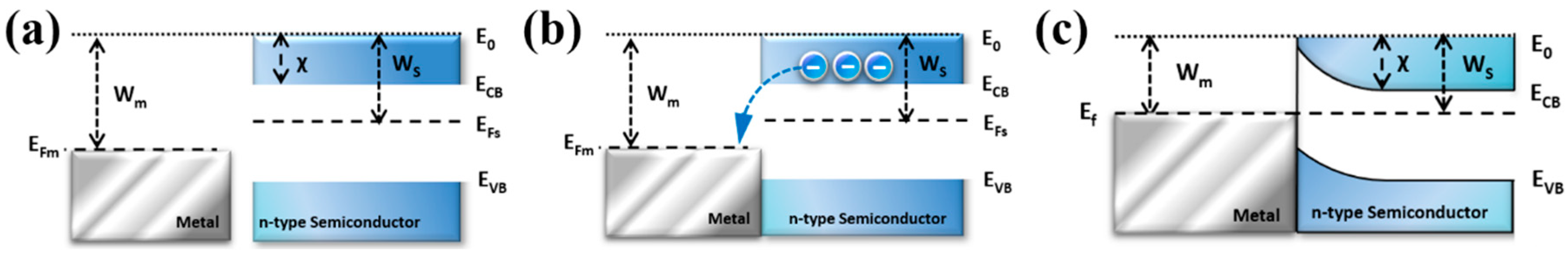
2.1. Formation of Plasmon-Mediated Heterostructure Based on Schottky Contact

The plasmon-mediated heterostructure (PMH) is a kind of composite structure that is constructed with plasmonic metal (gold, silver, and copper) and a semiconductor (conventionally, TiO2, ZnO, Fe2O3 and WO3, as well as new merged BiVO4 and g-C3N4) in nanoscale [34,35,36]. In such a heterostructure, the distinctive feature is the formation of the Schokkty barrier at the interface, which is usually used for regulating the behaviors of HCs. We set an n-type semiconductor as an example and assume that the work function of metal is higher than that of the semiconductor, Wm > Ws (Figure 1a). After they come into contact, there is a tendency for the electrons of the semiconductor to flow into the metal due to the higher Fermi level of the semiconductor than the metal (Figure 1b). The flowing of electrons will not proceed until the formation of a new balance of the Fermi level, namely EF. In the band diagram, the band of the n-type-semiconductor will bend downwards, as seen in Figure 1c. At the moment, the space-charge region with no free electrons is formed and built-in the electric field, and points from the semiconductor to the metal. In this region, the strength of the electric field builds up a high resistance region so that the electrons must have enough energy to get across this region, or barriers in other words, which is defined as the Schottky barrier (φB) [37,38].
The height of the Schottky barrier determines the capacity of electrons to get across. It can be described as:
φ B = W m χ s
where χs is the electron affinity of the semiconductor (equal to E0ECB), and it represents the semiconductor’s ability of accumulating electrons. The height of the barrier can be adjusted in two ways: (1) choose the plasmonic metals with a relatively lower work function [39], such as Ag (4.5–4.7 eV), rather than Au (5.3–5.5 eV); and (2) a higher electron affinity of the semiconductor, which is TiO2 in some works [40].

2.2. Process of Photocatalysis

The typical photocatalytic process based on PMH contains three steps [41], (1) reactants transfer to the surface of photocatalysts, and then reach the adsorption-desorption equilibrium dynamically, (2) light absorption for both the plasmonic metal and semiconductor, after which HCs are generated, (3) transportation of HCs, and the surface redox reaction with O2 and H2O in the surroundings; after formatting the hydroxyl radical and superoxide radical, the decomposition process of the environmental pollutants finally takes place. In this way, there are two key factors that contribute to the efficient photocatalysis: how to increase (1) the ability for the absorption and conversion of photons and (2) the transfer efficiency of HCs. To realize this, the intrinsic nature of HCs needs be understood thoroughly, and the physical model of behaviors of HCs in the process of generation, separation and injection should be established clearly. All these are introduced as follows.

2.2.1. The Generation of HCs

There are two primary processes for the generation of HCs: the excitation of SPs and conversion of photons. In the first process [41], SPs are excited on plasmonic metal with a matched incident light, and at this moment the optical cross sections of the absorption and scatter reach a maximum under an intense interaction between plasmonic metal and the external EM field. Then, the photons, coupled to the plasmonic metal, will dissipate their energy into two forms: re-emitted photons in the radiative transition and a conversion to HCs via the non-radiative transition (Figure 2a). The ratio for generating HCs is in direct proportion to the process of absorption, which means that the effect of the scatter on the re-emission of photons should be suppressed. Furthermore, the character of absorption can be adjusted by the composition, size and shape of the plasmonic metal.
After the light absorption, there are two distinct ways for electrons to transition in plasmonic metals: interband transitions and intraband transitions [42,43], which are the main components of HCs (Figure 2b). In the interband transitions, electrons are excited from the filled d band below the EF to empty the sp band above the EF, and they are insensitive to the shape and size of the metal, as well as to the polarization of the EM field. These transitions are dependent on the location of the d state, which is usually related to the component of the plasmonic metal. For example, the electrons from the d band of gold and copper can be excited by the energy of photons in the visible range, in contrast to silver with a deeper location of the d band [44]. In another electronic transition, the intraband transition, electrons come from the filled s band near the EF to empty the sp band above the EF, and they cannot be excited directly, which results from the non-conservation of momentum. Furthermore, they need an extra momentum to be excited effectively, such as SPs [45]. These plasmon-mediated HCs are more energetic, and their behaviors can be adjusted by designing a specific morphology of the plasmonic metal, especially for anisotropic structures with sharp tips. Additionally, the ways to regulate these parts of HCs are highlighted in this review.

2.2.2. Carriers Separation

As described in Section 2.1., interfacial Schottky barrier is built for the efficient HCs separation, to reduce the probability of are combination of HCs. The behaviors of HCs that reach the interface are as follows [42]: (1) blocked by Schottky barriers, (2) overcoming the Schottky barrier and (3) the tunneling effects. In most works, the third approach, electron tunneling effects, is often neglected for the extreme low possibility of tunneling resulting from a broad charge depletion layer at the interface. The interfacial doping of metal ions is considered an effective way for enhancing the electron tunneling possibility [46,47]. For example, improving the concentrations of doped Ti4+ at the interface of Au/TiO2 can create a narrower depletion layer due to the neutralization reaction with negative charges of Au [47]. In such cases, the electron tunneling effects are remarkably enhanced, and the electrons with a lower energy can pass through without considering the influence of the Schottky barrier.
In addition, the life of HCs is extremely short (hundreds of femtoseconds) and is finally dissipated into heat over a certain period of time (the scale of a picosecond) [27,31]. Their fast injection is of equal important for an efficient utilization. Up to now, there have been two types of mechanisms for HCs separations: one is the classical mechanism that is used for most photocatalysis, a plasmon induced hot-electron transfer (PHET) (Figure 2c) [48,49,50]. In such a system, the behaviors of HCs experience a complex process, including the decay of SPs to generate HCs, transportation, interfacial separation and injection. Within this process, in order to efficiently utilize the HCs before they release their energy to the surroundings, it is crucial to elaborately engineer both the metal and semiconductor. It has been reported that the utilization efficiency of HCs (QY) can be calculated by following Fowler’s equation [51,52]:
Q Y ( ω ) = ( ω φ B ) 2 / ( 4 E F ω )
where ℏω is the energy of the excitation photons. From this, the improvement of QY can be carried out in two aspects: (1) the maximum absorption of solar energy and (2) the reduction of the interfacial barrier. In other words, the QY is related to the efficiency of both the generation and extraction of HCs.
Moreover, an alternative direct electron transfer mechanism was proposed by Lian and colleagues [53], named the plasmon induced metal-to-semiconductor interfacial charge transfer transition (PICTT) (Figure 2d). In this process, the electrons are excited directly to the conduction of the semiconductor with a hole left in the metal, led by strong interdomain coupling effects of the electronic levels. Compared to PHET, the transfer process of HCs is shortened and simplified, which is thought to be much more effective for the utilization of HCs, but the internal physical mechanisms still need to be revealed with deep insight.

2.2.3. Surface Reactions

After the separation of HCs by the Schokkty barrier, the generated HCs will diffuse to the surface of the metal and semiconductor, both induced by the internal EM field to participate in a further chemical reaction. The electrons accumulated in the conduction band of the semiconductor will combine with oxygen to form a superoxide radical for the oxidizing reaction, and the holes left in the metal will participate in a reduction reaction by incorporating with water to convert into a hydroxyl radical (Figure 2e). The specific reaction process is as follows (we set the process of degradation of environmental pollutants as an example):
h V B + + H 2 O H + + H O
e C B + O 2 O 2
P o l l u t a n t + O 2 H 2 O + C O 2 + o t h e r   p r o d u c t s
P o l l u t a n t + H O H 2 O + C O 2 + o t h e r   p r o d u c t s

3. Structural Design of Plasmon-Mediated Photocatalysts

As described above, the behaviors of HCs are sensitive to a specific structural construction, and all of these can be controlled with the strategies of the rational design and optimization of PMH used for high efficiency photocatalysts. Furthermore, we intend to classify the research on the utilization efficiency improvement of HCs into two aspects: (1) the generation of HCs and (2) the ways for them to be extracted by an adjacent semiconductor.

3.1. Generating Efficiency Improvement of HCs

In this subsection, we have introduced the methods for improving the generating efficiency of HCs in several ways, including a “hot spots” structure, broadband absorptive structures made by a plasmonic cavity, and special hollow structures.

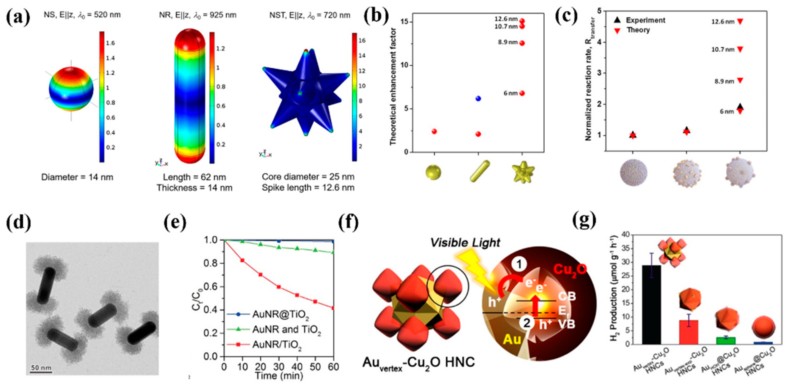
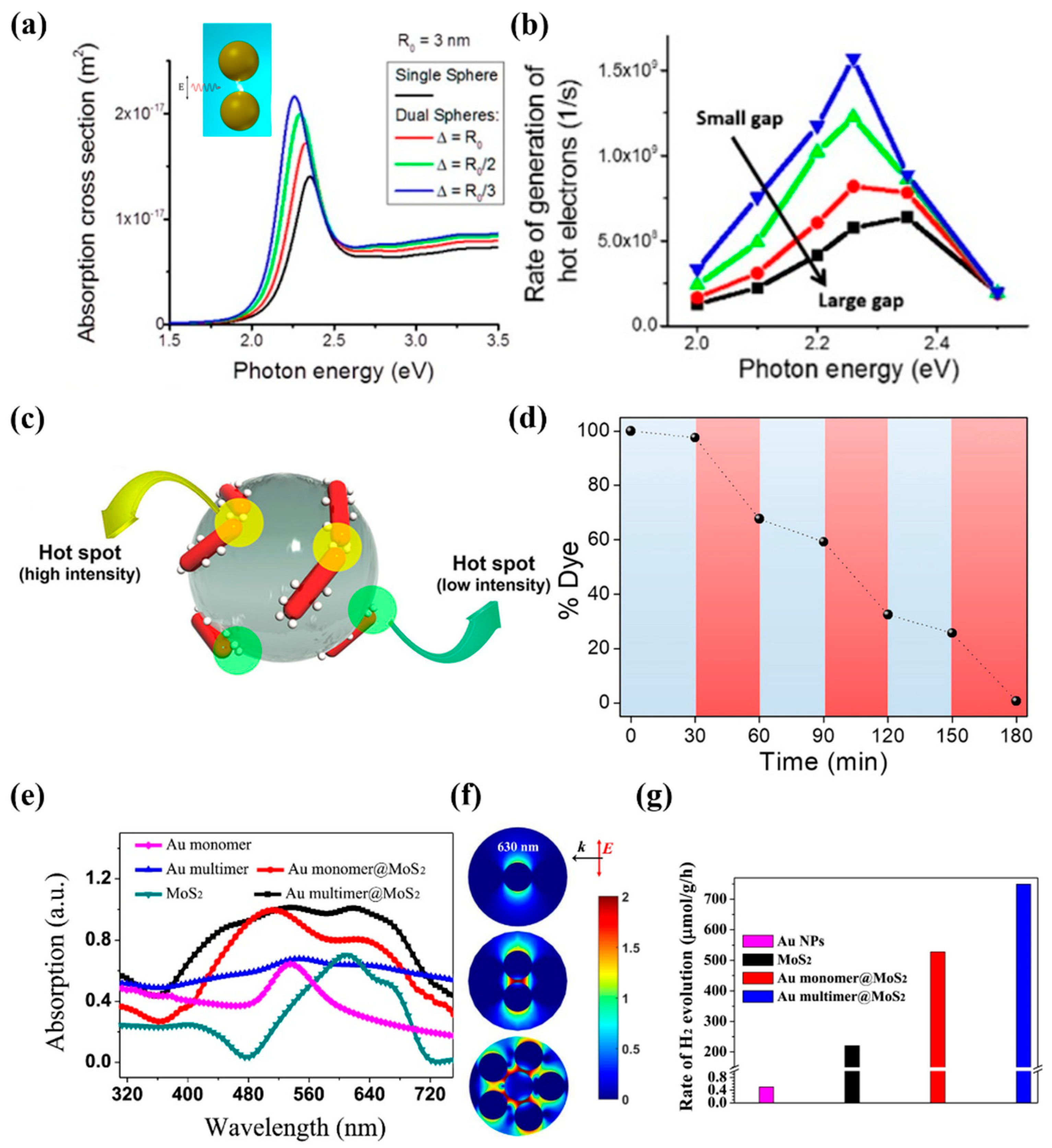
3.1.1. Design of Structures with “Hot Spots”

Recently, it has been shown that the plasmonic metals with “hot spots”, where the EM fields are strongly amplified in small regions, can boost the rates of generation of HCs [54,55,56,57]. Furthermore, this is attributed to two physical reasons [58]: (1) the enhancement of local EM fields in classical effects and (2) the non-conservation of the linear momentum of electrons in quantum formalism. In recent reports, the relations between the rates of generation of HCs and local EM fields were established as follows [59,60]:
R a t e h i g h e n e r g y , ε > Δ E b = 2 π 2 × e 2 E F 2 ω Δ E b ( ω ) 4 S N C | E n o r m a l ( θ , φ ) | 2 d s
where Δ E b is the height of the interfacial barrier, and E n o r m a l ( θ , φ ) is the normal component of the EM fields near the surface. In this equation, the rate of generation of HCs is proportional to the square of the amplitudes of the local EM field in plasmonic metal. In one way, the plasmonic metals with sharp tips or corners (namely “tip hot spots”) [61,62], e.g., nanorods, nanotriangles, and nanocubes, nanostars, are usually designed to be efficient carriers for generating HCs. In such structures, the redistributed electrons are localized near the tips of the metal by perturbing the incident light fields, resulting in several orders of enhancement of the local EM fields. Correa-Duarte et al. [63] studied the morphology-related generation of HCs by setting up three types of plasmonic metals, nanospheres, nanorods and nanostars, as models (Figure 3a). They proposed that plasmonic metals with tip structures (nanorods and nanostars) were endowed with a higher EM field enhancement when compared to nanospheres, and that the structures with long tips contributed to the highest EM enhancement (see the calculated EM enhancement factor in Figure 3b). To build up relations between this EM field enhancement and HCs effects, they assembled plasmonic metals and TiO2 on SiO2 microspheres. Both the theory and the experiments on the catalytic decomposition of RhB indicated that the EM field played a dominant role in the higher generation of HCs (Figure 3c). Such features were also demonstrated in some experimental results. Stucky et al. [64] reported Au-TiO2 dumbbells by fixing amorphous TiO2 at both ends of Au rods (Figure 3d), differing from Au rods@TiO2 and Au rods/TiO2 by simple mixing; the rates of degradation of methyl blue (MB) in these “hot spots” mediated heterostructures were improved significantly (Figure 3e). Han et al. [65] placed the Cu2O at the corners of the Au nanocubes (Figure 3f). This site-selective configuration exhibited an 8.1-fold increment in the photocatalytic hydrogen production compared to the Au@Cu2O core shell nanostructures (Figure 3g).
Another effective way for achieving enhanced EM fields is to design gap “hot spots” structures by arranging the numbers of metallic units rationally. In such an integrating system, the EM fields are localized at the gap between the two or more units, and this globe field enhancement comes from coupling effects in the interaction of the modes of SPs, consequently resulting in a large absorption cross section [66,67,68]. It has been reported that the amplitudes of such EM enhancements are mainly related to the space of the gap and numbers of plasmonic metallic units. Besteiro et al. [69] calculated the characters of optical absorption in metallic nanodimers with different gap spaces. Furthermore, they concluded that the absorption cross section could be increased with narrower gaps (Figure 4a), which then promoted higher rates for generating HCs (Figure 4b). Similarly, Correa-Duarte et al. [70] loaded Au rods-TiO2 on the thermo-responsive polymer and controlled such gap “hot spots” structures dynamically by shrinking or expanding this substrate, mediated by variations of the temperature (Figure 4c). In an experiment of dye decomposition, they demonstrated the improvement of the rates for degrading RhB, which resulted from “hot spots” effects, in which the temperature, when increased to 40 °C, was more effective than in the case of 25 °C (red region for 40 °C and blue region for 25 °C in Figure 4d). Wei et al. [71] investigated the factor of numbers of metallic units in Au@MOS2 structures; both the results in the simulation and the absorption spectrum have shown that more units would bring the localization and enhancement of the intense EM field, followed by extended ranges of photons trapping (Figure 4e,f). Based on this, near 2.4-fold improvements were realized in the photocatalytic hydrogen production by embedding Au multimers in MoS2, compared to pure MoS2 (Figure 4g).

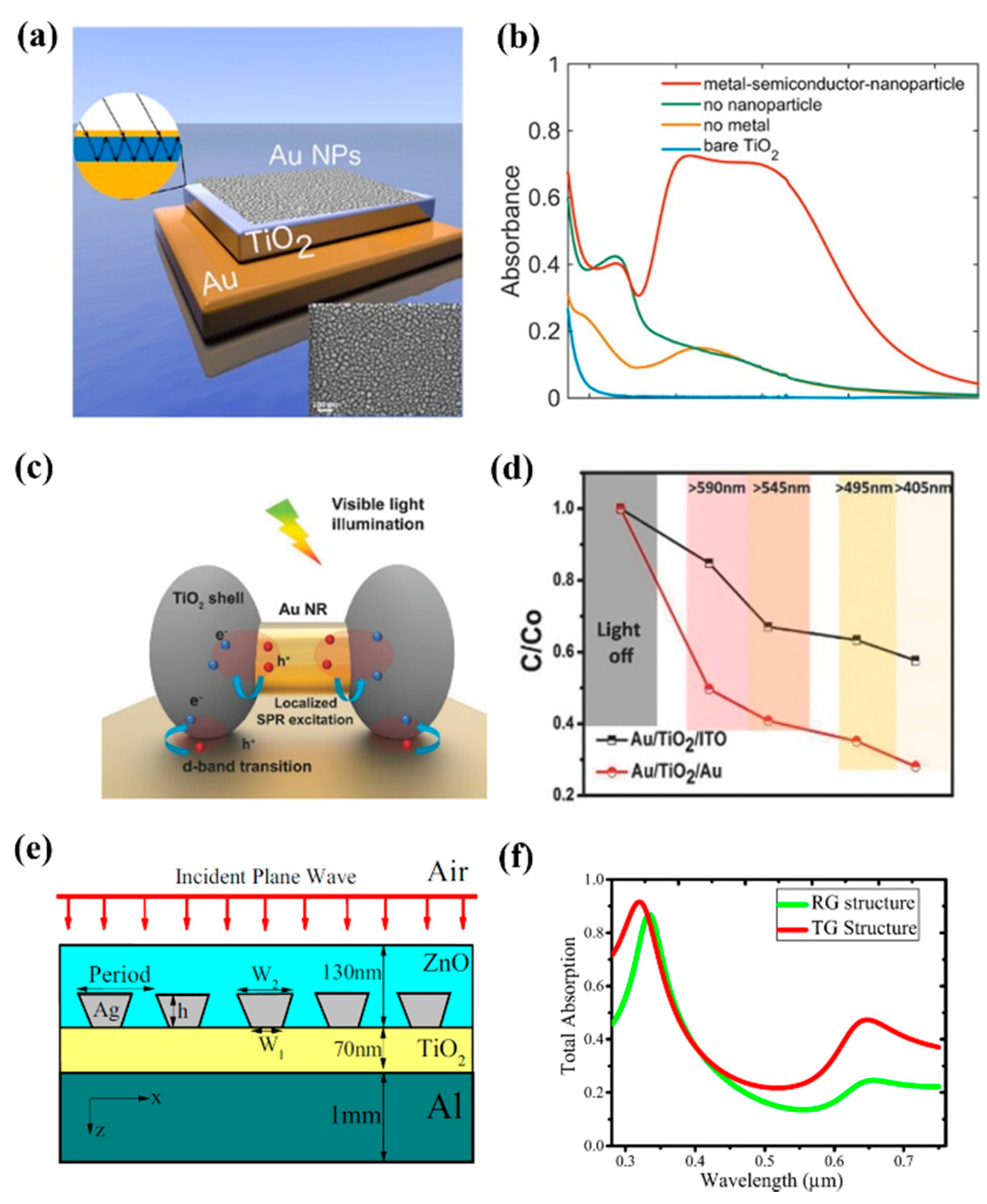
3.1.2. Plasmonic Cavity for Efficient Photons Trapping

To solve the limit of insufficient light absorption, another type of broadband absorption system, plasmonic absorbers-spacer-mirror (ASM), is also taken into consideration [72,73]. Ng et al. [74] proposed Au NPs-TiO2-Au mirrors structures by successively depositing thick Au films, TiO2 layers and packed Au NPs with a certain range of sizes (Figure 5a). Additionally, they explained that the improved photon harvesting ability was rooted in plasmonic Fabry-Perrot (FP) cavity modes, in which incident photons were reflected and scattered between the Au NPs and Au mirror (see inset in Figure 5a). Therefore, the generating efficiency of photons was improved (near 40-fold compared to TiO2/Au NPs) and showed a broad absorption band in the spectrum from 400 nm to 1200 nm (Figure 5b). On the other hand, Lei et al. [75] reported a plasmonic particles-on-film nanocavity by assembling Au nanorods-TiO2 dumbbells on the Au films (Figure 5c). In the process of visible catalytic reactions, the enhancement of the degradation of MB via the integration with Au film, when compared to that of ITO, was attributed to the synergistic effect of d-band electrons transitioning from Au films and SPs induced sp-band electrons transitioning from Au rods, in which SPs induced HCs are dominant at longer wavelengths (>550 nm) and the effects of d-band electrons are emphasized at shorter light excitations (<550 nm) (Figure 5d).
The plasmonic absorbers described above were concentrated on the plasmonic metals with a small size based on localized surface plasmon resonance (LSPR). In recent works, it has been reported that surface plasmon polaritons (SPPs), which travel along the surface of the metallic waveguide structure, are also an efficient medium for the efficient photons conversion by constructing patterned metal structures [76,77]. Rahimi et al. [78] proposed 3D tandem structures consisting of period Ag gratings, a TiO2 layer and Al films (from top to bottom) (Figure 5e). In this way, the Ag gratings on the top layer acted as optical antennas for focusing incident light and as sources for generating HCs when in contact with the TiO2 layer, based on the LSPR and SPPs effects, respectively. To acquire optimal light absorptive structures, they investigated two types of Ag gratings by changing W1 and W2, the rectangular gratings (RG) and trapezoidal gratings (TG). Furthermore, they found that TG based structures had a greater capacity to trap photons compared to other shapes, which was attributed to a lower reflection of TG resulting from the generating gradient in the effective refractive index (Figure 5f). Such SPPs induced structures are much more steerable in their optical character by simply adjusting the light absorption layer, and they are useful for designing angles-dependent photocatalytic applications [79].

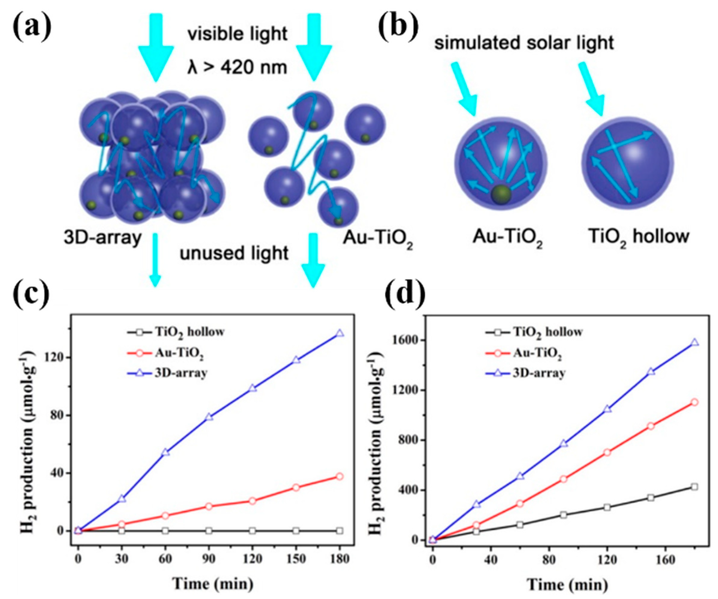
3.1.3. Hollow Heterostructure Designing

In conventional PMH, both the plasmonic metal and semiconductor are usually solid, and the chemical reactions only take place on the outside surface. In such typical structures, most of the photons are missed due to the small interactional area between the light and heterostructures. In addition, the effects of scatter and reflections brought by heterostructures themselves also inevitably waste photons. The proposed hollow structures can solve this problem, and they have been attracting much attention for their high utilization of photons [80,81]. Majima et al. [82] reported an Au@TiO2 hollow heterostructure and proposed that the Au core in hollow TiO2 served as an effective scattering center, increasing the degrees of reflection of the light and optical path (Figure 6a,b). Therefore, the scattered or reflected photons are re-utilized by the catalyst and promote the generation of HCs. This special effect is called the slow-photon effect, with which the absorption of photons are improved dramatically at the absorption range of the catalyst [83]. Furthermore, they also found that the ordered 3D arrays constructed by this heterostructure are much more efficient for the H2 generation when compared to random ones (Figure 6c,d). The enhancement of the activity in ordered 3D arrayed structures was ascribed as being “cavity” effects that were constructed by the rational arrangement of the unit of Au-TiO2. In this special cavity, light was regulated by building up oriented photons transporting channels, in which the recombination of HCs that occurred in adjoining units is suppressed via the migration of HCs [84]. Apart from the re-utilization of photons, the fast separation of HCs is another superior advantage; the generated HCs are separated and transported to the inner and outer surface simultaneously [85]. In this way, the recombination of HCs resulting from the long transporting distance can be avoided, which thus speeds up the reaction process. Besides, the process of photocatalysis only takes place at the surface of the catalysts, which entails that the enhancement of the activity with a higher specific surface area [86]. Therefore, the addition of an inside surface from hollow structures means that there is a higher opportunity for active atoms to come into contact with more reactants, thus improving the efficiency of catalytic reactions.

3.2. Extraction of HCs

In this section, the methods to efficiently extracting HCs are illustrated based on interfacial band engineering, including an atomically organized interface with less defects, an interfacial post-treatment, the ways to fast separate interficial HCs and the selection of a crystal face. In addition, the external factor, the polarization of light, is also taken into consideration.

3.2.1. Surface and Interfacial Quality Engineering

In quite a few works, it has been found that the abundant defects and interfacial lattice mismatches in heterostructures were difficult to thoroughly avoid, limited by the poor control in the process of chemical synthesis. Furthermore, these defects and mismatches usually served as electron capture bands that trapped the HCs when they were moving in an orientated way [87,88,89]. This process will decrease the amounts of electrons that are injected into the adjacent semiconductor, and their final utilization efficiency is further reduced. To optimize the channel for transferring HCs, it is necessary to elaborately engineer the interfacial states by achieving high quality monocrystalline nanostructures (both for the metal and semiconductor) and smooth interfacial regions [90,91]. Zhang et al. [92] proposed experimentally an aqueous cation exchange method for preparing Au@MS (M = Cd, Zn) with atomically organized interfaces (Figure 7a). A transient absorption spectroscopy measurement showed the strongest signals of these high quality structures compared to Au and Au@MS, based on conventional methods (Figure 7b). In such a process, the avoidance of non-conduction binding ligands and the mild interfacial transition made them a “soft” contact, where the interfacial defects were reduced dramatically by reorganizing the lattice structure; the calculated efficiency of the injection of HCs was raised to ~48%. Similarly, Chang et al. [93] compared the thickness of shell matters for the decomposition of MB by using this kind of method (Figure 7c). Additionally, they demonstrated that these core-shell type heterostructures with a thinner shell were efficient in degrading the MB due to the limited diffusion length of the HCs (Figure 7d).
In addition, by constituting a chemical bond, the insulating organic ligands used for binding the metal and semiconductor is another hindrance for electron transfers [94,95]. Therefore, a post-treatment process for efficiently removing non-conducting macromolecular materials, such as polyvinyl pyrrolidone (PVP), hexadecyl trimethyl ammonium bromide (CTAB), etc., is of considerable importance for the effective transfer and injection of HCs moving to the interface [96,97,98,99,100]. Yin et al. [96] reported a ligand-exchange method combined with a mild thermal post-treatment for effectively removing insulating ligands (PVP) in Au-TiO2 heterostructures (Figure 8a). In their work, the original PVP was replaced by mercaptopropionic acid (MPA) for their higher affinity to Au. Then, they removed MPA completely by low-temperature annealing (200 °C). The efficiency of dye decompositions was improved significantly due to the tight formation of the Schottky contact and the maintenance of the original morphology compared to conventional deposition-decomposition methods and samples without any treatment (Figure 8b). An alternative way, the solvent extraction procedures, was brought into focus as well. Hutchings et al. [97] proposed a water extraction method to remove the excess polyvinyl alcohol (PVA) which served as stabilizing agent in Au/TiO2 under a mild ambient. In this process, the contents of PVA were reduced gradually under different refluxing times (Figure 8c). Additionally, compared to conventional high-temperature calcination, the oxidation ability of CO was demonstrated to be highly effective due to Au/TiO2 keeping its original morphology (Figure 8d).

3.2.2. Efficient Separation of Interfacial HCs

In PMH, the recombination of electron-hole pairs cannot be thoroughly avoided due to short pathways for transferring charges and due to the relatively high interfacial potential barrier. The rational design of the potential gradient between plasmonic metals and the semiconductor is an efficient way for reducing potential differences and inducing the controllable transporting of HCs [101,102,103,104]. Based on this, Chen et al. [101] reported TiO2 nanotube-Al2O3-Au ternary structures for the efficient separation of HCs excited by Au nanospheres (Figure 9a). In such structures, the formation of an electron depletion layer at the interface of TiO2 and Al2O3 served as an effective channel for the transportation of HCs and thus suppressed the HCs recombination (Figure 9b). Besides, another issue needs to be considered: the recombination of HCs resulting from adjacent structures. Tachikawa et al. [102] proposed that the hindrance of HCs transferring and fast recombination usually took place in a conventional hybrid system, and they optimized this by constructing ordered structures (Au/MesoTiO2) to realize controllable movements of HCs. In such structures, HCs were guided in a constant direction, so that the unnecessary recombination of charges would be avoided (Figure 9c). Based on this, the rates of degradation of MB were improved remarkably when compared to other non-ordered systems (Figure 9d). The time-resolved transient absorption spectrum showed that this Au/MesoTiO2 possessed the slowest decay of HCs’ life, which gave direct evidence of the retarding effects of the recombination of HCs (Figure 9e).

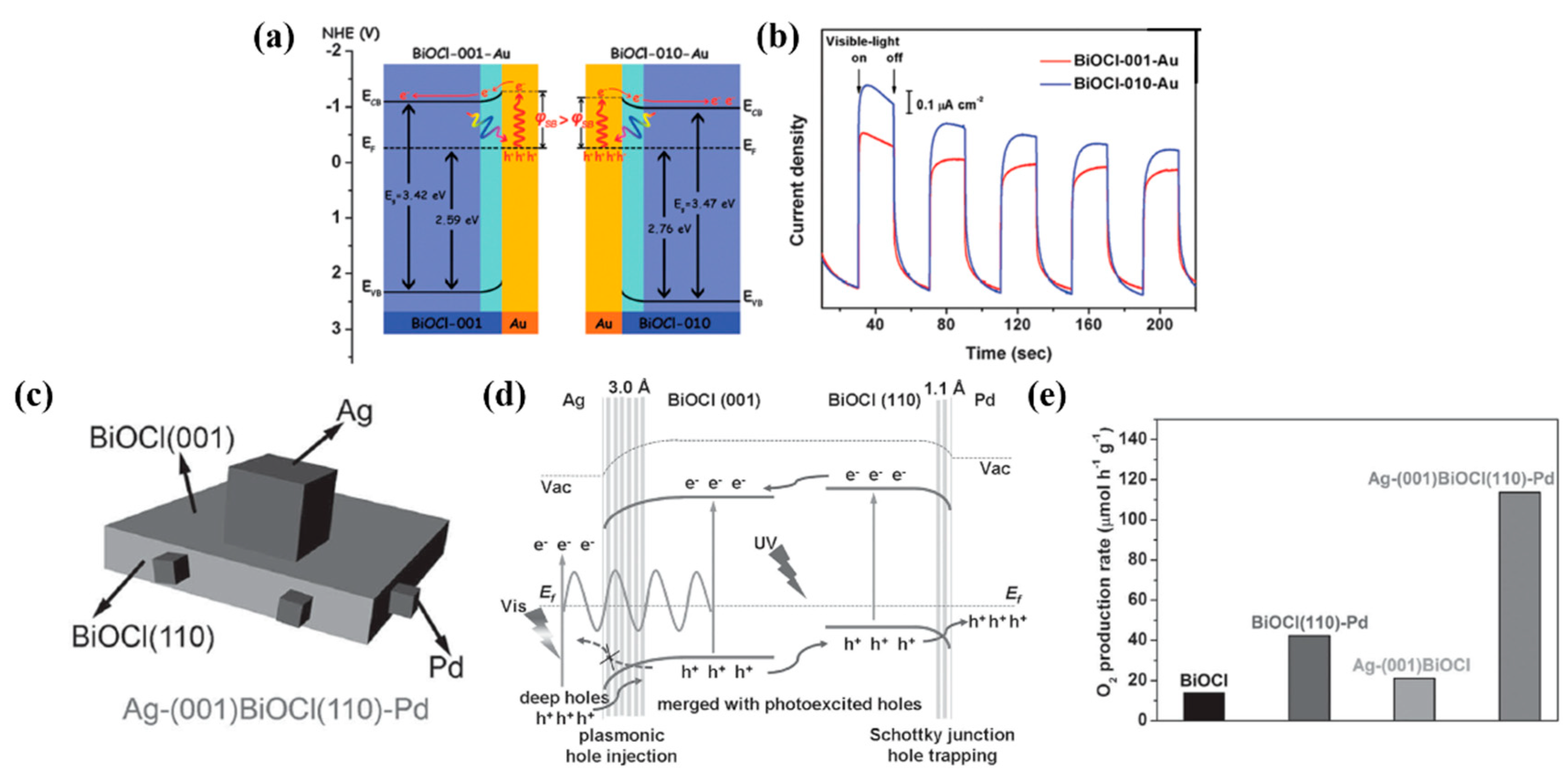
3.2.3. Crystal Orientation

In some works, it has been found that the transferring of HCs can also be modulated by choosing a specific point of contact of the crystal face between the plasmonic metal and semiconductor [105,106,107]. In this way, the preferential accumulation and transfer of HCs with proper band positions will reduce the height of the interfacial barriers, and hence more HCs can get across. Ye et al. [105] reported that the efficiency in the degradation of 2-propanol in BiOCl-010-Au was 3.5-fold higher than for another type of contact, BiOCl-001-Au. They attributed this phenomenon to the lower degree of interfacial band bending in Au-BiOCl-010 than in Au-BiOCl-001, which led to more HCs getting across the Schottky barrier and then being utilized by adjacent BiOCl (Figure 10a). Furthermore, this was verified in the measurement of the current density intensity in BiOCl-001-Au and BiOCl-010-Au (Figure 10b). Furthermore, to control the flow and separate HCs efficiently, Xiong et al. [106] integrated Ag and Pd at the BiOCl (001) and BiOCl (110), respectively (Figure 10c). The synergistic effect of both the HCs injection and Schottky junctions exhibits a threefold enhancement of the photocatalytic oxygen production compared to single BiOCl, BiOCl (110)-Pd, and Ag-(001) BiOCl (Figure 10d,e).

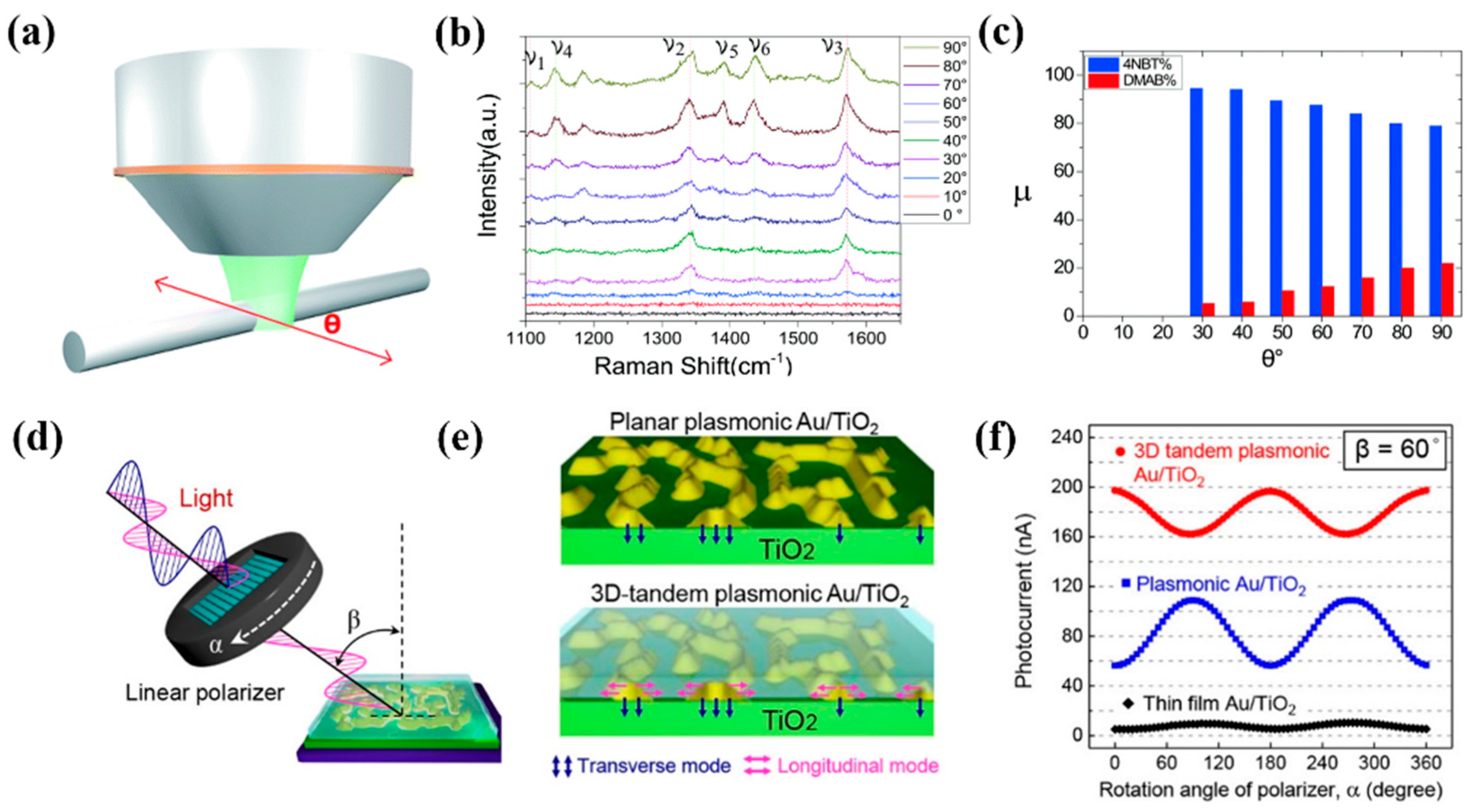
3.2.4. Optic Field Distribution Consideration

An additional feature for SPs is their dependence on the external incident EM field, which means that the traveling of HCs can be adjusted by choosing different polarizations of light [108,109,110,111,112]. Wang et al. [108] investigated the transferring of HCs at different angles of the polarization of incident light on the single silver nanowire combined with 4-nitrobenzenethiol (4NBT) (Figure 11a). The enhancement of Raman peaks in 4NBT (Figure 11b) and the increasing coverage of p, p′-dimercaptoazobenzene (DMAB) reduced by 4NBT (Figure 11c) have both indicated that there were more generated HCs transferring to the interface of the Ag nanowire and 4NBT. Furthermore, this polarization-dependent phenomenon is also obvious in 2D and 3D hybrid structures. Park et al. [109] investigated the behaviors of HCs under two types of polarized light, the longitudinal mode and transverse mode, in 2D and 3D Au/TiO2 heterostructures, respectively (Figure 11d). In Figure 11f, both the 2D and 3D structures exhibited different responses of HCs transportation, and the 3D structures were more effective than the 2D ones, due to the multi-dimensional transfer of HCs (Figure 11e). Particularly, the extracting efficiency of HCs will reach a maximum when the HCs’ momentum is perpendicular to the Schottky interface.

4. Applications of Plasmonic Photocatalysts in Environmental Protection

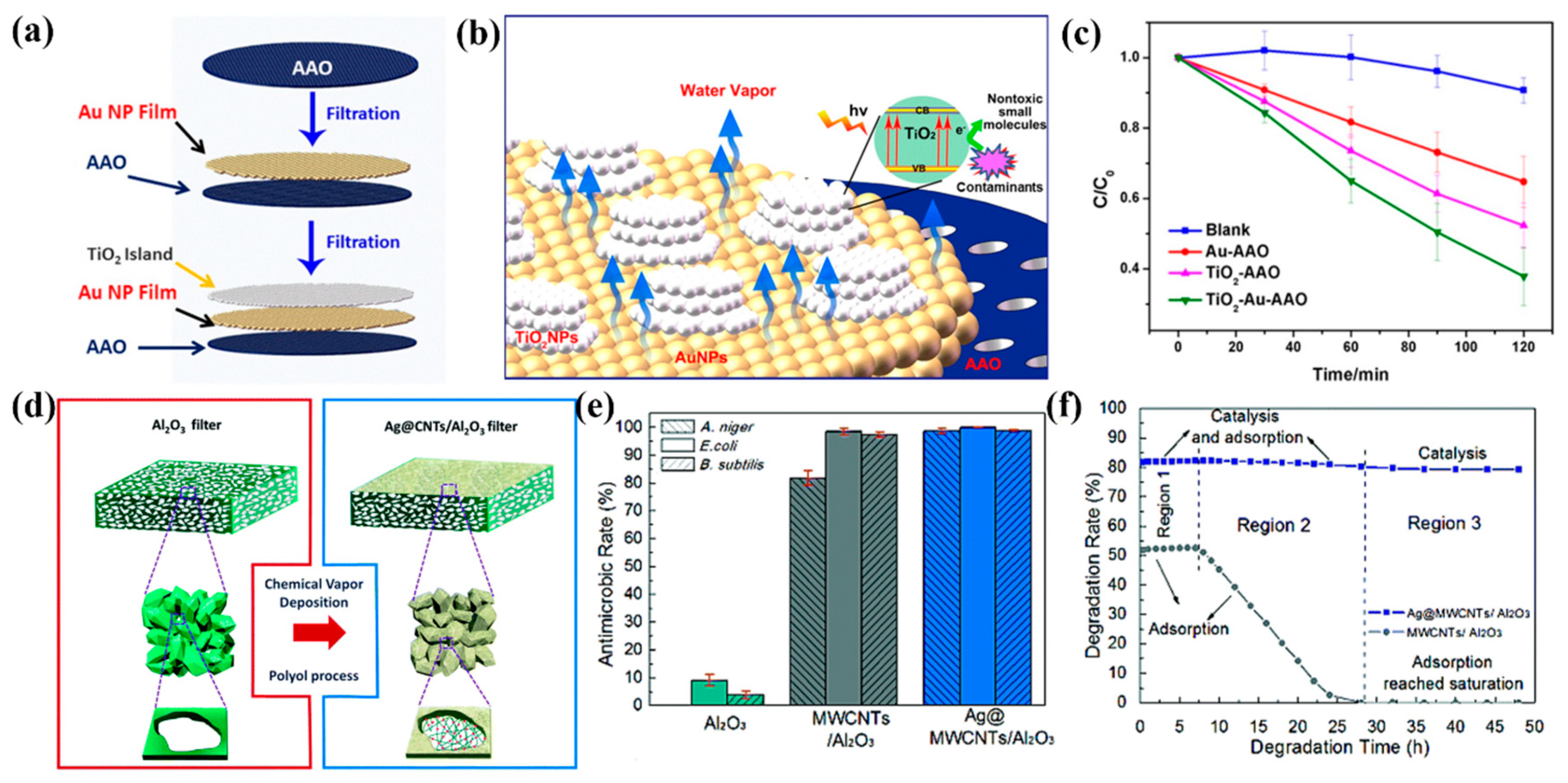
4.1. Water Treatment

In recent years, membrane based visible response heterostructural catalysts for multi-functions have been reported for high efficiency and broad-spectrum environmental pollutants purifications. The combination of membrane and plasmon based photocatalysts can reduce the “secondary pollution” resulting from the leakage of the catalyst itself and can also lower the cost. For example, an emerging technology, seawater desalination and catalysis, combined with plasmonic photocatalysts, has paid closer attention to solving the bottlenecks resulting from the shortage of fresh water [113,114,115]. A bifunctional membrane, which contains TiO2 islands, Au films and porous anodized aluminum oxide (AAO) substrate from the top to bottom, was reported for an effective steam generation and pollutants elimination [114] (Figure 12a). In this structure, plasmonic metals act as optical antennae that selectively and effectively absorb the energy of photons in a broad solar spectrum; the synergetic heating effects and HCs effects resulting from decayed HCs will not only speed up the steam generation from seawater, but also boost the rates of decomposition of pollutants with the aid of catalysts (Figure 12b,c).

4.2. Air Purification

Indoor and outdoor air pollutions are also major issues to be addressed for the sake of human health. Typical air pollutants are mainly divided into three aspects, (1) inorganic and organic chemical compound gas, including oxynitride (NO, NO2), oxysulfide (SO2, SO3), toluene and volatile organic compounds (VOCs), (2) pathogens (bacteria, viruses) and (3) suspended particulate matter (PM2.5). Hence, it is necessary to develop multifunctional air purification technology to realize broad-spectrum air pollution treatments [116,117,118]. In recent years, various types of air purification filters made by one-dimensional nanostructure have been made, including metal nanowires [119,120], carbon based-materials [121] and polymer nanofibers [122,123], due to their high active surface areas, mechanical stability and functionalization. Furthermore, they are effective in various air pollutant purifications by being combined with PMH. Figure 12d shows a multilayers air purification filter based on hierarchical Ag@MWCNTs/porous Al2O3 [124]. In such structures, the network like distribution of Ag@MWCNTs placed at the pores of Al2O3 serves as an effective medium for catalytic reactions. Compared to Al2O3, Ag@MWCNTs and MWCNTs/Al2O3, the large active surface area, high catalyst mediated by plasmonic Ag and retention of particles, without decreasing the air pressure drop significantly, resulted from these hierarchical structures, and a highly efficient elimination of VOCs and aerosol microorganisms was achieved simultaneously (Figure 12e,f).
Apart from the above, “Greenhouse Effects” mediated by high-ratio CO2 in air cannot be neglected, and the question of how to solve this critical problem is also a hot topic in modern society. A good deal of studies, combined with PMH photocatalysts, have been reported for the effective reduction of CO2 from different point of views, including light absorption, the separation and diffusion of carriers and the activated adsorption of reactants [125,126]. Based on this, the rational designing routes [127,128], such as doping, alloying, band engineering, lattice control, introduced defects, and so on, are raised for the reduction and conversion of CO2 into new fuels (methane, methanol and formic acid), which in practice is deemed to be of great value.

4.3. Photochemical Reactions

PMH photocatalysts are also explored for photochemical reactions, such as organic transformations, having a low toxicity and being environmental [129,130]. At present, the involved organic transformations mediated by PMH photocatalysts can be summarized into mainly three aspects [131,132,133]: (1) the oxidation of alcohol, amine, alkene and alkane or hydroxylation reactions of aromatic compounds, (2) the activation and functionalization of α-C-H bonds to build up C-C bonds or C-X (X = O, N or S) bonds and (3) the reduction of nitrobenzene to aminobenzene or azobenzene. Compared to conventional routes, PMH photocatalysts can bring milder reaction conditions that are derived from light in contrast to heat-induced chemical reactions; most reactions can be achieved under room temperature or even lower. The carriers can be controlled by a rational design of band structures that will both stimulate the rates and shorten the period of chemical reactions. All of these have promising perspectives for the elaborate fabrication of organic compounds, such as medicine and spice.

5. Conclusions and Perspectives

In the past several years, with the development of advanced materials and microscopy, substantial progress has been realized to make deep insights into the kinetics of HCs in PMH based photocatalysts. The efforts for the design of high-performance PMH, including the compositions, morphology, and band structures between metals and semiconductors and the external EM field, have been sufficiently developed for the effective harvesting and transferring of photons. In this review, we presented the progress in the rational design of photocatalysts based on PMH in recent years. The “hot spots” structures, plasmonic cavity and hollow structures for obtaining photon trapping in a broad spectrum are introduced. To realize a fast transfer of HCs, some reliable methods, including clearer interfacial regions, the rational design of electrical transporting channel, a specific contact of the crystal face and the polarization of incident light, are individually detailed. In addition, the typical applications for environmental protections are also listed in order to give a brief framework for researchers to focus on in the present.
There are also some points to consider for future investigations. First, the exact physical model for the process relating to the generation, transportation and injections of HCs needs to be built up. There are arguments that the dominating contributions of electrons (interband transitions with a relatively low energy of electrons or intraband transitions induced by SPs) from photoexcited metals is the improvement of catalytic reactivity, and some works have given different opinions [134,135]. The distinguishing of non-thermal effects (HCs effects) and thermal effects, which allows us to quantify each contribution for the enhancement of the process of photocatalysis, is also of great importance for designing specific structures with different purposes [136,137,138]. Second, in the past years, although numerable technologies on the optimization and design of the rational employment of PMH have emerged [139,140,141,142,143], the crystal growth mechanisms and hetero-assembly techniques still need to be revealed clearly. Furthermore, the optical characteristics of PMH are studied mainly on a macroscopic level; for example, the absorption and reflection in self-assembly films, and the optical phenomena we observed, are integrated effects with millions of nanostructures. Additionally, the microscopic evidence of a single structure must be presented urgently for a comprehensive understanding of light-matter interactions [144,145,146]. In this regard, the in situ characterization technique must be further developed to help solve these limits. Practically, for rich functional systems, the cost, biocompatibility, stability and ease to integrate into other platforms must also be considered.

Author Contributions

T.Z. and S.-J.W. drafted the main parts of manuscript. X.-Y.Z., D.S., Y.Y., J.-Y.W., Y.-Y.X. and N.Z. participated in the draft preparation. All authors read and approved the final manuscript.

Funding

This research was funded by MOST under grant number 2017YFA0205800, NSFC under grant numbers 61875241 and 11734005, the Fundamental Research Funds for the Central Universities, Southeast University under grant number 2242019k1G034.

Conflicts of Interest

The authors declare no conflict of interest.

References

  1. Fujishima, A.; Honda, K. Electrochemical photolysis of water at a semiconductor electrode. Nature 1972, 238, 37–38. [Google Scholar] [CrossRef] [PubMed]
  2. Zou, Z.; Ye, J.; Sayama, K.; Arakawa, H. Direct splitting of water under visible light irradiation with an oxide semiconductor photocatalyst. Nature 2001, 414, 625–627. [Google Scholar] [CrossRef] [PubMed]
  3. Asahi, R.; Morikawa, T.; Ohwaki, T.; Aoki, K.; Taga, Y. Visible-light photocatalysis in nitrogen-doped titanium oxides. Science 2001, 293, 269–271. [Google Scholar] [CrossRef] [PubMed]
  4. Maeda, K.; Teramura, K.; Lu, D.; Takata, T.; Saito, N.; Inoue, Y.; Domen, K. Photocatalyst releasing hydrogen from water. Nature 2006, 440, 295. [Google Scholar] [CrossRef] [PubMed]
  5. Yi, Z.; Ye, J.; Kikugawa, N.; Kako, T.; Ouyang, S.; Stuart-Williams, H.; Yang, H.; Cao, J.; Luo, W.; Li, Z.; et al. An orthophosphate semiconductor with photooxidation properties under visible-light irradiation. Nat. Mater. 2010, 9, 559–564. [Google Scholar] [CrossRef] [PubMed]
  6. Reece, S.Y.; Hamel, J.A.; Sung, K.; Jarvi, T.D.; Esswein, A.J.; Pijpers, J.J.H.; Nocera, D.G. Wireless solar water splitting using silicon-based semiconductors and earth-abundant catalysts. Science 2011, 334, 645–648. [Google Scholar] [CrossRef]
  7. Kumar, S.G.; Devi, L.G. Review on modified TiO2 photocatalysis under UV/visible light: Selected results and related mechanisms on interfacial charge carrier transfer dynamics. J. Phys. Chem. A 2011, 115, 13211–13241. [Google Scholar] [CrossRef]
  8. Qiu, J.; Wei, W.D. Surface plasmon-mediated photothermal chemistry. J. Phys. Chem. C 2014, 118, 20735–20749. [Google Scholar] [CrossRef]
  9. Friedmann, D.; Hakki, A.; Kim, H.; Choi, W.; Bahnemann, D. Heterogeneous photocatalytic organic synthesis: State-of-the-art and future perspectives. Green Chem. 2016, 18, 5391–5411. [Google Scholar] [CrossRef]
  10. Ismail, A.A.; Bahnemann, D.W. Photochemical splitting of water for hydrogen production by photocatalysis: A review. Sol. Energy Mater. Sol. C 2014, 128, 85–101. [Google Scholar] [CrossRef]
  11. Gao, M.; Zhu, L.; Ong, W.L.; Wang, J.; Ho, J.W. Structural design of TiO2-based photocatalyst for H2 production and degradation applications. Catal. Sci. Technol. 2015, 5, 4703–4726. [Google Scholar] [CrossRef]
  12. Chong, M.N.; Jin, B.; Chow, C.W.K.; Saint, C. Recent developments in photocatalytic water treatment technology: A review. Water Res. 2010, 44, 2997–3027. [Google Scholar] [CrossRef]
  13. Di Paola, A.; García-López, E.; Marcì, G.; Palmisano, L. A survey of photocatalytic materials for environmental remediation. J. Hazard. Mater. 2012, 211, 3–29. [Google Scholar] [CrossRef]
  14. Maier, S.A.; Brongersma, M.L.; Kik, P.G.; Meltzer, S.; Requich, A.A.G.; Atwater, H.A. Plasmonics-a route to nanoscale optical devices. Adv. Mater. 2001, 13, 1501–1505. [Google Scholar] [CrossRef]
  15. Maier, S.A. Plasmonics: Metal nanostructures for subwavelength photonic devices. IEEE J. Sel. Top. Quant. 2006, 12, 1214–1220. [Google Scholar] [CrossRef]
  16. Zhang, T.; Su, D.; Li, R.Z.; Wang, S.J.; Shan, F.; Xu, J.J.; Zhang, X.Y. Plasmonic nanostructures for electronic designs of photovoltaic devices: Plasmonic hot-carrier photovoltaic architectures and plasmonic electrode structures. J. Photonics Energy 2016, 6, 042504. [Google Scholar] [CrossRef]
  17. Ingram, D.B.; Linic, S. Water splitting on composite plasmonic-metal/semiconductor photoelectrodes: Evidence for selective plasmon-induced formation of charge carriers near the semiconductor surface. J. Am. Chem. Soc. 2011, 133, 5202–5205. [Google Scholar] [CrossRef]
  18. Kochuveedu, S.T.; Jang, Y.H.; Kim, D.H. A study on the mechanism for the interaction of light with noble metal-metal oxide semiconductor nanostructures for various photophysical applications. Chem. Soc. Rev. 2013, 42, 8467–8493. [Google Scholar] [CrossRef]
  19. Li, J.; Cushing, S.K.; Meng, F.; Senty, T.R.; Bristow, A.D.; Wu, N. Plasmon-induced resonance energy transfer for solar energy conversion. Nat. Photonics 2015, 9, 601–607. [Google Scholar] [CrossRef]
  20. Maier, S.A.; Atwater, H.A. Plasmonics: Localization and guiding of electromagnetic energy in metal/dielectric structures. J. Appl. Phys. 2005, 98. [Google Scholar] [CrossRef]
  21. Liu, Z.; Hou, W.; Pavaskar, P.; Aykol, M.; Cronin, S.B. Plasmon resonant enhancement of photocatalytic water splitting under visible illumination. Nano Lett. 2011, 11, 1111–1116. [Google Scholar] [CrossRef]
  22. Tian, Y.; Tatsuma, T. Plasmoninduced photoelectrochemistry at metal nanoparticles supported on nanoporous TiO2. Chem. Commun. 2004, 1810–1811. [Google Scholar] [CrossRef]
  23. Tian, Y.; Tatsuma, T. Mechanisms and applications of plasmon-induced charge separation at TiO2 films loaded with gold nanoparticles. J. Am. Chem. Soc. 2005, 127, 7632–7637. [Google Scholar] [CrossRef]
  24. Christopher, P.; Moskovits, M. Hot charge carrier transmission from plasmonic nanostructures. Annu. Rev. Phys. Chem. 2017, 68, 379–398. [Google Scholar] [CrossRef]
  25. Zhan, C.; Chen, X.J.; Yi, J.; Li, J.F.; Wu, D.Y.; Tian, Z.Q. From plasmon-enhanced molecular spectroscopy to plasmon-mediated chemical reactions. Nat. Rev. Chem. 2018, 2, 216–230. [Google Scholar] [CrossRef]
  26. Aslam, U.; Rao, V.G.; Chavez, S.; Linic, S. Catalytic conversion of solar to chemical energy on plasmonic metal nanostructures. Nat. Catal. 2018, 1, 656–665. [Google Scholar] [CrossRef]
  27. Brongersma, M.L.; Halas, N.J.; Nordlander, P. Plasmon-induced hot carrier science and technology. Nat. Nanotechnol. 2015, 10, 25–34. [Google Scholar] [CrossRef]
  28. O’Brien, K.; Lanzillotti-Kimura, N.D.; Rho, J.; Suchowski, H.; Yin, X.; Zhang, X. Ultrafast acousto-plasmonic control and sensing in complex nanostructures. Nat. Commun. 2014, 5, 4042. [Google Scholar] [CrossRef]
  29. Subramanian, P.; Meziane, D.; Wojcieszak, R.; Dumeignil, F.; Boukherroub, R.; Szunerits, S. Plasmon-Induced Electrocatalysis with Multi-Component Nanostructures. Materials 2019, 12, 43. [Google Scholar] [CrossRef]
  30. Tan, S.; Argondizzo, A.; Ren, J.; Liu, L.; Zhao, J.; Petek, H. Plasmonic coupling at a metal/semiconductor interface. Nat. Photonics 2017, 11, 806–812. [Google Scholar] [CrossRef]
  31. Cushing, S.K. Plasmonic hot carriers skip out in femtoseconds. Nat. Photonics 2017, 11, 748–749. [Google Scholar] [CrossRef]
  32. Valentine, J. Bridging the gap with hot electrons. Nat. Nanotechnol. 2018, 13, 96–97. [Google Scholar] [CrossRef]
  33. Yu, S.; Wilson, A.J.; Heo, J.; Jain, P.K. Plasmonic control of multi-electron transfer and C–C coupling in visible-light-driven CO2 reduction on Au nanoparticles. Nano Lett. 2018, 18, 2189–2194. [Google Scholar] [CrossRef]
  34. Achermann, M. Exciton-plasmon interactions in metal-semiconductor nanostructures. J. Phys. Chem. Lett. 2010, 1, 2837–2843. [Google Scholar] [CrossRef]
  35. DuChene, J.S.; Sweeny, B.C.; Johnston-Peck, A.C.; Su, D.; Stach, E.A.; Wei, W.D. Prolonged hot electron dynamics in plasmonic-metal/semiconductor heterostructures with implications for solar photocatalysis. Angew. Chem. Int. Edit. 2014, 53, 7887–7891. [Google Scholar] [CrossRef]
  36. Wang, X.; Zhang, C.; Du, J.; Dong, X.; Jian, S.; Yan, L.; Gu, Z.; Zhao, Y. Enhanced Generation of Non-Oxygen Dependent Free Radicals by Schottky-Type Heterostructures of Au-Bi2S3 Nanoparticles via X-Ray-Induced Catalytic Reaction for Radiosensitization. ACS Nano 2019. [Google Scholar] [CrossRef]
  37. Walter, M.G.; Warren, E.L.; McKone, J.R.; Boettcher, S.W.; Mi, Q.X.; Santori, E.A.; Lewis, N.S. Solar water splitting cells. Chem. Rev. 2010, 110, 6446–6473. [Google Scholar] [CrossRef]
  38. Ran, J.; Zhang, J.; Yu, J.; Jaroniec, M.; Qiao, S.Z. Earth-abundant cocatalysts for semiconductor-based photocatalytic water splitting. Chem. Soc. Rev. 2014, 43, 7787–7812. [Google Scholar] [CrossRef]
  39. Nishi, H.; Torimoto, T.; Tatsuma, T. Wavelength-and efficiency-tunable plasmon-induced charge separation by the use of Au–Ag alloy nanoparticles. Phys. Chem. Chem. Phys. 2015, 17, 4042–4046. [Google Scholar] [CrossRef]
  40. Tung, R.T. The physics and chemistry of the Schottky barrier height. Appl. Phys. Rev. 2014, 1, 011304. [Google Scholar] [Green Version]
  41. Fujishima, A.; Zhang, X.; Tryk, D.A. TiO2 photocatalysis and related surface phenomena. Surf. Sci. Rep. 2008, 63, 515–582. [Google Scholar] [CrossRef]
  42. Clavero, C. Plasmon-induced hot-electron generation at nanoparticle/metal-oxide interfaces for photovoltaic and photocatalytic devices. Nat. Photonics 2014, 8, 95–103. [Google Scholar] [CrossRef]
  43. Petek, H.; Nagano, H.; Ogawa, S. Hot-electron dynamics in copper revisited: The d-band effect. Appl. Phys. B Lasers Opt. 1999, 68, 369–375. [Google Scholar] [CrossRef]
  44. Sundararaman, R.; Narang, P.; Jermyn, A.S.; Goddard, W.A.; Atwater, H.A. Theoretical predictions for hot-carrier generation from surface plasmon decay. Nat. Commun. 2014, 5, 5788. [Google Scholar] [CrossRef]
  45. Khurgin, J.B. How to deal with the loss in plasmonics and metamaterials. Nat. Nanotechnol. 2015, 10, 2–6. [Google Scholar] [CrossRef]
  46. Xue, J.; Elbanna, O.; Kim, S.; Fujitsuka, M.; Majima, T. Defect state-induced efficient hot electron transfer in Au nanoparticles/reduced TiO2 mesocrystal photocatalysts. Chem. Commun. 2018, 54, 6052–6055. [Google Scholar] [CrossRef]
  47. Shiraishi, Y.; Yasumoto, N.; Imai, J.; Sakamoto, H.; Tanaka, S.; Ichikawa, S.; Ohtanie, B.; Hiraia, T. Quantum tunneling injection of hot electrons in Au/TiO2 plasmonic photocatalysts. Nanoscale 2017, 9, 8349–8361. [Google Scholar] [CrossRef]
  48. Sönnichsen, C.; Franzl, T.; Wilk, T.; von Plessen, G.; Feldmann, J.; Wilson, O.; Mulvaney, P. Drastic reduction of plasmon damping in gold nanorods. Phys. Rev. Lett. 2002, 88, 077402. [Google Scholar] [CrossRef]
  49. Hartland, G.V. Optical studies of dynamics in noble metal nanostructures. Chem. Rev. 2011, 111, 3858–3887. [Google Scholar] [CrossRef]
  50. Govorov, A.O.; Zhang, H.; Gun’ko, Y.K. Theory of photoinjection of hot plasmonic carriers from metal nanostructures into semiconductors and surface molecules. J. Phys. Chem. C 2013, 117, 16616–16631. [Google Scholar] [CrossRef]
  51. Fowler, R.H. The analysis of photoelectric sensitivity curves for clean metals at various temperatures. Phys. Rev. Lett. 1931, 38, 45. [Google Scholar] [CrossRef]
  52. Knight, M.W.; Sobhani, H.; Nordlander, P.; Halas, N.J. Photodetection with active optical antennas. Science 2011, 332, 702–704. [Google Scholar] [CrossRef]
  53. Wu, K.; Chen, J.; McBride, J.R.; Lian, T. Efficient hot-electron transfer by a plasmon-induced interfacial charge-transfer transition. Science 2015, 349, 632–635. [Google Scholar] [CrossRef] [Green Version]
  54. Christopher, P.; Xin, H.; Marimuthu, A.; Linic, S. Singular characteristics and unique chemical bond activation mechanisms of photocatalytic reactions on plasmonic nanostructures. Nat. Mater. 2012, 11, 1044–1050. [Google Scholar] [CrossRef]
  55. Cortés, E.; Xie, W.; Cambiasso, J.; Jermyn, A.S.; Sundararaman, R.; Narang, P.; Schlücker, S.; Maier, S.A. Plasmonic hot electron transport drives nano-localized chemistry. Nat. Commun. 2017, 8, 14880. [Google Scholar] [CrossRef]
  56. Hartland, G.V.; Besteiro, L.V.; Johns, P.; Govorov, A.O. What’s so hot about electrons in metal nanoparticles? ACS Energy Lett. 2017, 2, 1641–1653. [Google Scholar] [CrossRef]
  57. Szczerbiński, J.; Gyr, L.; Kaeslin, J.; Zenobi, R. Plasmon-driven photocatalysis leads to products known from E-beam and X-ray-induced surface chemistry. Nano Lett. 2018, 18, 6740–6749. [Google Scholar] [CrossRef]
  58. Besteiro, L.V.; Kong, X.T.; Wang, Z.; Hartland, G.; Govorov, A.O. Understanding hot-electron generation and plasmon relaxation in metal nanocrystals: Quantum and classical mechanisms. ACS Photonics 2017, 4, 2759–2781. [Google Scholar] [CrossRef]
  59. Zhang, H.; Govorov, A.O. Optical generation of hot plasmonic carriers in metal nanocrystals: The effects of shape and field enhancement. J. Phys. Chem. C 2014, 118, 7606–7614. [Google Scholar] [CrossRef]
  60. Kong, X.T.; Wang, Z.; Govorov, A.O. Plasmonic nanostars with hot spots for efficient generation of hot electrons under solar illumination. Adv. Opt. Mater. 2017, 5. [Google Scholar] [CrossRef]
  61. Grzelczak, M.; Pérez-Juste, J.; Mulvaney, P.; Liz-Marzán, L.M. Shape control in gold nanoparticle synthesis. Chem. Soc. Rev. 2008, 37, 1783–1791. [Google Scholar] [CrossRef]
  62. Langille, M.R.; Personick, M.L.; Zhang, J.; Mirkin, C.A. Defining rules for the shape evolution of gold nanoparticles. J. Am. Chem. Soc. 2012, 134, 14542–14554. [Google Scholar] [CrossRef]
  63. Sousa-Castillo, A.; Comesaña-Hermo, M.; Rodríguez-González, B.; Pérez-Lorenzo, M.; Wang, Z.; Kong, X.T.; Govorov, A.O.; Correa-Duarte, M.A. Boosting hot electron-driven photocatalysis through anisotropic plasmonic nanoparticles with hot spots in Au-TiO2 nanoarchitectures. J. Phys. Chem. C 2016, 120, 11690–11699. [Google Scholar] [CrossRef]
  64. Wu, B.; Liu, D.; Mubeen, S.; Chuong, T.T.; Moskovits, M.; Stucky, G.D. Anisotropic growth of TiO2 onto gold nanorods for plasmon-enhanced hydrogen production from water reduction. J. Am. Chem. Soc. 2016, 138, 1114–1117. [Google Scholar] [CrossRef]
  65. Hong, J.W.; Wi, D.H.; Lee, S.U.; Han, S.W. Metal-semiconductor heteronanocrystals with desired configurations for plasmonic photocatalysis. J. Am. Chem. Soc. 2016, 138, 15766–15773. [Google Scholar] [CrossRef]
  66. Ho, Y.L.; Tai, Y.H.; Clark, J.K.; Wang, Z.; Wei, P.K.; Delaunay, J.J. Plasmonic Hot-Carriers in Channel-Coupled Nanogap Structure for Metal-Semiconductor Barrier Modulation and Spectral-Selective Plasmonic Monitoring. ACS Photonics 2018, 5, 2617–2623. [Google Scholar] [CrossRef]
  67. Su, M.N.; Sun, Q.; Ueno, K.; Chang, W.S.; Misawa, H.; Link, S. Optical Characterization of Gold Nanoblock Dimers: From Capacitive Coupling to Charge Transfer Plasmons and Rod Modes. J. Phys. Chem. C 2018, 122, 18005–18011. [Google Scholar] [CrossRef]
  68. Flauraud, V.; Bernasconi, G.D.; Butet, J.; Alexander, D.T.L.; Martin, O.J.F.; Brugger, J. Mode coupling in plasmonic heterodimers probed with electron energy loss spectroscopy. ACS Nano 2017, 11, 3485–3495. [Google Scholar] [CrossRef]
  69. Besteiro, L.V.; Govorov, A.O. Amplified generation of hot electrons and quantum surface effects in nanoparticle dimers with plasmonic hot spots. J. Phys. Chem. C 2016, 120, 19329–19339. [Google Scholar] [CrossRef]
  70. Negrín-Montecelo, Y.; Comesaña-Hermo, M.; Kong, X.T.; Rodríguez-González, B.; Wang, Z.; Pérez-Lorenzo, M.; Govorov, A.O.; Correa-Duarte, M.A. Traveling Hot Spots in Plasmonic Photocatalysis: Manipulating Interparticle Spacing for Real-Time Control of Electron Injection. ChemCatChem 2018, 10, 1561–1565. [Google Scholar] [CrossRef]
  71. Li, X.; Guo, S.; Kan, C.; Zhu, J.; Tong, T.; Ke, S.; Choy, W.C.H.; Wei, B. Au Multimer@MoS2 hybrid structures for efficient photocatalytical hydrogen production via strongly plasmonic coupling effect. Nano Energy 2016, 30, 549–558. [Google Scholar] [CrossRef]
  72. Fang, Y.; Jiao, Y.; Xiong, K.; Ogier, R.; Yang, Z.J.; Gao, S.; Dahlin, A.B.; Käll, M. Plasmon enhanced internal photoemission in antenna-spacer-mirror based Au/TiO2 nanostructures. Nano Lett. 2015, 15, 4059–4065. [Google Scholar] [CrossRef]
  73. Sykes, M.E.; Stewart, J.W.; Akselrod, G.M.; Kong, X.T.; Wang, Z.; Gosztola, D.J.; Martinson, A.B.F.; Rosenmann, D.; Mikkelsen, M.H.; Govorov, A.O.; et al. Enhanced generation and anisotropic Coulomb scattering of hot electrons in an ultra-broadband plasmonic nanopatch metasurface. Nat. Commun. 2017, 8, 986. [Google Scholar] [CrossRef]
  74. Ng, C.; Cadusch, J.J.; Dligatch, S.; Roberts, A.; Davis, T.J.; Mulvaney, P.; Gómez, D.E. Hot carrier extraction with plasmonic broadband absorbers. ACS Nano 2016, 10, 4704–4711. [Google Scholar] [CrossRef]
  75. Ho, K.H.W.; Shang, A.; Shi, F.; Lo, T.W.; Yeung, P.H.; Yu, Y.S.; Zhang, X.; Wong, K.; Lei, D.Y. Plasmonic Au/TiO2-Dumbbell-On-Film Nanocavities for High-Efficiency Hot-Carrier Generation and Extraction. Adv. Funct. Mater. 2018, 28, 1800383. [Google Scholar] [CrossRef]
  76. Bernardi, M.; Mustafa, J.; Neaton, J.B.; Louie, S.G. Theory and computation of hot carriers generated by surface plasmon polaritons in noble metals. Nat. Commun. 2015, 6, 7044. [Google Scholar] [CrossRef]
  77. Ma, X.C.; Dai, Y.; Yu, L.; Huang, B.B. Energy transfer in plasmonic photocatalytic composites. Light Sci. Appl. 2016, 5, e16017. [Google Scholar] [CrossRef]
  78. Sedghi, M.; Rahimi, R.; Rabbani, M. Design of a Plasmonic Photocatalyst Structure Consisting of Metallic Nanogratings for Light-Trapping Enhancement. Plasmonics 2018. [Google Scholar] [CrossRef]
  79. Taghinejad, M.; Taghinejad, H.; Xu, Z.; Lee, K.T.; Rodrigues, S.P.; Yan, J.; Adibi, A.; Lian, T.; Cai, W. Ultrafast Control of Phase and Polarization of Light Expedited by Hot-Electron Transfer. Nano Lett. 2018, 18, 5544–5551. [Google Scholar] [CrossRef]
  80. Xiao, M.; Wang, Z.; Lyu, M.; Luo, B.; Wang, S.; Liu, G.; Cheng, H.M.; Wang, L. Hollow nanostructures for Photocatalysis: Advantages and challenges. Adv. Mater. 2018. [Google Scholar] [CrossRef]
  81. Genç, A.; Patarroyo, J.; Sancho-Parramon, J.; Bastús, N.G.; Puntes, V.; Arbiol, J. Hollow metal nanostructures for enhanced plasmonics: Synthesis, local plasmonic properties and applications. Nanophotonics 2017, 6, 193–213. [Google Scholar] [CrossRef]
  82. Shi, X.; Lou, Z.; Zhang, P.; Fujitsuka, M.; Majima, T. 3D-Array of Au–TiO2 Yolk–Shell as Plasmonic Photocatalyst Boosting Multi-Scattering with Enhanced Hydrogen Evolution. ACS Appl. Mater. Interfaces 2016, 8, 31738–31745. [Google Scholar] [CrossRef]
  83. Dinh, C.T.; Yen, H.; Kleitz, F.; Do, T.O. Three-Dimensional Ordered Assembly of Thin-Shell Au/TiO2 Hollow Nanospheres for Enhanced Visible-Light-Driven Photocatalysis. Angew. Chem. Int. Edit. 2014, 53, 6618–6623. [Google Scholar] [CrossRef]
  84. Wen, L.; Xu, R.; Cui, C.; Tang, W.; Mi, Y.; Lu, X.; Zeng, Z.; Suib, S.L.; Gao, P.X.; Lei, Y. Template-Guided Programmable Janus Heteronanostructure Arrays for Efficient Plasmonic Photocatalysis. Nano Lett. 2018, 18, 4914–4921. [Google Scholar] [CrossRef]
  85. Li, Y.; Cheng, X.; Ruan, X.; Song, H.; Lou, Z.; Ye, Z.; Zhu, L. Enhancing photocatalytic activity for visible-light-driven H2 generation with the surface reconstructed LaTiO2N nanostructures. Nano Energy 2015, 12, 775–784. [Google Scholar] [CrossRef]
  86. Hwang, S.H.; Yun, J.; Jang, J. Multi-Shell Porous TiO2 Hollow Nanoparticles for Enhanced Light Harvesting in Dye-sensitized Solar Cells. Adv. Funct. Mater. 2014, 24, 7619–7626. [Google Scholar] [CrossRef]
  87. Bai, S.; Ge, J.; Wang, L.; Gong, M.; Deng, M.; Kong, Q.; Song, L.; Jiang, J.; Zhang, Q.; Luo, Y.; et al. A unique semiconductor–metal–graphene stack design to harness charge flow for photocatalysis. Adv. Mater. 2014, 26, 5689–5695. [Google Scholar] [CrossRef]
  88. Tachikawa, T.; Yonezawa, T.; Majiama, T. Super-Resolution Mapping of Reactive Sites on Titania-Based Nanoparticles with Water-Soluble Fluorogenic Probes. ACS Nano 2013, 7, 263–275. [Google Scholar] [CrossRef] [PubMed]
  89. Lambright, S.; Butaeva, E.; Razgoniaeva, N.; Hopkins, T.; Smith, B.; Perera, D.; Corbin, J.; Khon, E.; Thomas, R.; Moroz, P.; et al. Enhanced lifetime of excitons in nonepitaxial Au/CdS core/shell nanocrystals. ACS Nano 2014, 8, 352–361. [Google Scholar] [CrossRef]
  90. Zhang, T.; Song, Y.J.; Zhang, X.Y.; Wu, J.Y. Synthesis of silver nanostructures by multistep methods. Sensors 2014, 14, 5860–5889. [Google Scholar] [CrossRef]
  91. Zhang, J.; Tang, Y.; Lee, K.; Ouyang, M. Nonepitaxial growth of hybrid core-shell nanostructures with large lattice mismatches. Science 2010, 327, 1634–1638. [Google Scholar] [CrossRef] [PubMed]
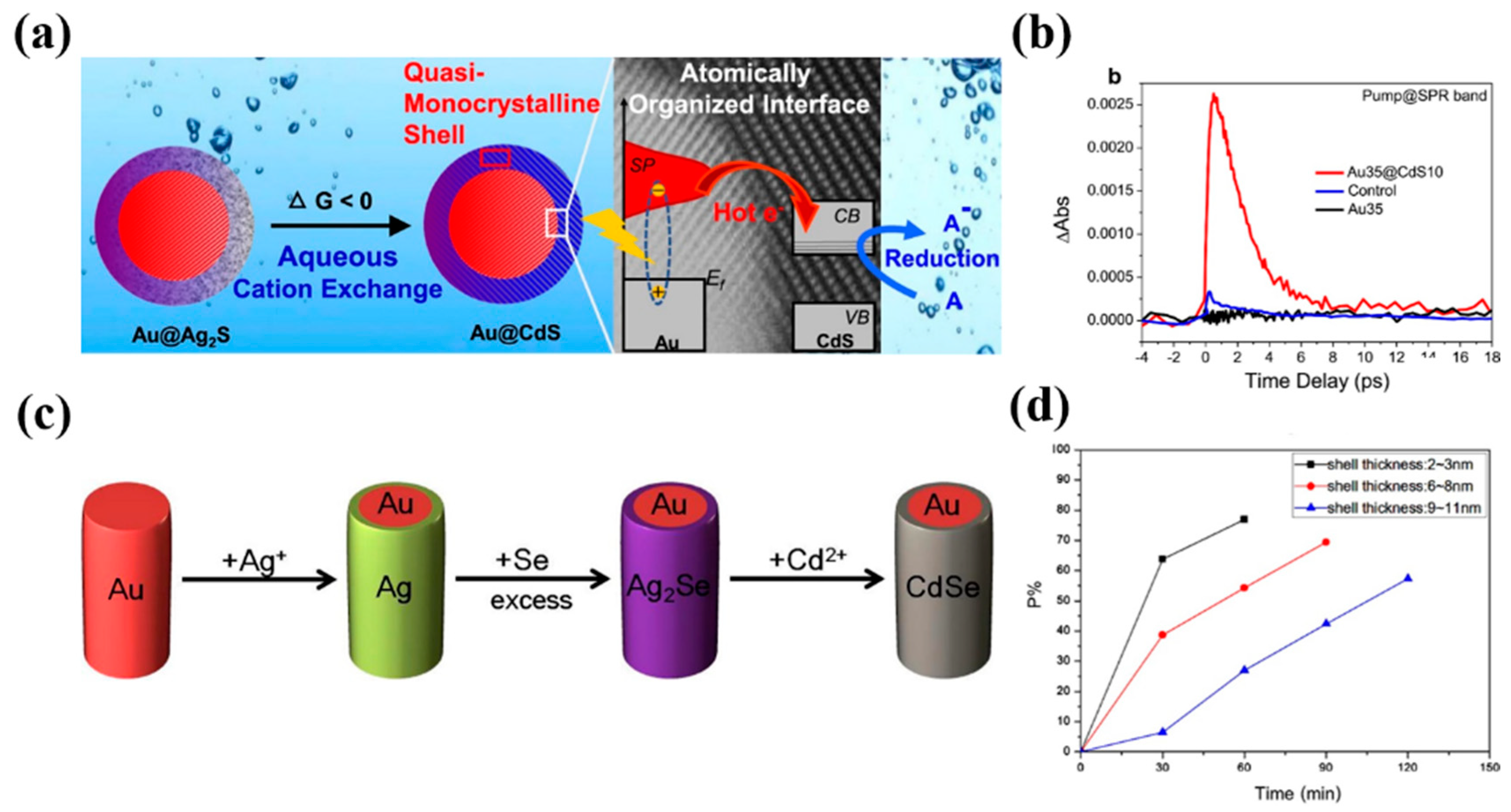
  92. Liu, J.; Feng, J.; Gui, J.; Chen, T.; Xu, M.; Wang, H.; Dong, H.; Chen, H.; Li, X.; Wang, L.; et al. Metal@semiconductor core-shell nanocrystals with atomically organized interfaces for efficient hot electron-mediated photocatalysis. Nano Energy 2018, 48, 44–52. [Google Scholar] [CrossRef]
  93. Lim, S.C.; Lo, W.F.; Yang, P.Y.; Lu, S.C.; Joplin, A.; Link, S.; Chang, W.S.; Tuan, H.Y. Au@CdSe heteroepitaxial nanorods: An example of metal nanorods fully covered by a semiconductor shell with strong photo-induced interfacial charge transfer effects. J. Colloid Interface Sci. 2018, 532, 143–152. [Google Scholar] [CrossRef] [PubMed]
  94. Liu, L.; Ouyang, S.; Ye, J. Gold-Nanorod-Photosensitized Titanium Dioxide with Wide-Range Visible-Light Harvesting Based on Localized Surface Plasmon Resonance. Angew. Chem. Int. Edit. 2013, 52, 6689–6693. [Google Scholar] [CrossRef]
  95. Leschkies, K.S.; Divakar, R.; Basu, J.; Enache-Pommer, E.; Boercker, J.E.; Carter, C.B.; Kortshagen, U.R.; Norris, D.J.; Aydil, E.S. Photosensitization of ZnO nanowires with CdSe quantum dots for photovoltaic devices. Nano Lett. 2007, 7, 1793–1798. [Google Scholar] [CrossRef]
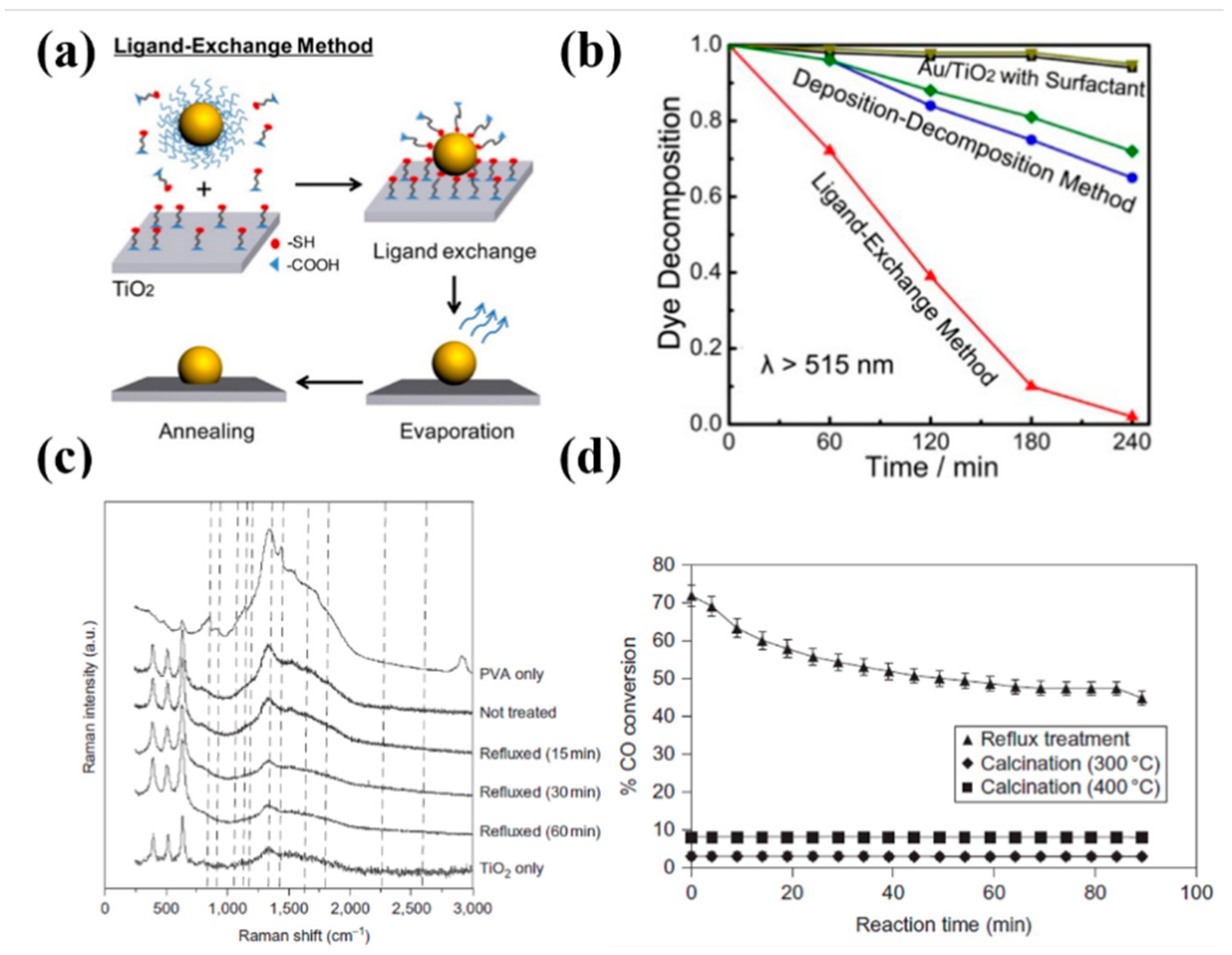
  96. Ding, D.; Liu, K.; He, S.; Gao, C.; Yin, Y. Ligand-exchange assisted formation of Au/TiO2 schottky contact for visible-light photocatalysis. Nano Lett. 2014, 14, 6731–6736. [Google Scholar] [CrossRef]
  97. Lopez-Sanchez, J.A.; Dimitratos, N.; Hammond, C.; Brett, G.L.; Kesavan, L.; White, S.; Miedziak, P.; Tiruvalam, R.; Jenkins, R.L.; Carley, A.F.; et al. Facile removal of stabilizer-ligands from supported gold nanoparticles. Nat. Chem. 2011, 3, 551–556. [Google Scholar] [CrossRef]
  98. Ge, Y.; Duan, X.; Zhang, M.; Mei, L.; Hu, J.; Hu, W.; Duan, X. Direct room temperature welding and chemical protection of silver nanowire thin films for high performance transparent conductors. J. Am. Chem. Soc. 2017, 140, 193–199. [Google Scholar] [CrossRef]
  99. Shan, F.; Zhang, X.Y.; Fu, X.C.; Zhang, L.J.; Su, D.; Wang, S.J.; Wu, J.Y.; Zhang, T. Investigation of simultaneously existed Raman scattering enhancement and inhibiting fluorescence using surface modified gold nanostars as SERS probes. Sci. Rep. 2017, 7, 6813. [Google Scholar] [CrossRef] [Green Version]
  100. Zhang, X.Y.; Xu, J.J.; Wu, J.Y.; Shan, F.; Ma, X.D.; Chen, Y.Z.; Zhang, T. Seeds triggered massive synthesis and multi-step room temperature post-processing of silver nanoink-application for paper electronics. RSC Adv. 2017, 7, 8–19. [Google Scholar] [CrossRef]
  101. Xu, Z.; Lin, Y.; Yin, M.; Zhang, H.; Cheng, C.; Lu, L.; Xue, X.; Fan, H.J.; Chen, X.; Li, D. Understanding the Enhancement Mechanisms of Surface Plasmon-Mediated Photoelectrochemical Electrodes: A Case Study on Au Nanoparticle Decorated TiO2 Nanotubes. Adv. Mater. Interfaces 2015, 2, 1500169. [Google Scholar] [CrossRef]
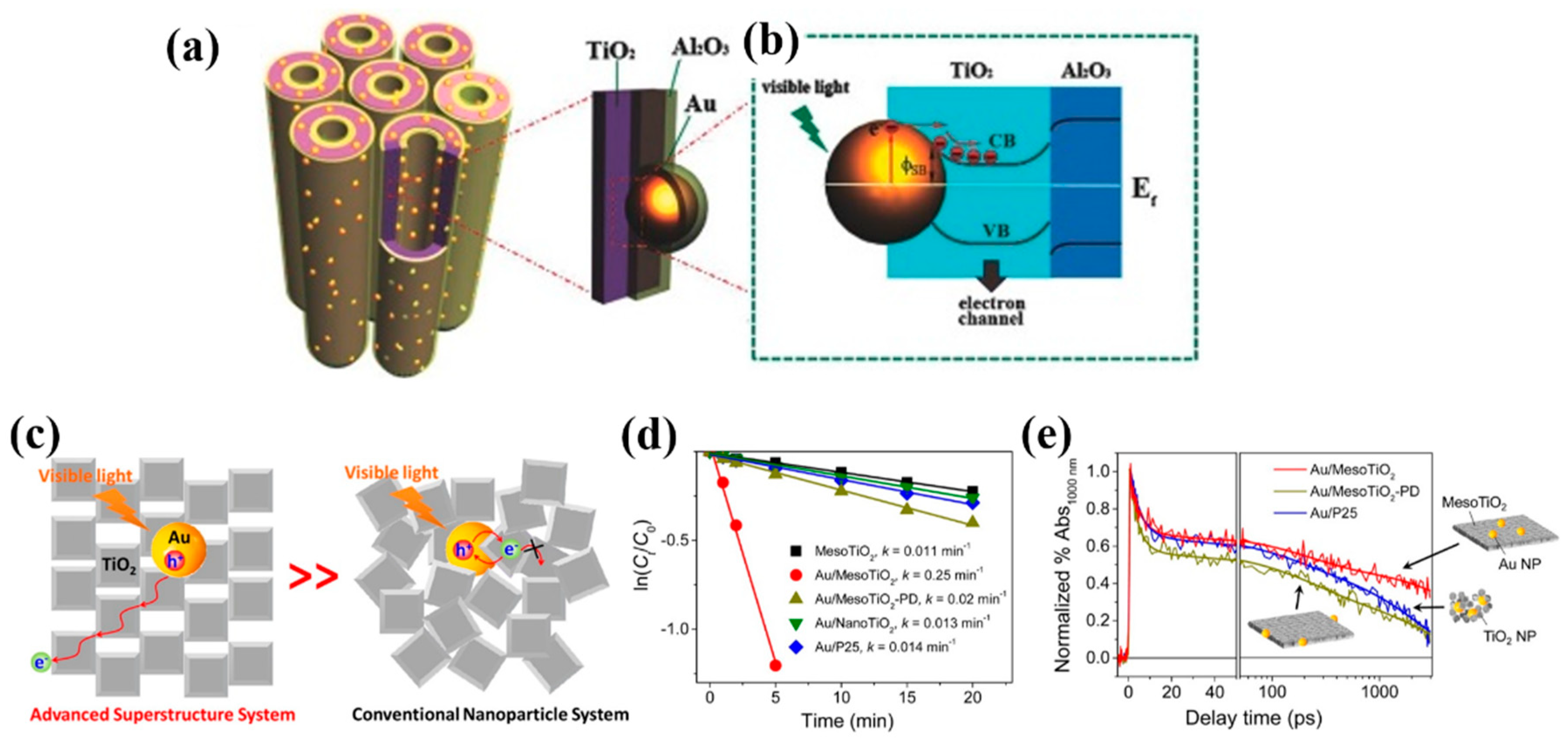
  102. Bian, Z.; Tachikawa, T.; Zhang, P.; Fujitsuka, M.; Majima, T. Au/TiO2 superstructure-based plasmonic photocatalysts exhibiting efficient charge separation and unprecedented activity. J. Am. Chem. Soc. 2013, 136, 458–465. [Google Scholar] [CrossRef]
  103. Hao, C.H.; Guo, X.N.; Sankar, M.; Yang, H.; Ma, B.; Zhang, Y.F.; Tong, X.L.; Jin, G.Q.; Guo, X.Y. Synergistic Effect of Segregated Pd and Au Nanoparticles on Semiconducting SiC for Efficient Photocatalytic Hydrogenation of Nitroarenes. ACS Appl. Mater. Interfaces 2018, 10, 23029–23036. [Google Scholar] [CrossRef]
  104. Li, X.; McNaughter, P.D.; O’Brien, P.; Minamimoto, H.; Murakoshi, K. Plasmonically enhanced electromotive force of narrow bandgap PbS QD-based photovoltaics. Phys. Chem. Chem. Phys. 2018, 20, 14818–14827. [Google Scholar] [CrossRef]
  105. Liu, G.; Wang, T.; Zhou, W.; Meng, X.; Zhang, H.; Liu, H.; Kako, T.; Ye, J. Crystal-facet-dependent hot-electron transfer in plasmonic-Au/semiconductor heterostructures for efficient solar photocatalysis. J. Mater. Chem. C 2015, 3, 7538–7542. [Google Scholar] [CrossRef] [Green Version]
  106. Bai, S.; Li, X.; Kong, Q.; Long, R.; Wang, C.; Jiang, J.; Xiong, Y. Toward enhanced photocatalytic oxygen evolution: Synergetic utilization of plasmonic effect and schottky junction via interfacing facet selection. Adv. Mater. 2015, 27, 3444–3452. [Google Scholar] [CrossRef]
  107. Zhou, C.; Wang, S.; Zhao, Z.; Shi, Z.; Yan, S.; Zou, Z. A Facet-Dependent Schottky-Junction Electron Shuttle in a BiVO4 {010}–Au–Cu2O Z-Scheme Photocatalyst for Efficient Charge Separation. Adv. Funct. Mater. 2018, 28, 1801214. [Google Scholar] [CrossRef]
  108. Li, Z.; Gao, Y.; Zhang, L.; Fang, Y.; Wang, P. Polarization-dependent surface plasmon-driven catalytic reaction on a single nanowire monitored by SERS. Nanoscale 2018, 10, 18720–18727. [Google Scholar] [CrossRef]
  109. Lee, C.; Lee, Y.K.; Park, Y.; Park, J.Y. Polarization Effect of Hot Electrons in Tandem-Structured Plasmonic Nanodiode. ACS Photonics 2018, 5, 3499–3506. [Google Scholar] [CrossRef]
  110. Gong, T.; Munday, J.N. Angle-independent hot carrier generation and collection using transparent conducting oxides. Nano Lett. 2014, 15, 147–152. [Google Scholar] [CrossRef]
  111. Li, W.; Coppens, Z.J.; Besteiro, L.V.; Wang, W.; Govorov, A.O.; Valentine, J. Circularly polarized light detection with hot electrons in chiral plasmonic metamaterials. Nat. Commun. 2015, 6, 8379. [Google Scholar] [CrossRef] [PubMed]
  112. Zhang, X.Y.; Zhou, H.L.; Shan, F.; Xue, X.M.; Su, D.; Liu, Y.R.; Chen, Y.Z.; Wu, J.Y.; Zhang, T. Synthesis of silver nanoplate based two-dimension plasmonic platform from 25 nm to 40 μm: Growth mechanism and optical characteristic investigation in situ. RSC Adv. 2017, 7, 55680–55690. [Google Scholar] [CrossRef]
  113. Gao, M.; Connor, P.K.N.; Ho, G.W. Plasmonic photothermic directed broadband sunlight harnessing for seawater catalysis and desalination. Energy Environ. Sci. 2016, 9, 3151–3160. [Google Scholar] [CrossRef] [Green Version]
  114. Liu, Y.; Lou, J.; Ni, M.; Song, C.; Wu, J.; Dasgupta, N.P.; Tao, P.; Shang, W.; Deng, T. Bioinspired bifunctional membrane for efficient clean water generation. ACS Appl. Mater. Interfaces 2015, 8, 772–779. [Google Scholar] [CrossRef] [PubMed]
  115. Zhang, X.Y.; Shan, F.; Zhou, H.L.; Su, D.; Xue, X.M.; Wu, J.Y.; Chen, Y.Z.; Zhao, N.; Zhang, T. Silver nanoplate aggregation based multifunctional black metal absorbers for localization, photothermic harnessing enhancement and omnidirectional light antireflection. J. Mater. Chem. C 2018, 6, 989–999. [Google Scholar] [CrossRef]
  116. Souzandeh, H.; Johnson, K.S.; Wang, Y.; Bhamidipaty, K.; Zhong, W.H. Soy-protein-based nanofabrics for highly efficient and multifunctional air filtration. ACS Appl. Mater. Interfaces 2016, 8, 20023–20031. [Google Scholar] [CrossRef]
  117. Xiong, Z.C.; Yang, R.L.; Zhu, Y.J.; Chen, F.F.; Dong, L.Y. Flexible hydroxyapatite ultralong nanowire-based paper for highly efficient and multifunctional air filtration. J. Mater. Chem. A 2017, 5, 17482–17491. [Google Scholar] [CrossRef]
  118. Lv, D.; Wang, R.; Tang, G.; Mou, Z.; Lei, J.; Han, J.; Smedt, S.D.; Xiong, R.; Huang, C. Eco-friendly Electrospun Membranes Loaded with Visible-light Response Nano-particles for Multifunctional usages: High-efficient Air Filtration, Dye Scavenger and Bactericide. ACS Appl. Mater. Interfaces 2019, 11, 12880–12889. [Google Scholar] [CrossRef] [PubMed]
  119. Jeong, S.; Cho, H.; Han, S.; Won, P.; Lee, H.; Hong, S.; Yeo, J.; Kwon, J.; Ko, S.H. High efficiency, transparent, reusable, and active PM2. 5 filters by hierarchical Ag nanowire percolation network. Nano Lett. 2017, 17, 4339–4346. [Google Scholar] [CrossRef]
  120. Zhang, X.Y.; Xue, X.M.; Zhou, H.L.; Zhao, N.; Shan, F.; Su, D.; Liu, Y.R.; Zhang, T. Seeds screening aqueous synthesis, multiphase interfacial separation and in situ optical characterization of invisible ultrathin silver nanowires. Nanoscale 2018, 10, 15468–15484. [Google Scholar] [CrossRef] [PubMed]
  121. Björklund, K.; Li, L. Evaluation of low-cost materials for sorption of hydrophobic organic pollutants in stormwater. J. Environ. Manag. 2015, 159, 106–114. [Google Scholar] [CrossRef] [PubMed]
  122. Liu, C.; Hsu, P.C.; Lee, H.W.; Ye, M.; Zheng, G.; Liu, N.; Li, W.; Cui, Y. Transparent air filter for high-efficiency PM2.5 capture. Nat. Commun. 2015, 6, 6205–6214. [Google Scholar] [CrossRef] [PubMed]
  123. Xu, J.; Liu, C.; Hsu, P.C.; Liu, K.; Zhang, R.; Liu, Y.; Cui, Y. Roll-to-Roll Transfer of Electrospun Nanofiber Film for High-Efficiency Transparent Air Filter. Nano Lett. 2016, 16, 1270–1275. [Google Scholar] [CrossRef] [PubMed]
  124. Zhao, Y.; Low, Z.X.; Feng, S.; Zhong, Z.; Wang, Y.; Yao, Z. Multifunctional hybrid porous filters with hierarchical structures for simultaneous removal of indoor VOCs, dusts and microorganisms. Nanoscale 2017, 9, 5433–5444. [Google Scholar] [CrossRef] [PubMed]
  125. Wu, J.; Huang, Y.; Ye, W.; Li, Y. CO2 reduction: From the electrochemical to photochemical approach. Adv. Sci. 2017, 4, 1700194. [Google Scholar] [CrossRef]
  126. Low, J.; Cheng, B.; Yu, J. Surface modification and enhanced photocatalytic CO2 reduction performance of TiO2: A review. Appl. Surf. Sci. 2017, 392, 658–686. [Google Scholar] [CrossRef]
  127. Chang, X.; Wang, T.; Gong, J. CO2 photo-reduction: Insights into CO2 activation and reaction on surfaces of photocatalysts. Energy Environ. Sci. 2016, 9, 2177–2196. [Google Scholar] [CrossRef]
  128. Zhang, L.; Zhao, Z.J.; Gong, J. Nanostructured materials for heterogeneous electrocatalytic CO2 reduction and their related reaction mechanisms. Angew. Chem. Int. Edit. 2017, 56, 11326–11353. [Google Scholar] [CrossRef]
  129. Lang, X.; Chen, X.; Zhao, J. Heterogeneous visible light photocatalysis for selective organic transformations. Chem. Soc. Rev. 2014, 43, 473–486. [Google Scholar] [CrossRef]
  130. Corrigan, N.; Shanmugam, S.; Xu, J.; Boyer, C. Photocatalysis in organic and polymer synthesis. Chem. Soc. Rev. 2016, 45, 6165–6212. [Google Scholar] [CrossRef]
  131. Li, B.; Zhang, B.; Nie, S.; Shao, L.; Hu, L. Optimization of plasmon-induced photocatalysis in electrospun Au/CeO2 hybrid nanofibers for selective oxidation of benzyl alcohol. J. Catal. 2017, 348, 256–264. [Google Scholar] [CrossRef]
  132. Han, D.; Bao, Z.; Xing, H.; Yang, Y.; Ren, Q.; Zhang, Z. Fabrication of plasmonic Au–Pd alloy nanoparticles for photocatalytic Suzuki–Miyaura reactions under ambient conditions. Nanoscale 2017, 9, 6026–6032. [Google Scholar] [CrossRef]
  133. Yurdakal, S.; Tek, B.S.; Değirmenci, Ç.; Palmisano, G. Selective photocatalytic oxidation of aromatic alcohols in solar-irradiated aqueous suspensions of Pt, Au, Pd and Ag loaded TiO2 catalysts. Catal. Today 2017, 281, 53–59. [Google Scholar] [CrossRef]
  134. Zhao, J.; Nguyen, S.C.; Ye, R.; Ye, B.; Weller, H.; Somorjai, G.A.; Alivisatos, A.P.; Toste, F.D. A comparison of photocatalytic activities of gold nanoparticles following plasmonic and interband excitation and a strategy for harnessing interband hot carriers for solution phase photocatalysis. ACS Cent. Sci. 2017, 3, 482–488. [Google Scholar] [CrossRef] [PubMed]
  135. Minutella, E.; Schulz, F.; Lange, H. Excitation-dependence of plasmon-induced hot electrons in gold nanoparticles. J. Phys. Chem. Lett. 2017, 8, 4925–4929. [Google Scholar] [CrossRef] [PubMed]
  136. Zhou, L.; Swearer, D.F.; Zhang, C.; Robatjazi, H.; Zhao, H.; Henderson, L.; Dong, L.; Christopher, P.; Carter, E.A.; Nordlander, P.; et al. Quantifying hot carrier and thermal contributions in plasmonic photocatalysis. Science 2018, 362, 69–72. [Google Scholar] [CrossRef] [Green Version]
  137. Meng, X.; Liu, L.; Ouyang, S.; Xu, H.; Wang, D.; Zhao, N.; Ye, J. Nanometals for Solar-to-Chemical Energy Conversion: From Semiconductor-Based Photocatalysis to Plasmon-Mediated Photocatalysis and Photo-Thermocatalysis. Adv. Mater. 2016, 28, 6781–6803. [Google Scholar] [CrossRef] [PubMed]
  138. Zhang, X.; Li, X.; Reish, M.E.; Zhang, D.; Su, N.Q.; Gutiérrez, Y.; Moreno, F.; Yang, W.; Everitt, H.O.; Liu, J. Plasmon-enhanced catalysis: Distinguishing thermal and nonthermal effects. Nano Lett. 2018, 18, 1714–1723. [Google Scholar] [CrossRef]
  139. Swearer, D.F.; Leary, R.K.; Newell, R.; Yazdi, S.; Robatjazi, H.; Zhang, Y.; Renard, D.; Nordlander, P.; Midgley, P.A.; Halas, N.J.; et al. Transition-metal decorated aluminum nanocrystals. ACS Nano 2017, 11, 10281–10288. [Google Scholar] [CrossRef]
  140. Shaik, F.; Peer, I.; Jain, P.K.; Amirav, L. Plasmon-Enhanced Multicarrier Photocatalysis. Nano Lett. 2018, 18, 4370–4376. [Google Scholar] [CrossRef]
  141. Wang, R.; Purdie, D.G.; Fan, Y.; Massabuau, F.C.-P.; Braeuninger-Weimer, P.; Burton, O.J.; Blume, R.; Schloegl, R.; Lombardo, A.; Weatherup, R.S.; et al. A Peeling Approach for Integrated Manufacturing of Large Monolayer h-BN Crystals. ACS Nano 2019, 13, 2114–2126. [Google Scholar] [CrossRef] [PubMed] [Green Version]
  142. Bhandari, S.; Hao, B.; Waters, K.; Lee, C.H.; Idrobo, J.C.; Zhang, D.; Pandey, R.; Yap, Y.K. Two-Dimensional Gold Quantum Dots with Tunable Bandgaps. ACS Nano 2019, 13, 4347–4353. [Google Scholar] [CrossRef]
  143. Tom, K.B.; Lin, S.; Wan, L.F.; Wang, J.; Ahlm, N.; N’Diaye, A.T.; Bustillo, K.; Huang, J.; Liu, Y.; Lou, S.; et al. Solution-Based, Template-Assisted Realization of Large-Scale Graphitic ZnO. ACS Nano 2018, 12, 7554–7561. [Google Scholar] [CrossRef]
  144. Jang, Y.J.; Chung, K.; Lee, J.S.; Choi, C.H.; Lim, J.W.; Kim, D.H. Plasmonic Hot Carriers Imaging: Promise and Outlook. ACS Photonics 2018, 5, 4711–4723. [Google Scholar] [CrossRef]
  145. Keller, E.L.; Frontiera, R.R. Ultrafast nanoscale Raman thermometry proves heating is not a primary mechanism for plasmon-driven photocatalysis. ACS Nano 2018, 12, 5848–5855. [Google Scholar] [CrossRef] [PubMed]
  146. Lou, Z.; Kim, S.; Zhang, P.; Shi, X.; Fujitsuka, M.; Majima, T. In situ observation of single Au triangular nanoprism etching to various shapes for plasmonic photocatalytic hydrogen generation. ACS Nano 2016, 11, 968–974. [Google Scholar] [CrossRef]
Figure 1. Process of the formation of the Schottky contact. (a) The band diagram before coming into contact with the metal and n-type semiconductor. (b) The flow of electrons from the n-type semiconductor to the metal and (c) the final equilibrium attainment with the bending of the band after contact.
Applsci 09 02093 g001
Figure 2. (a) The decay of excited surface plasmons (SPs) in plasmonic metal. (b) The transitions of hot carriers (HCs) in two ways, Intraband transition and Interband transition. (c) The scheme of transportation of HCs in plasmon induced hot-electron transfer (PHET) and (d) in plasmon induced metal-to-semiconductor interfacial charge transfer transition (PICTT). (e) The diffusions of HCs and the photocatalytic process of the redox reaction in plasmon-mediated heterostructure (PMH).
Applsci 09 02093 g002
Figure 3. “Tip hot spots” effects in plasmon-mediated heterostructures. (a) Calculated distributions of electromagnetic (EM) fields in nanospheres, nanorods and nanostars (from left to right). (b) Theoretical EM field enhancement factor in three typical metals. In the Au nanorod, the blue dot and red dot correspond to the EM field paralleled and perpendicular to the nanorods, respectively. In the Au nanostar, the different spike lengths, combined with a core of 25 nm, were calculated. (c) The theory and experiment results for the rates of the HCs’ generation in SiO2 loaded Au@TiO2. (ac) Reproduced with permission. [63] Copyright 2016, American Chemical Society. (d) The morphology of the Au nanorods@TiO2 dumbbells presented by transmission electron microscope (TEM). (e) The comparison of the rates of degradation of methyl blue (MB) in different Au rods/TiO2 heterostructures. (d,e) Reproduced with permission. [64] Copyright 2016, American Chemical Society. (f) The scheme of Au nanocubes@Cu2O heterostructures. (g) The amounts of H2 generation in four kinds of Au/Cu2O heterostructures. (f,g) Reproduced with permission. [65] Copyright 2016, American Chemical Society.
Applsci 09 02093 g003
Figure 4. “Gap hot spots” designed for an efficient photocatalytic process. (a) Calculated optical absorption cross section in a single Au sphere and Au nanodimers with different gap spaces. (b) The theoretical relationships between the rates of generation of HCs and the gap space. (a,b) Reproduced with permission. [69] Copyright 2016, American Chemical Society. (c) The scheme of “hot spots” structures built up by Au rods-TiO2/thermoresponsive polymer and (d) the rates of degradation of RhB under 25 °C (blue regions) and 40 °C (red regions). (c,d) Reproduced with permission. [70] Copyright 2018, Wiley-VCH. (e) The absorption spectrum of Au@MOS2 with different numbers of the Au core and (f) the corresponding distributions of the EM fields under a certain incident light (630 nm). Finally, (g) the rates of H2 generation in these structures. (eg) Reproduced with permission. [71] Copyright 2016, Elsevier Ltd.
Applsci 09 02093 g004
Figure 5. The design of the plasmonic cavity for broad band photons trapping. (a) The schematic of Au NPs-TiO2 layers-Au films “sandwich structures” (the inset is the transportation of incident photons between Au NPs and Au films). (b) The comparison of the absorption spectrum in absorbers-spacer-mirror (ASM) structures with control groups. (a,b) Reproduced with permission. [74] Copyright 2016, American Chemical Society. (c) The band diagram and flow of HCs in Au nanorods-TiO2 dumbbells/Au films under visible light illumination. (d) The comparison of rates of decomposing MB in Au/TiO2/ITO and Au/TiO2/ITO under different wavelengths of the incident light, respectively. (c,d) Reproduced with permission. [75] Copyright 2018, Wiley-VCH. (e) The scheme of surface plasmon polaritons (SPPs)-mediated broadband light absorption structures, which was built up by pattered Ag gratings, TiO2 layers and Al films (from top to bottom). (f) The total absorption of rectangular gratings (RG) and trapezoidal gratings (TGs) on top, respectively. (e,f) Reproduced with permission. [78] Copyright 2018, Springer.
Applsci 09 02093 g005
Figure 6. The scheme of the pathway of light in (a) 3D-array Au-TiO2 hollow structures and random distributions of Au-TiO2 under visible light illumination (>420 nm), and (b) in single Au-TiO2 hollow and TiO2 hollow structures under simulated daylight. The comparison of the amounts of H2 production in three typical structures under (c) simulated daylight and (d) visible light illumination (>420 nm). Reproduced with permission. [82] Copyright 2016, American Chemical Society.
Applsci 09 02093 g006
Figure 7. The synthesis of high quality heterostructures. (a) The scheme of the method of aqueous cation exchange for Au@CdS heterostructures and (b) the transient absorption spectrum of three types of structures, Au35@CdS10 (the sizes of the Au core and CdS shell are 35 nm and 10 nm, respectively.), Control (Au35@CdS10 prepared by conventional methods) and Au35 (pure Au sphere with a diameter of 35 nm), pumped at the center surface plasmon resonance (SPR) band. (a,b) Reproduced with permission. [92] Copyright 2018, Elsevier Ltd. (c) The scheme in the synthesis of cylindrical Au@ CdSe heterostructures and (d) the rates of degradation of MB with different thicknesses of the CdSe shell. (c,d) Reproduced with permission. [93] Copyright 2018, Elsevier Ltd.
Applsci 09 02093 g007
Figure 8. The efficient transfer of HCs by involving a post-treatment. (a) The scheme for forming a compact contact between Au and TiO2 by ligand exchange and annealing, successively. (b) The rates of dye decomposition under different methods. (a,b) Reproduced with permission. [96] Copyright 2014, American Chemical Society. (c) The measured Raman intensity of Au/TiO2 under different refluxed times. (d) The conversing efficiency of CO in Au/TiO2 treated by reflux treatment and high-temperature calcination (300 °C and 400 °C). (c,d) Reproduced with permission. [97] Copyright 2011, Springer Nature.
Applsci 09 02093 g008
Figure 9. The methods to separate charges transported to the interface. (a) The scheme of TiO2 nanotube-Al2O3-Au and (b) the process of transfer of HCs under visible light illumination. (a,b) Reproduced with permission. [101] Copyright 2015, Wiley-VCH. (c) The scheme of the flowing of HCs in ordered Au-TiO2 structures and that in random structures. (d) The rates of degradation of MB and (e) the life of HCs observed at 1000 nm in different Au/TiO2 systems. (ce) Reproduced with permission. [102] Copyright 2014, American Chemical Society.
Applsci 09 02093 g009
Figure 10. The design for the specific contact of the crystal face between the plasmonic metals and the semiconductor. (a) The scheme of the bending degree of the band structures and (b) the measurement of the current density in BiOCl-001-Au and BiOCl-010-Au. (a,b) Reproduced with permission. [105] Copyright 2015, The Royal Society of Chemistry. (c) The scheme of the band structures and (d) the structural design in Ag-(001)BiOCl(110)-Pd hybrid structures. (e) The rates of the photocatalytic oxygen production in BiOCL, BiOCl (110)-Pd, Ag-(001) BiOCl and Ag-(001)BiOCl(110)-Pd. (ce) Reproduced with permission. [106] Copyright 2015, Wiley-VCH.
Applsci 09 02093 g010
Figure 11. The effect of the polarization of light on metal-semiconductor heterostructures. (a) The scheme of light excited on a single Ag nanowire under a microscope. (b) The Raman intensity of 4NBT and (c) the contents of the converted DMAB under different angles of the incident light. (ac) Reproduced with permission. [108] Copyright 2018, the Royal Society of Chemistry. (d) The scheme of the tunable polarization of light and (e) the transportation of HCs under both longitudinal and transverse modes. (f) The response of the photocurrent in the thin film Au/TiO2, 2D Au/TiO2 and 3D tandem Au/TiO2 by rotating the angles from 0 to 360 °C. (df) Reproduced with permission. [109] Copyright 2018, American Chemical Society.
Applsci 09 02093 g011
Figure 12. Membrane based PMH photocatalysts for water/air purifications. (a) The scheme of the fabrication of a bifunctional membrane and (b) the synergistic effects in the steam generation and pollutants decomposition. (c) The rates of degradation of RhB in Au-AAO, TiO2-AAO and TiO2-Au-AAO. (ac) Reproduced with permission. [114] Copyright 2016, American Chemical Society. (d) The scheme for designing Ag@CNTs/Al2O3 filters by chemical vapor deposition and a polyol process. (e) The antimicrobic rates and (f) degradation rates of volatile organic compounds (VOCs) in different purification filters. (df) Reproduced with permission. [124] Copyright 2017, the Royal Society of Chemistry.
Applsci 09 02093 g012

