Article

3D Printed High Gain Complementary Dipole/Slot Antenna Array

1
State Key Laboratory of Millimeter Waves, City University of Hong Kong, Kowloon, Hong Kong
2
State Key Laboratory of Millimeter Waves, Department of Electronic Engineering, City University of Hong Kong, Kowloon, Hong Kong
*
Author to whom correspondence should be addressed.
Appl. Sci. 2018, 8(8), 1410; https://doi.org/10.3390/app8081410
Submission received: 31 July 2018 / Revised: 13 August 2018 / Accepted: 15 August 2018 / Published: 20 August 2018
(This article belongs to the Special Issue 3D Printed Antennas)

Abstract

:

Featured Application

This paper introduces an in-house fabrication of a high gain complementary dipole/slot antenna array at the Ka-band using 3D printing technology followed by metallization via electroplating. The proposed antenna array features a comparable performance to commercial counterparts, with a lower cost and lighter weight. This antenna array has potential use for fifth generation wireless communication applications.

Abstract

By employing the complementary dipole antenna concept to the normal waveguide fed slot radiator, an improved antenna element with wide impedance bandwidth and symmetrical radiation patterns is developed. This is achieved by mounting two additional metallic cuboids on the top of the slot radiator, which is equivalent to adding an electric dipole on top of the magnetic dipole due to the slot radiator. Then, a high-gain antenna array was designed based on the improved element and fabricated, using 3D printing technology, with stable frequency characteristics operated at around 28 GHz. This was followed by metallization via electroplating. Analytical results agree well with the experimental results. The measured operating frequency range for the reflection coefficient ≤−15 dB is from 25.7 GHz to 29.8 GHz; its corresponding fractional impedance bandwidth is 14.8%. The measured gain is approximately 32 dBi, with the 3 dB beamwidth around 4°.

1. Introduction

Fifth generation (5G) wireless communications standard in the US was announced in July, 2016 by the Federal Communications Commission (FCC), which would provide a higher data rate than today’s Fourth Generation (4G) wireless networks. A particular spectrum that is in the higher bands for the new Upper Microwave Flexible Use Service is in 28 GHz (from 27.5 GHz to 28.35 GHz). This millimeter-wave band for 5G cellular network was demonstrated by Rappaport and his research team as early as in 2013 [1].
To ensure a sufficient link budget at millimeter-wave band, high gain antennas are required. The waveguide slot antenna is normally used as the basic element to realize a high gain antenna array. The slot element possesses advantages of low cross polarization, high radiation efficiency and planar features, whereas it mainly suffers from the drawback of a narrow impedance bandwidth. Applications for using slot-waveguides for optical devices, such as demultiplexers and power splitters, have been proposed [2,3,4]. These are more convenient for combining the device to the antenna input. The fractional impedance bandwidth of most slot antenna arrays is in the order of a few percent. Some improved designs have achieved more than 10% [5,6,7,8]. In Reference [9], a planar waveguide slot antenna array in the Ku-band was developed with 256 slot elements, where the basic radiating unit is a cavity-backed 2 × 4 slot subarray. Therefore, 32 subarrays were grouped together and connected by an equal amplitude and equal phase parallel waveguide feed network. Through the use of the 2 × 4 slot subarray, the design of the feeding circuitry was simplified significantly, as the subarray with 8 slot radiators were concurrently excited by a common backing cavity. This design is also helpful for achieving higher aperture efficiency as the single subarray showed an 18 dBi gain performance, much higher than that of a single slot element. The measured efficiency of the array was around 85% which is higher than the printed microstrip array technique [10,11]. In addition, the measured impedance bandwidth was 12% (Standing Wave Ratio (SWR) <2), which is relatively wide for the waveguide slot antenna. For the 5G waveguide slot antenna array operating from 40.5 GHz to 43.5 GHz [6], it has 24 × 24 elements with a 33.8 dBi maximum gain, and a gain variation of 2.1 dB. The obtained impedance bandwidth was 5.5% (SWR <2), where each subarray consisted of 6 × 6 radiating slots. Another design by Ando and his research team was demonstrated at 60 GHz with a 32 dBi gain over a 4.8 GHz bandwidth [12]. A full-corporate-feed network was integrated to the antenna array to achieve wideband performance, in comparison to the series-feed design. The measured fractional impedance bandwidth is 8.3% for reflection coefficient <−14 dB, which is acceptable at such a high frequency band. A wide slot radiator was used as the basic radiating unit with an aspect ratio of 0.64.
By applying the concept of the complementary antenna [13,14,15,16,17,18,19] for each radiating element, an electric dipole, consisting of two metallic cuboids, was introduced to each slot of the waveguide slot array in Reference [20] for Ku-band applications. The whole structure was constructed using aluminum. The element can be considered a simplified version of the Clavin element [13]. In this paper, the complementary dipole antenna array is enhanced for 28-GHz applications and ease of fabrication using 3D printing and electroplating. Metallization of 3D printed W-band bandpass filters has been demonstrated in Reference [21]. The metallization process consisted of electroless plating followed by electroplating. In this paper, the electroless plating is replaced by simple coating of a thin copper film on the 3D printed surface using a spraying gun. This process has the advantages of low cost, light weight, and stable gain within the operating band. Measurements were undertaken to verify the simulations and the measured results agree well with the simulated ones.

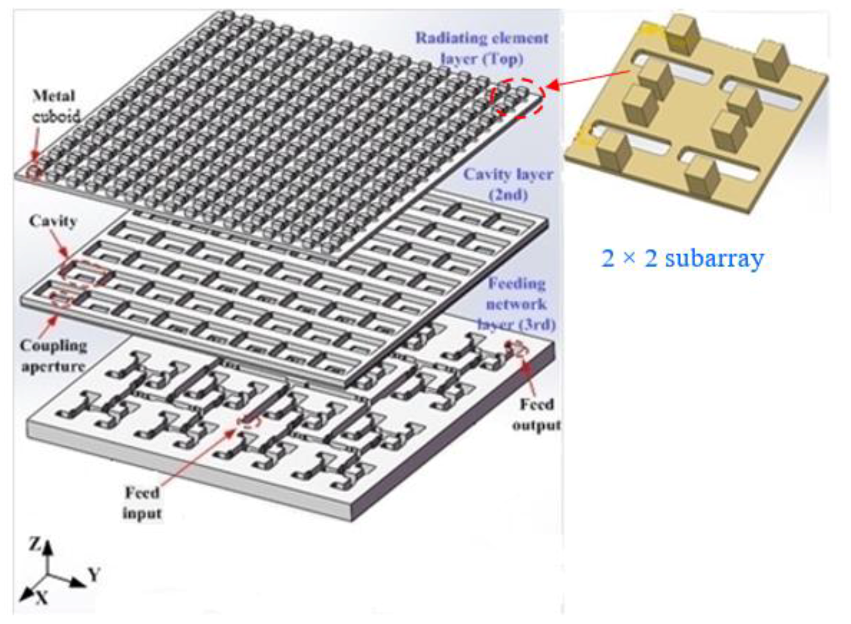
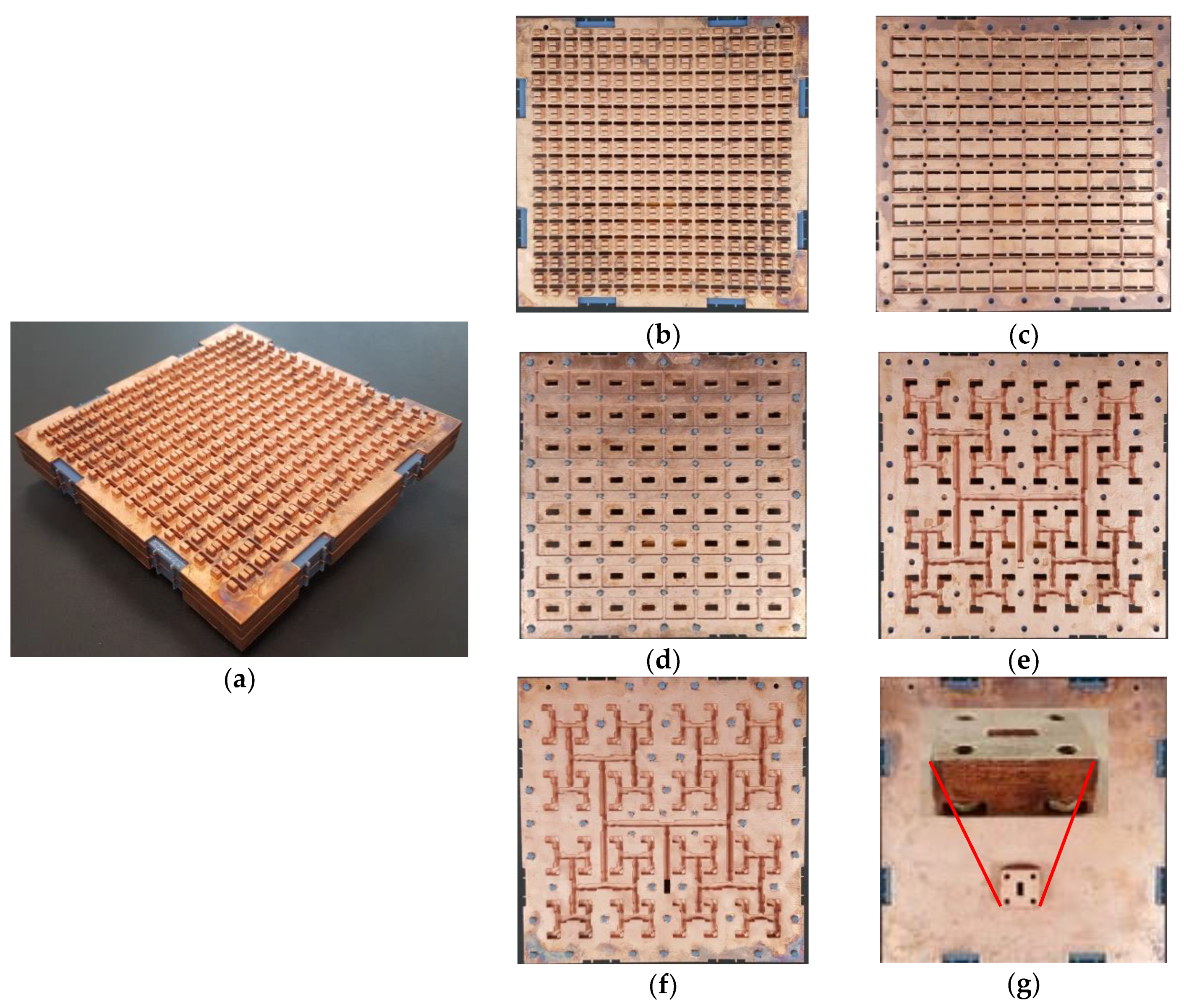
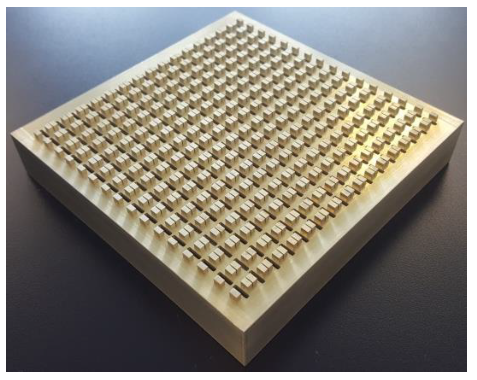
2. Design and Fabrication of a 16 × 16 Complementary Dipole Antenna Array

Figure 1 shows an expanded perspective view of the proposed 16 × 16 complementary dipole antenna array (139.5 mm × 139.3 mm × 16.2 mm). To reduce the fabrication tolerance, the antenna array should minimize the number of layers to prevent the structure deteriorating. The cutting layer was determined using the weakness current at the surface of the structure using simulation software. It was then determined whether or not the top and bottom of the cutting layer can be easily sprayed. The final array was composed of three layers. The bottom layer is the feeding network, which is constructed using 90° waveguide H-bends to transfer energy from the bottom WR-28 (7.112 mm × 3.556 mm) waveguide input layer. E-type waveguide T-junction splitters are used to divide the incoming signal with equal amplitude and 180° phase difference. Such a power-dividing operation is conducted in six stages. The impedance matching stubs not only provide the impedance matching capability, but also the polarization rotation effect of the E-field inside the waveguide structures. The final E-field polarizations at all of the output ports of the impedance matching stubs are focused in the same direction. The middle layer has the 64 rectangular cavities (14.85 mm × 10.35 mm × 2.7 mm) with coupling apertures (6.075 mm × 2.25 mm) which force the 64 sets of the 2 × 2 subarray to radiate unidirectional broadside patterns. The top layer has the 64 sets of the 2 × 2 subarray, containing 256 slots (6.3 mm × 0.9 mm × 1.8 mm) and 512 metallic cuboids (3.6 mm × 2.25 mm × 2.7 mm). The four slots and eight cuboids form one 2 × 2 subarray. Each metallic cuboid with length = 0.21λ and the two cuboids’ separation width = 0.29λ work as an electric dipole, whereas the slot with length = 0.5λ is equivalent to a magnetic dipole. Combining these two radiators together, complementary dipole antenna element is obtained. The 16 × 16 complementary dipole antenna array was simulated using ANSYS High Frequency Structure Simulator (HFSS) 18.0.
To verify the simulation results, a prototype of the 16 × 16 complementary dipole antenna array was fabricated by 3D printing each layer using a Stratasys Objet30 Scholar system with VeroBlue RGD240 printing material. Its permittivity, ε r and loss tangent, tanδ were 2.9 and 0.01, respectively. The first layer had 256 slots, 512 metallic cuboids, and the upper half of 64 rectangular cavities. The second layer had the lower half of 64 rectangular cavities, 64 coupling apertures, and the upper half of the feeding network. Finally, the third layer had the lower half of the feeding network and the waveguide input port. After first spraying the 3D printed components with copper conductive paint, then electroplating with copper using a current of 1.8 A for an hour, the metallized structure was assembled by combining the three layers as shown in Figure 2. For seamless assembly of the array, cylindrical pegs (Figure 2d,f) and holes (Figure 2c,e) were printed at the top surface of Layers two and three and the bottom surface of Layers one and two, respectively. Four rectangular holes (6.54 mm × 5.6 mm × 2.5 mm) were used for the assembly of the four metallic nuts inside the waveguide flange as shown in Figure 2g. For comparison, an aluminum version of the 16 × 16 complementary dipole antenna array was also fabricated and is displayed in Figure 3. This was also fabricated by milling three aluminum layers followed by electroplating with copper. The three layers were soldered together to form the array. The 3D printed, and aluminum antenna arrays, weighed 0.35 kg and 1.36 kg, respectively. The antenna performance of the two arrays is demonstrated in the following section.

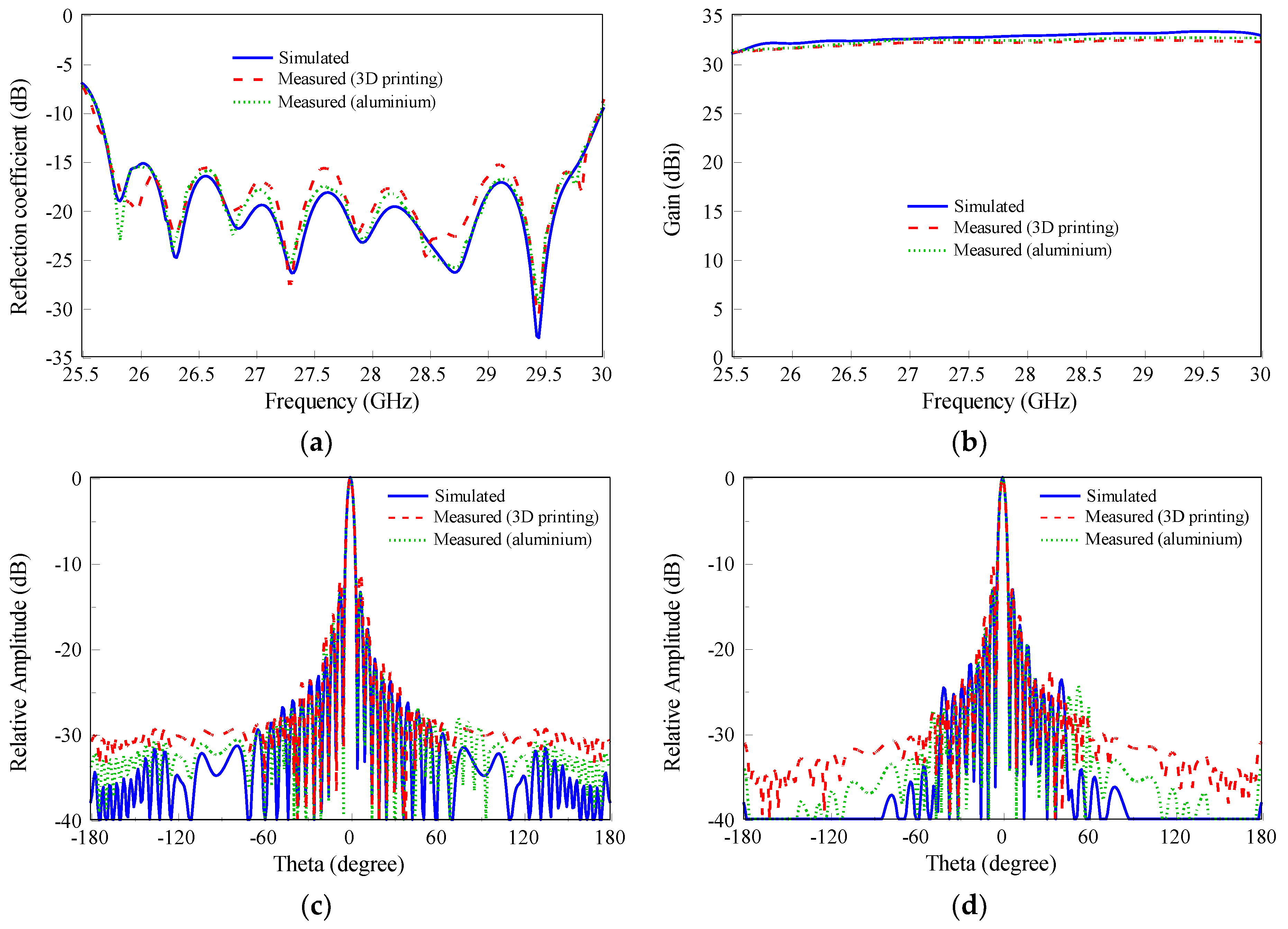
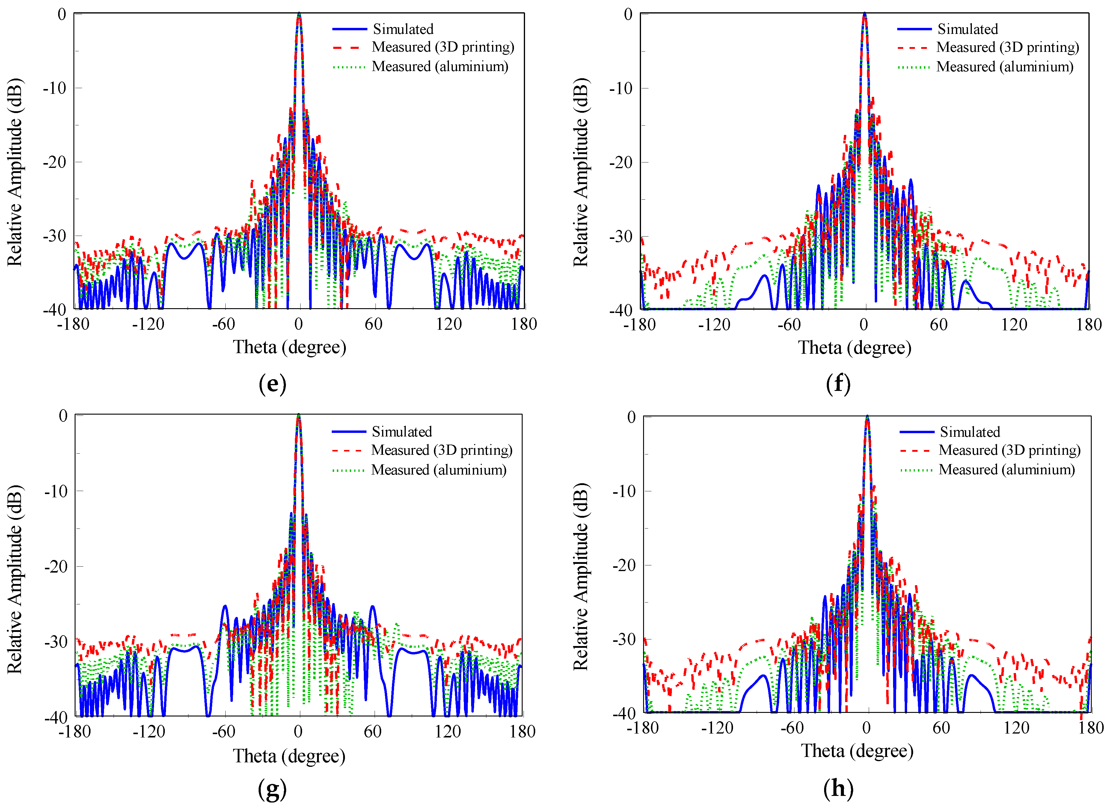
3. Measured and Simulated Results

To measure both the 3D printed and aluminum version of the 16 × 16 complementary dipole antenna arrays, the rectangular waveguide input port at the bottom layer was connected to a Millitech Inc. WCA-28-QSF00A waveguide-to-SubMiniature version A (SMA) adaptor. The reflection coefficient was measured using an Agilent Technologies E8363C network analyzer. Figure 4a shows the measured and simulated reflection coefficients of the 3D printed and aluminum arrays. For reflection coefficient ≤−15 dB, the measured impedance bandwidths of the 3D printed and aluminum arrays are 14.8% from 25.74 GHz to 29.85 GHz and 14.7% from 25.74 GHz to 29.81 GHz, respectively. In contrast, the simulated impedance bandwidth is 14.6% from 25.74 GHz to 29.80 GHz. The lower operating frequency in all three cases is 25.74 GHz and the maximum error in the upper operating frequency is only 0.17%.
The gain and radiation patterns are measured with a near-field antenna measurement system by Nearfield Systems Inc., (NSI). The measured gains for the 3D printed and aluminum arrays and the simulated gains are illustrated in Figure 4b. A high and stable gain of more than 31 dBi across the operating band is obtained for both the measurements and the simulation. The measured gain of the 3D printed version is only 0.4 dB lower than that of the aluminum version.
Figure 4c–h shows the measured radiation patterns of the 3D printed and aluminum arrays, as well as the simulated patterns at 25.74, 27.80, and 29.85 GHz, where the complementary dipole antenna array operates in a broadside symmetrical radiation in the phi = 0° and 90° planes. The measured first sidelobe levels of the 3D printed and aluminum arrays at 27.80 GHz are 13 dB at 0° and 90° planes. They are similar to the simulated levels at 27.80 GHz of 13.8 dB at 0° and 90° planes. The measured 3 dB beamwidths of the 3D printed and aluminum arrays in the 0° and 90° planes are 4.2° and 4° at 27.80 GHz, respectively. This is because the position of the dipole and the slot are placed at an orthogonal orientation and the electric dipole and magnetic dipoles are produced. From the above performances of the proposed antenna array, it demonstrates excellent radiation characteristics, including wideband, high gain, low back radiation, low cross-polarization levels, high front-to-back ratio, and symmetrical radiation patterns in the phi = 0° and 90° planes.

4. Conclusions

A 3D printed planar high gain 16 × 16 antenna array using the complementary dipole concept has been demonstrated in this paper. Both measured and simulated results agree well. Fabrication of an array using 3D printing, spraying and electroplating is presented. The advantage of a 3D printed array is the low cost and light weight in comparison to a metallic version. The 3D printed array weights only 0.35 kg. The basic radiating unit is constructed by the standard rectangular slot element and the two top-mounted metallic cuboids. A parallel waveguide feeding network with equal amplitude and equal phase characteristics was utilized due to its wideband feature. Combining the wideband complementary dipole radiating unit and the wideband feeding network, the 3D printed array has 14.8% impedance bandwidth for reflection coefficient ≤−15 dB in a 28 GHz band. Around a 32 dBi gain for the operating band with broadside radiation was achieved. Together, these results suggest that the proposed array is suitable for 5G wireless communication applications.

Author Contributions

K.K.S. is responsible for the antenna design, fabrication, measurement and manuscript preparation. K.M.L. is responsible for the antenna design and manuscript preparation. C.H.C. is responsible for the 3D antenna fabrication technique and manuscript preparation. K.F.C. is responsible for the 3D antenna fabrication and manuscript preparation.

Funding

This research received no external funding.

Conflicts of Interest

The authors declare no conflict of interest.

References

  1. Rappaport, T.S.; Sun, S.; Mayzus, R.; Zhao, H.; Azar, Y.; Wang, K.; Wong, G.N.; Schulz, J.K.; Samimi, M.; Gutierrez, F. Millimeter wave mobile communications for 5G cellular: It will work! IEEE Access 2013, 1, 335–349. [Google Scholar] [CrossRef]
  2. Katz, O.; Malka, D. Design of novel SOI 1 × 4 optical power splitter using seven horizontally slotted waveguides. Photonics Nanostruct. Fundam. Appl. 2017, 25, 9–13. [Google Scholar] [CrossRef]
  3. Shoresh, T.; Katanov, N.; Malka, D. 1 × 4 MMI visible light wavelength demultiplexer based on a GaN slot-waveguide structure. Photonics Nanostruct. Fundam. Appl. 2018, 30, 45–49. [Google Scholar] [CrossRef]
  4. Nikolaevsky, L.; Shchori, T.; Malka, D. Modeling a 1 × 8 MMI green light power splitter based on gallium-nitride slot waveguide structure. IEEE Photonics Technol. Lett. 2018, 30, 720–723. [Google Scholar] [CrossRef]
  5. Coetzee, J.C.; Joubert, J.; Tan, W.L. Frequency performance enhancement of resonant slotted waveguide arrays through the use of wideband radiators or subarraying. Microw. Opt. Technol. Lett. 1999, 22, 35–39. [Google Scholar] [CrossRef]
  6. Oh, S.S.; Lee, J.W.; Song, M.S.; Kim, Y.S. Two-layer slotted-waveguide antenna array with broad reflection/gain bandwidth at millimeter-wave frequencies. IEEE Proc. Microw. Antennas Propag. 2004, 151, 393–398. [Google Scholar] [CrossRef]
  7. Lee, B.; Harackiewicz, F.J.; Jung, B.; Park, M.J. Cavity-backed slot antenna array for the repeater system of a satellite digital multimedia broadcasting service. IEEE Antennas Wireless Propag. Lett. 2005, 4, 389–392. [Google Scholar] [CrossRef] [Green Version]
  8. Huang, G.L.; Zhou, S.G.; Chio, T.H.; Hui, H.T.; Yeo, T.S. A low profile and low sidelobe wideband slot antenna array feb by an amplitude-tapering waveguide feed-network. IEEE Trans. Antennas Propag. 2015, 63, 419–423. [Google Scholar] [CrossRef]
  9. Lee, B.; Jung, K.; Yang, S.H. High-efficiency planar slot-array antenna with a single waveguide-fed cavity-backed subarray. Microw. Opt. Technol. Lett. 2004, 43, 228–231. [Google Scholar] [CrossRef]
  10. Pozar, D.M. Considerations for millimeter wave printed antennas. IEEE Trans. Antennas Propag. 1983, 31, 740–747. [Google Scholar] [CrossRef]
  11. Levine, E.; Malamud, G.; Shtrikman, S.; Treves, D. A study of microstrip array antennas with the feed network. IEEE Trans. Antennas Propag. 1989, 37, 426–434. [Google Scholar] [CrossRef]
  12. Miura, Y.; Hirokawa, J.; Ando, M.; Shibuya, Y. Double-layer full-corporate-feed hollow-waveguide slot array antenna in the 60-GHz band. IEEE Trans. Antennas Propag. 2011, 59, 2844–2851. [Google Scholar] [CrossRef]
  13. Clavin, A. A new antenna feed having equal E- and H-plane patterns. IEEE Trans. Antennas Propag. 1953, 2, 113–119. [Google Scholar] [CrossRef]
  14. Luk, K.M.; Wong, H. A new wideband unidirectional antenna element. Int. J. Microw. Opt. Technol. 2006, 1, 35–44. [Google Scholar]
  15. Ng, K.B.; Wong, H.; So, K.K.; Chan, C.H.; Luk, K.M. 60 GHz plated through hole printed magneto-electric dipole antenna. IEEE Trans. Antennas Propag. 2012, 60, 3129–3136. [Google Scholar] [CrossRef]
  16. Chen, S.B.; Luk, K.M. A dual-mode wideband MIMO cube antenna with magneto-electric dipoles. IEEE Trans. Antennas Propag. 2014, 62, 5951–5959. [Google Scholar] [CrossRef]
  17. Lai, H.W.; So, K.K.; Wong, H.; Chan, C.H.; Luk, K.M. Magnetoelectric dipole antennas with dual open-ended slot excitation. IEEE Trans. Antennas Propag. 2016, 64, 3338–3346. [Google Scholar] [CrossRef]
  18. Ma, Z.L.; Chan, C.H. Waveguide-based differentially fed dual-polarized magnetoelectric dipole antennas. IEEE Trans. Antennas Propag. 2017, 65, 3849–3857. [Google Scholar] [CrossRef]
  19. Mak, K.M.; So, K.K.; Lai, H.W.; Luk, K.M. A magnetoelectric dipole leaky-wave antenna for millimeter-wave application. IEEE Trans. Antennas Propag. 2017, 65, 6395–6402. [Google Scholar] [CrossRef]
  20. Chen, S.B. Wideband Magneto-electric Dipole Antennas for Beyond 4G Wireless Communication Systems. Ph.D. Thesis, City University of Hong Kong, Hong Kong, China, 2015. [Google Scholar]
  21. D’Auria, M.; Otter, W.J.; Hazell, J.; Gillatt, B.T.W.; Long-Collins, C.; Ridler, N.M.; Lucyszyn, S. 3D printed metal-pipe rectangular waveguides. IEEE Trans. Compon. Packag. Manuf. Technol. 2015, 5, 1339–1349. [Google Scholar] [CrossRef]
Figure 1. Expanded perspective view of the 16 × 16 complementary dipole antenna array.
Applsci 08 01410 g001
Figure 2. Prototype of the 3D printed 16 × 16 complementary dipole antenna array: (a) 3D view; (b) top view of first layer; (c) bottom view of first layer; (d) top view of second layer; (e) bottom view of second layer; (f) top view of third layer; (g) bottom view of third layer.
Applsci 08 01410 g002
Figure 3. Prototype of the 3D view of 16 × 16 complementary dipole antenna array made of pure aluminum.
Applsci 08 01410 g003
Figure 4. Measured and simulated performances of the 16 × 16 complementary dipole antenna array: (a) reflection coefficients; (b) gains; (c) radiation patterns on phi = 0° at 25.74 GHz; (d) radiation patterns on phi = 90° at 25.74 GHz; (e) radiation patterns on phi = 0° at 27.80 GHz; (f) radiation patterns on phi = 90° at 27.80 GHz; (g) radiation patterns on phi = 0° at 29.85 GHz; (h) radiation patterns on phi = 90° at 29.85 GHz.
Applsci 08 01410 g004aApplsci 08 01410 g004b

