Improving the Gate-Induced Drain Leakage and On-State Current of Fin-Like Thin Film Transistors with a Wide Drain

Abstract
:1. Introduction
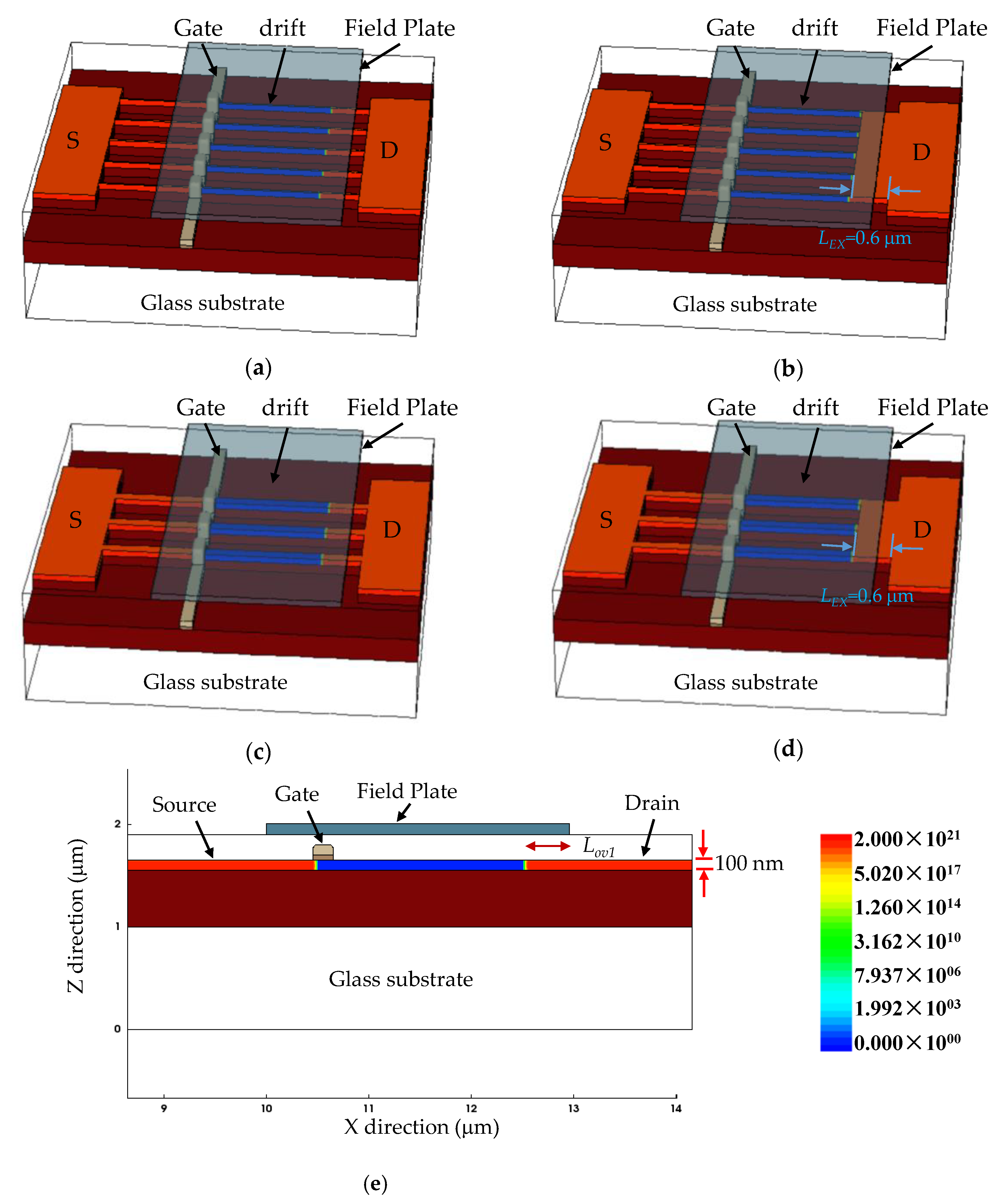
2. Materials and Methods
3. Results and Discussion
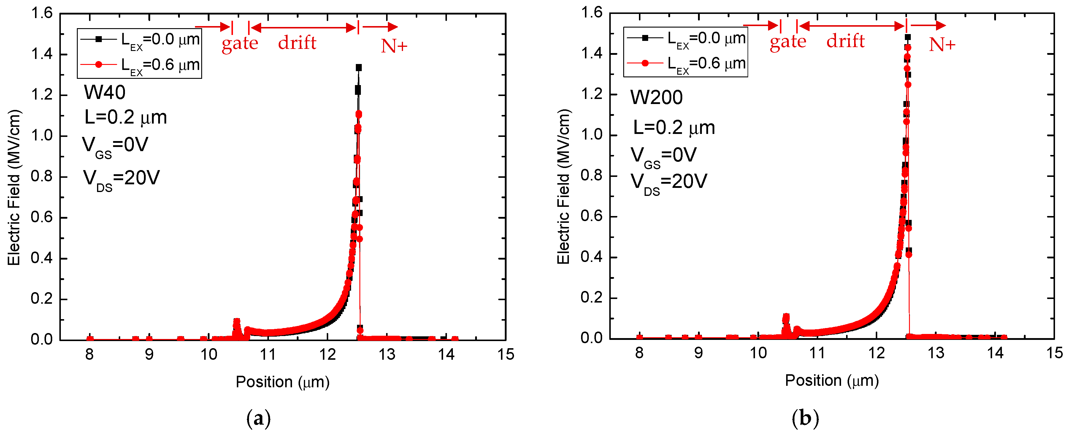
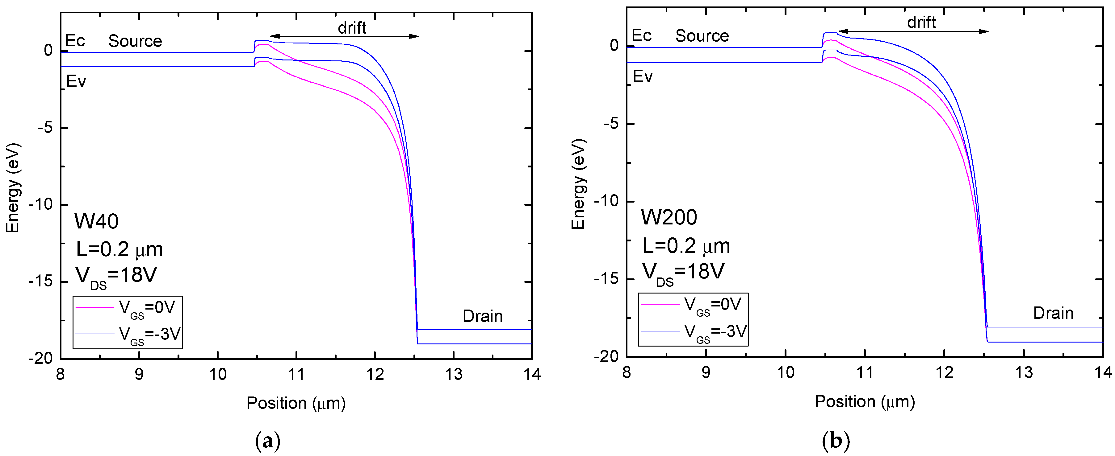
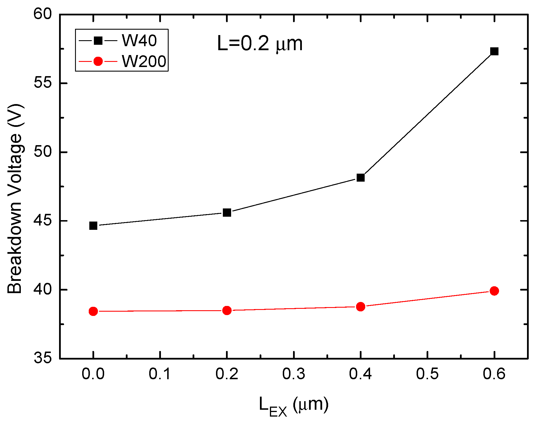
3.1. Breakdown Characteristics
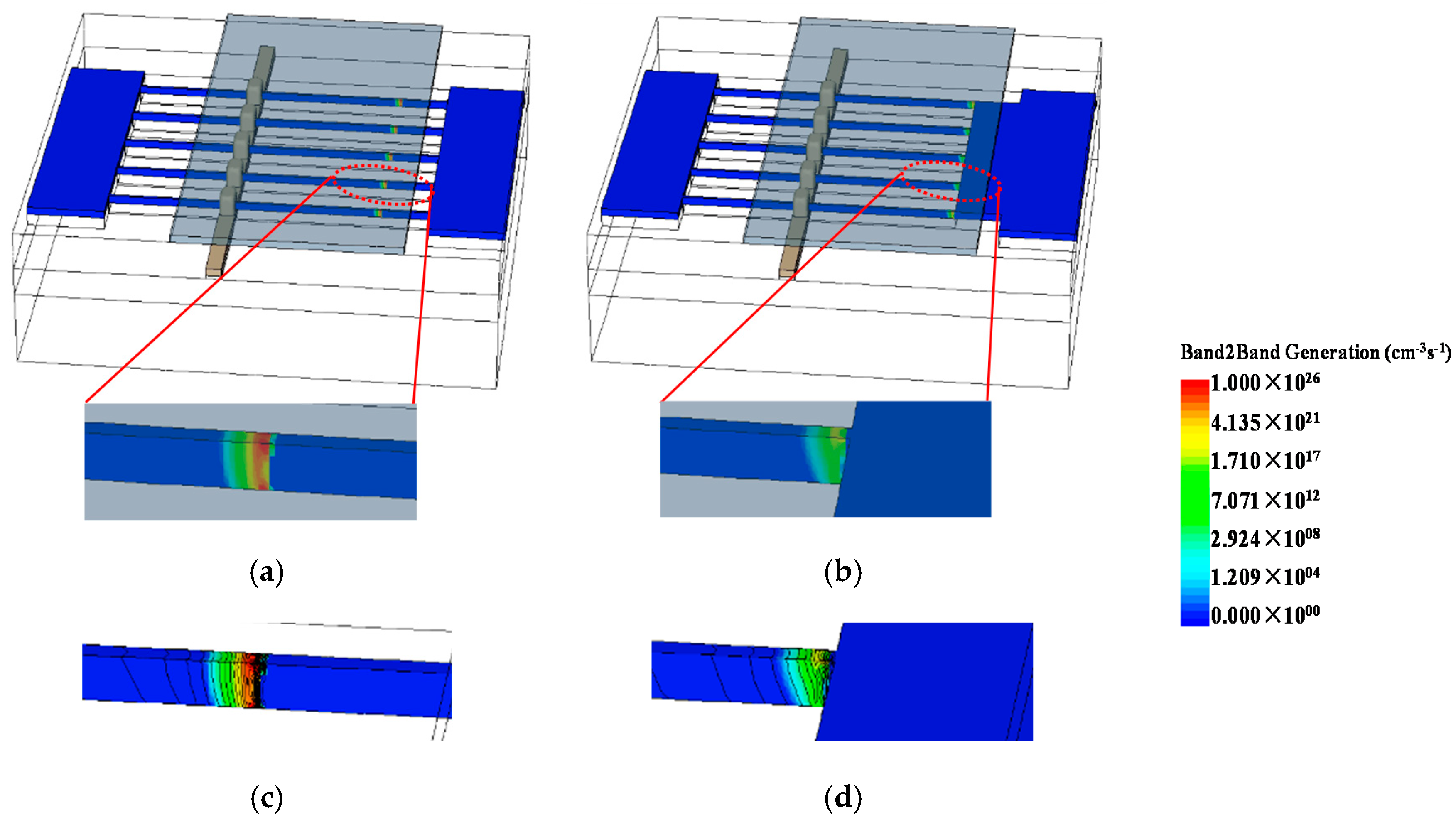
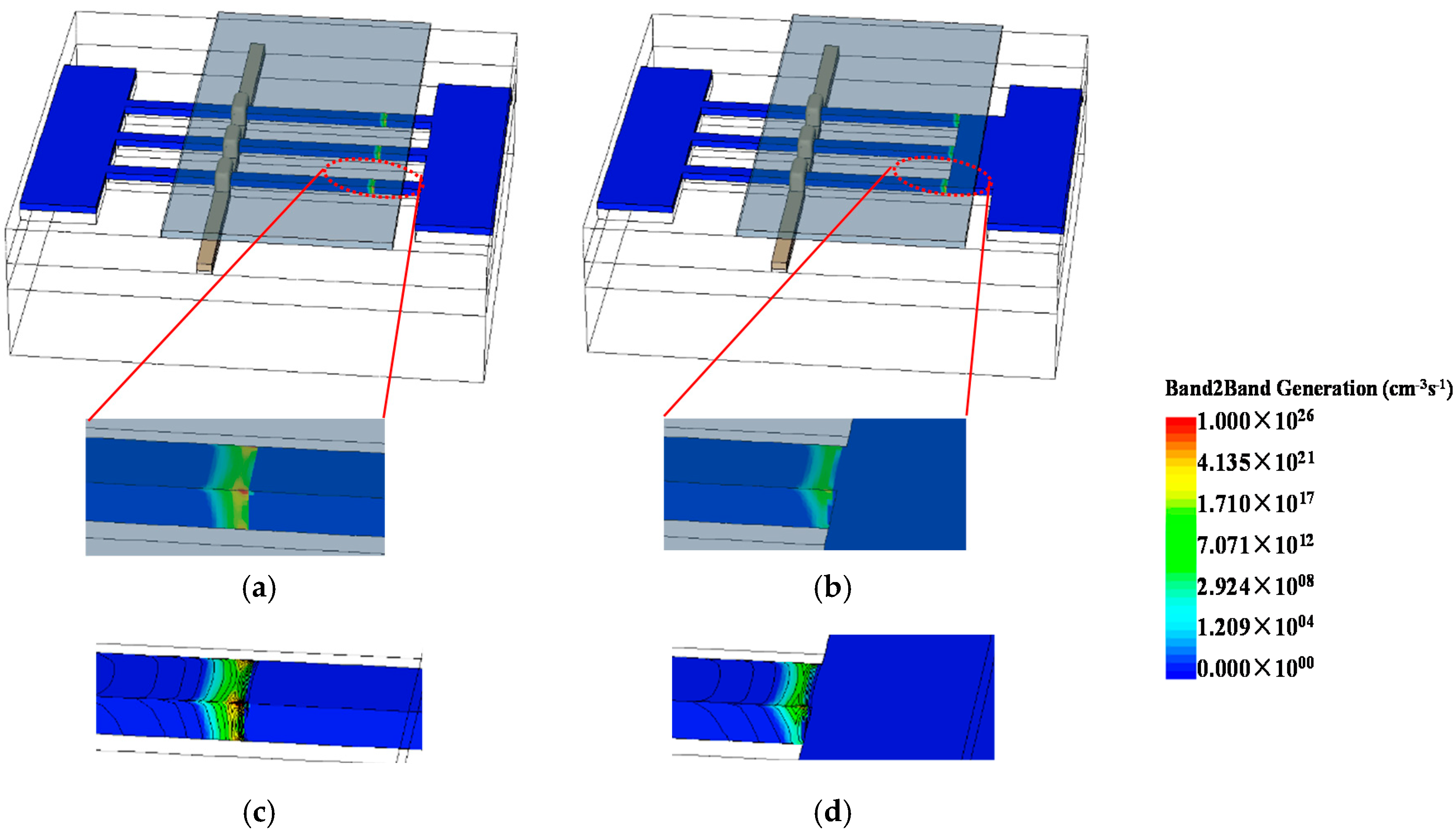
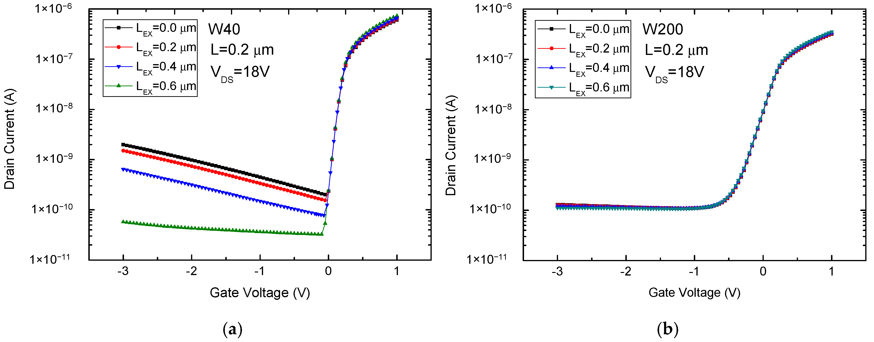
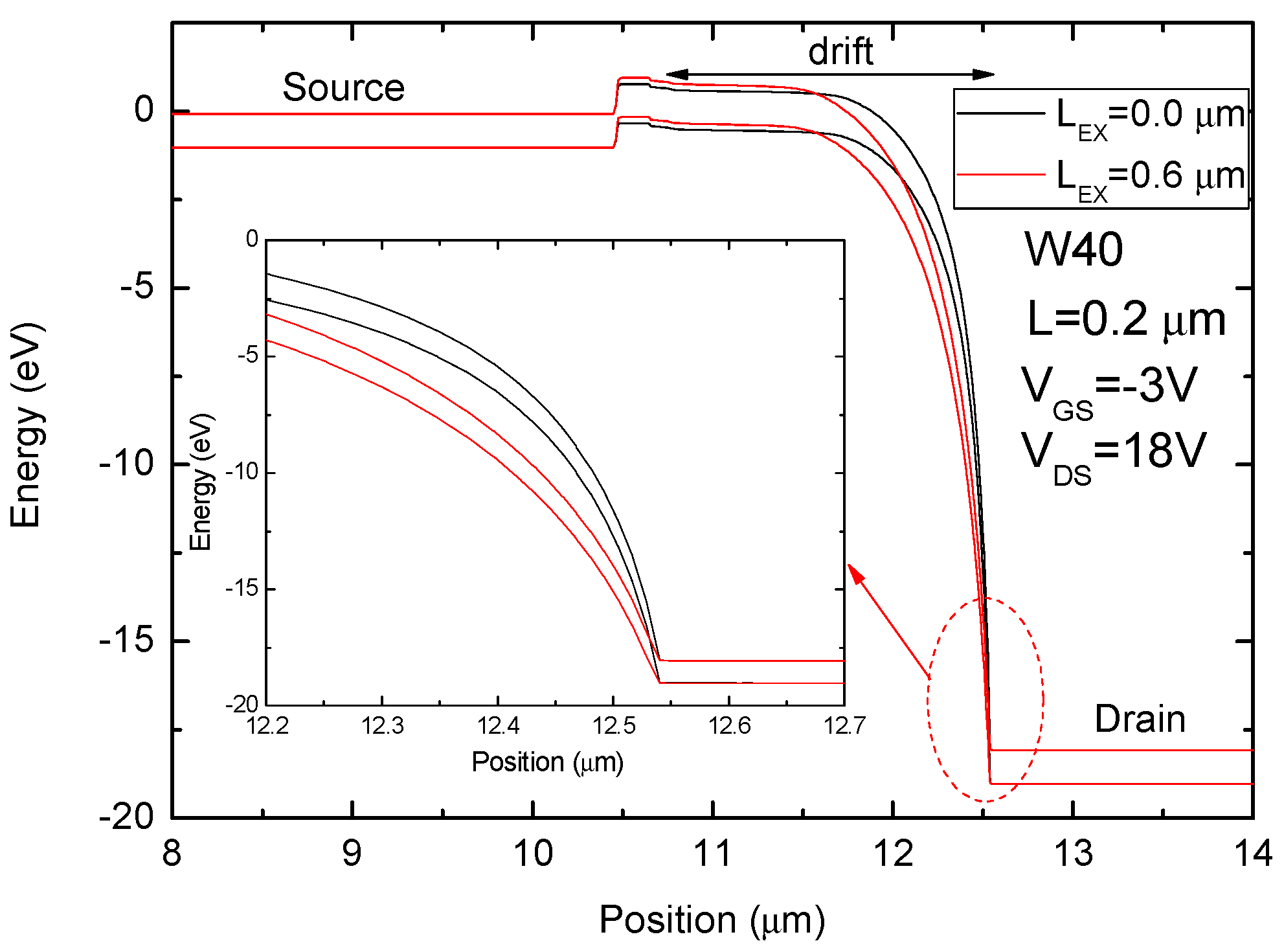
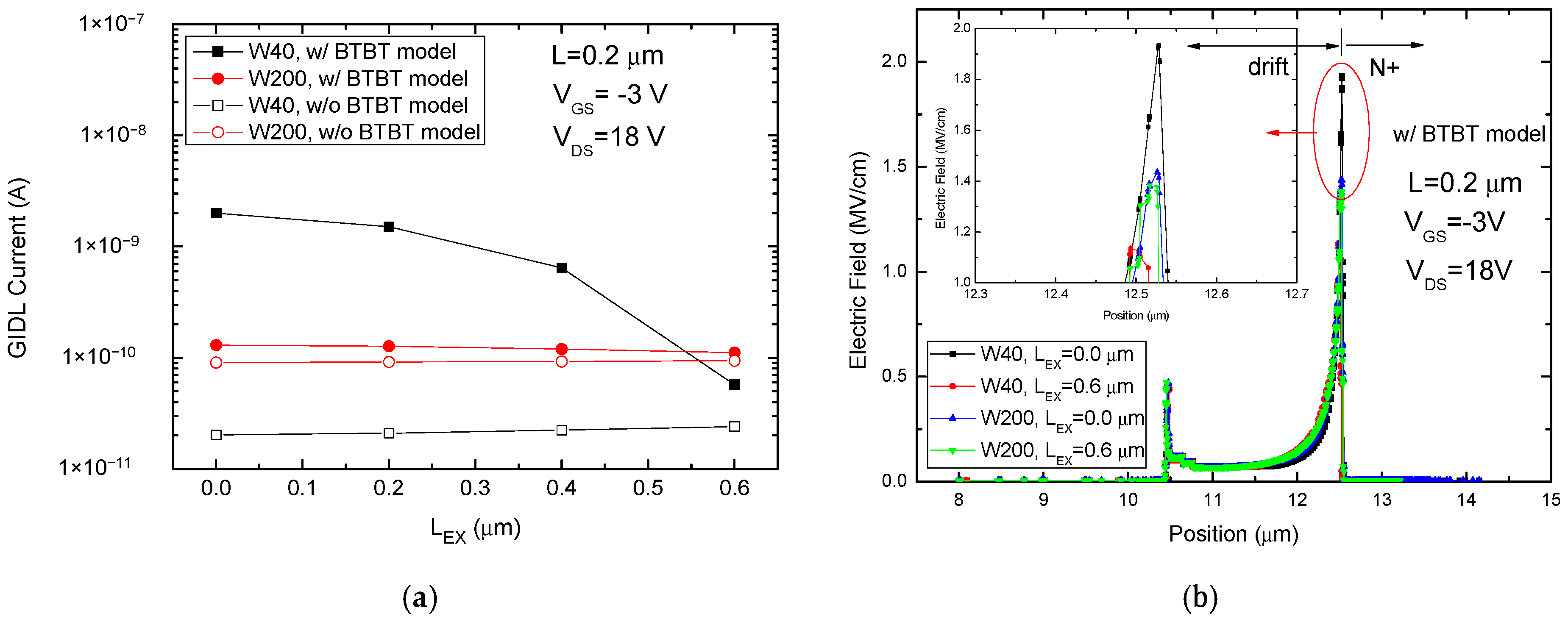
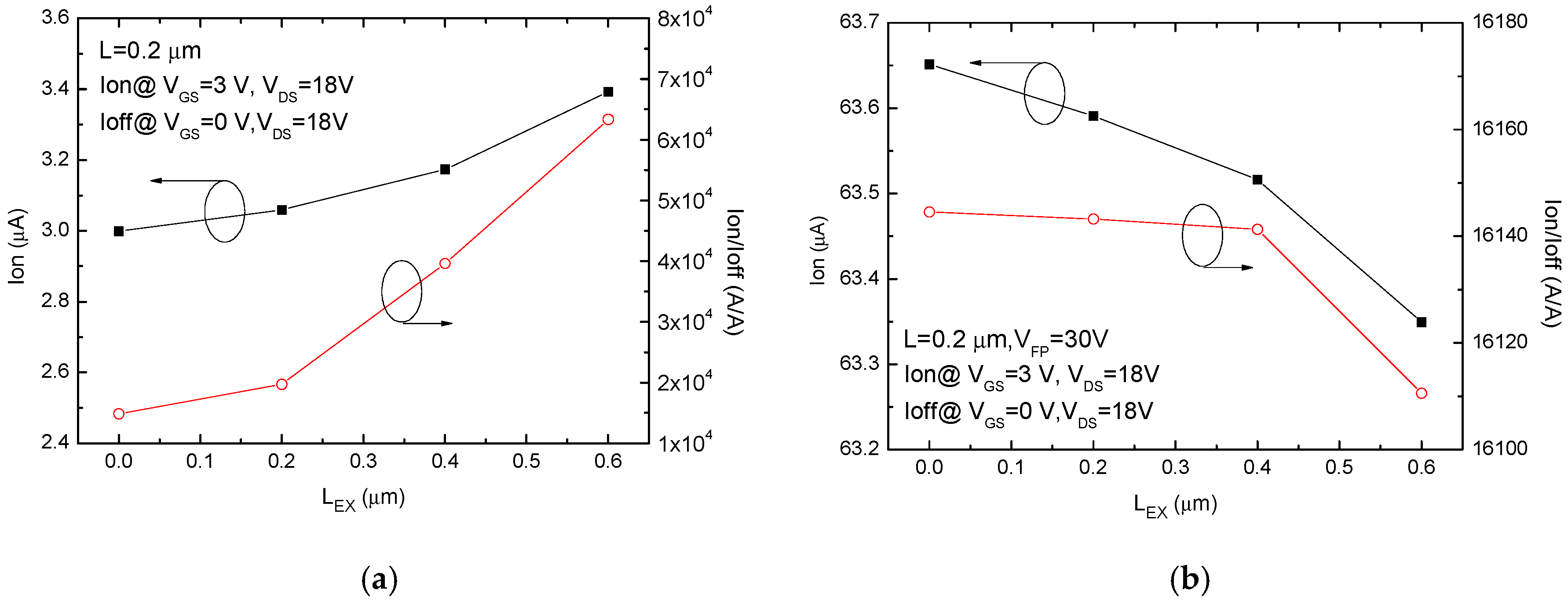
3.2. GIDL and ION/IOFF Ratio
4. Conclusions
Author Contributions
Funding
Acknowledgments
Conflicts of Interest
References
- Kuo, P.Y.; Lin, J.Y.; Chao, T.S. Implantation free GAA double spacer poly-Si nanowires channel junctionless FETs with sub-1V gate operation and near ideal subthreshold swing. In Proceedings of the IEEE IEDM, Washington, DC, USA, 7–9 December 2015; pp. 631–634. [Google Scholar] [CrossRef]
- Hung, M.F.; Wu, Y.C.; Tien, S.C.; Chen, J.H. Polycrystalline-Si TFT TANOS flash memory cell with Si nanocrystals for high program/erase speed and good retention. IEEE Electron Device Lett. 2012, 33, 649–651. [Google Scholar] [CrossRef]
- Chen, Y.J.E.; Lee, Y.J.; Yu, Y.H. Investigation of polysilicon thin-film transistor technology for RF applications. IEEE Trans. Microw. Theory Tech. 2010, 58, 3444. [Google Scholar] [CrossRef]
- Yu, Y.H.; Lee, Y.J.; Li, Y.H.; Kuo, C.H.; Li, C.H.; Hsieh, Y.J.; Liu, C.T.; Chen, Y.J.E. An LTPS TFT Demodulator for RFID Tags Embeddable on Panel Displays. IEEE Trans. Microw. Theory Tech. 2009, 57, 1356–1361. [Google Scholar] [CrossRef]
- Vidor, F.F.; Meyers, T.; Hilleringmann, U. Inverter circuits using ZnO nanoparticle based thin-film transistors for flexible electronic applications. Nanomaterials 2016, 6, 154. [Google Scholar] [CrossRef] [PubMed]
- Chen, K.N.; Yang, C.F.; Wu, C.C.; Chen, Y.H. Development of the α-IGZO/Ag/α-IGZO triple-layer structure films for the application of transparent electrode. Materials 2017, 10, 226. [Google Scholar] [CrossRef] [PubMed]
- Martins, J.; Bahubalindruni, P.; Rovisco, A.; Kiazadeh, A.; Martins, R.; Fortunato, E.; Barquinha, P. Bias stress and temperature impact on InGaZnO TFTs and circuits. Materials 2017, 10, 680. [Google Scholar] [CrossRef] [PubMed]
- Fan, C.L.; Tseng, F.P.; Tseng, C.Y. Electrical performance and reliability improvement of amorphous-indium-gallium-zinc-oxide thin-film transistors with HfO2 gate dielectrics by CF4 plasma treatment. Materials 2018, 11, 824. [Google Scholar] [CrossRef] [PubMed]
- Huang, T.Y.; Lewis, A.G.; Chiang, A.; Wu, I.W.; Koyanagi, M. A new implant-through-contact method for fabricating high-voltage TFTs. IEEE Electron Device Lett. 1988, 9, 347–349. [Google Scholar] [CrossRef]
- Hack, M.; Chiang, A.; Huang, T.Y.; Lewis, A.G.; Martin, R.A.; Tuan, H.; Wu, I.W.; Yap, P. High-voltage thin film transistors for large area microelectronics. In Proceedings of the IEEE IEDM, San Francisco, CA, USA, 11–14 December 1988; pp. 252–255. [Google Scholar] [CrossRef]
- Unagami, T.; Tsujiyama, B. High-voltage silicon thin film transistor on quartz. IEEE Electron Device Lett. 1982, 3, 167–168. [Google Scholar] [CrossRef]
- Tanaka, K.; Arai, H.; Kohda, S. Characteristics of offset-structure polycrystalline-silicon thin-film transistors. IEEE Electron Device Lett. 1988, 9, 23–25. [Google Scholar] [CrossRef]
- Clough, F.J.; Narayanan, E.M.S.; Chen, Y.; Eccleston, W.; Milne, W.I. Polycrystalline silicon thin film transistor incorporating a semi-insulating field plate for high voltage circuitry on glass. Appl. Phys. Lett. 1997, 71, 2002–2004. [Google Scholar] [CrossRef]
- Xu, Y.Z.; Clough, F.J.; Narayanan, E.M.S.; Chen, Y.; Milne, W.I. A conductivity modulated high voltage polycrystalline silicon thin film transistor with improved on state and transient performance. In Proceedings of the IEEE IEDM, San Francisco, CA, USA, 6–9 December 1998; pp. 273–276. [Google Scholar] [CrossRef]
- Huang, T.Y.; Wu, I.W.; Lewis, A.G.; Chiang, A.; Bruce, R.H. A simpler 100-V polysilicon TFT with improved turn-on characteristics. IEEE Electron Device Lett. 1990, 11, 244–246. [Google Scholar] [CrossRef]
- Kim, S.Y.; Loke, W.F.; Jung, B.; Roy, K. High-frequency modeling of poly-Si thin-film transistors for low-cost RF applications. IEEE Trans. Electron Devices 2012, 59, 2296–2301. [Google Scholar] [CrossRef]
- Oh, S.H.; Monroe, D.; Hergenrother, J.M. Analytic description of short-channel effects in fully-depleted Double-Gate and cylindrical, surrounding-gate MOSFETs. IEEE Electron Device Lett. 2000, 21, 445–447. [Google Scholar] [CrossRef]
- Chang, L.; Tang, S.; King, T.J.; Hu, C. Gate length scaling and threshold voltage control of double-gate MOSFETs. In Proceedings of the IEEE IEDM, San Francisco, CA, USA, 10–13 December 2000; pp. 719–722. [Google Scholar] [CrossRef]
- Hisamoto, D.; Lee, W.; Kedzierski, J.; Takeuchi, H.; Asano, K.; Kuo, C.; Anderson, E.; King, T.J.; Bokor, J.; Hu, C. FinFET—a self-aligned double-gate MOSFET scalable to 20 nm. IEEE Trans. Electron Device 2000, 12, 2320–2325. [Google Scholar] [CrossRef]
- Rios, R.; Cappellani, A.; Armstrong, M.; Budrevich, A.; Gomez, H.; Pai, R.; Rahhal-orabi, N.; Kuhn, K. Comparison of junctionless and conventional trigate transistors with Lg down to 26 nm. IEEE Electron Device Lett. 2011, 32, 1170–1172. [Google Scholar] [CrossRef]
- Barraud, S.; Berthomé, M.; Coquand, R.; Cassé, M.; Ernst, T.; Samson, M.P.; Perreau, P.; Bourdelle, K.K.; Faynot, O.; Poiroux, T. Scaling of trigate junctionless nanowire MOSFET with gate length down to 13 nm. IEEE Electron Device Lett. 2012, 33, 12251227. [Google Scholar] [CrossRef]
- Liao, T.C.; Tu, S.W.; Yu, M.H.; Lin, W.K.; Liu, C.C.; Chang, K.J.; Tai, Y.H.; Cheng, H.C. Novel gate-all-around poly-Si TFTs with multiple nanowire channels. IEEE Electron Device Lett. 2008, 29, 889. [Google Scholar] [CrossRef]
- Lu, Y.H.; Kuo, P.Y.; Wu, Y.H.; Chen, Y.H.; Chao, T.S. NoNovel sub-10-nm gate-all-around Si nanowire channel poly-Si TFTs with raised source/drain. IEEE Electron Device Lett. 2011, 32, 173–175. [Google Scholar] [CrossRef]
- Narimani, K.; Trellenkamp, S.; Tiedemann, A.; Mantl, S.; Zhao, Q.T. Strained silicon single nanowire gate-all-around TFETs with optimized tunneling junctions. Appl. Sci. 2018, 8, 670. [Google Scholar] [CrossRef]
- Chen, J.; Chan, T.Y.; Chen, I.C.; Ko, P.K.; Hu, C. Subbreakdown drain leakage current in MOSFET. IEEE Electron Device Lett. 1987, 11, 515–517. [Google Scholar] [CrossRef]
- Chan, T.Y.; Chen, J.; Ko, P.K.; Hu, C. The impact of gate-induced leakage current on MOSFET scaling. In Proceedings of the IEEE IEDM, Washington, DC, USA, 6–9 December 1987; pp. 718–721. [Google Scholar]
- Wann, H.; Ko, P.K.; Hu, C. Gate-induced band-to-band tunneling leakage current in LDD MOSFETs. In Proceedings of the IEEE IEDM, San Francisco, CA, USA, 13–16 December 1992; pp. 147–150. [Google Scholar]
- Fan, J.; Li, M.; Xu, X.; Huang, R. New observation on gate-induced drain leakage in Silicon nanowire transistors with Epi-Free CMOS compatible technology on SOI substrate. In Proceedings of the IEEE SOI-3D-Subthreshold Microelectronics Technology Unified Conference (S3S), Monterey, CA, USA, 7–10 October 2013; pp. 1–2. [Google Scholar]
- Fan, J.; Ming, L.; Xiaoyan, X.; Yuancheng, Y.; Haoran, X.; Ru, H. Insight Into gate-induced drain leakage in silicon nanowire transistors. IEEE Trans. Electron Device 2015, 62, 213–219. [Google Scholar]
- Sahay, S.; Kumar, M.J. A novel gate-stack-engineered nanowire FET for scaling to the sub-10-nm regime. IEEE Trans. Electron Device 2016, 63, 5055–5059. [Google Scholar] [CrossRef]
- Sahay, S.; Kumar, M.J. Insight into lateral band-to-band-tunneling in nanowire junctionless FETs. IEEE Trans. Electron Device 2016, 63, 4138–4142. [Google Scholar] [CrossRef]
- Hur, J.; Lee, B.H.; Kang, M.H.; Ahn, D.C.; Bang, T.; Jeon, S.B. Comprehensive analysis of gate-induced drain leakage in vertically stacked nanowire FETs: inversion-mode versus junctionless mode. IEEE Electron Device Lett. 2016, 37, 541–544. [Google Scholar] [CrossRef]
- Sahay, S.; Kumar, M.J. Spacer design guidelines for nanowire FETs from gate-induced drain leakage perspective. IEEE Trans. Electron Device 2017, 64, 3007–3015. [Google Scholar] [CrossRef]
- Sahay, S.; Kumar, M.J. Physical insights into the nature of gate-induced drain leakage in ultrashort channel nanowire FETs. IEEE Trans. Electron Device 2017, 64, 2604–2610. [Google Scholar] [CrossRef]
- Tsai, J.Y.; Hu, H.H.; Wu, Y.C.; Jhan, Y.R.; Chen, K.M.; Huang, G.W. A novel hybrid poly-Si nanowire LDMOS with extended drift. IEEE Electron Device Lett. 2014, 35, 366–368. [Google Scholar] [CrossRef]
- Tsai, J.Y.; Hu, H.H. Novel gate-all-around high-voltage thin-film transistor with t-shaped metal field plate design. IEEE Trans. Electron Device 2015, 62, 882–887. [Google Scholar] [CrossRef]
- Auth, C.; Cappellani, A.; Chun, J.; Dalis, A.; Davis, A.; Ghani, T.; Glass, G.; Glassman, T.; Harper, M.; Hattendorf, M. 45 nm high-K metal gate strain-enhanced transistors. In Proceedings of the Symposium on VLSI Technology, Honolulu, HI, USA, 17–19 June 2008; pp. 128–129. [Google Scholar]
- Kesapragada, S.; Wang, R.; Liu, D.; Liu, G.; Xie, Z.; Ge, Z.; Yang, H.; Lei, Y.; Lu, X.; Tang, X.; et al. High-k/metal gate stacks in gate first and replacement gate schemes. In Proceedings of the IEEE/SEMI Advanced Semiconductor Manufacturing Conference (ASMC), San Francisco, CA, USA, 11–13 July 2010; pp. 256–259. [Google Scholar]
- Jan, C.H.; Agostinelli, M.; Deshpande, H.; El-Tanani, M.A. RF CMOS technology scaling in high-k/metal gate era for RF SoC (system-on-chip) applications. In Proceedings of the IEEE International Electron Devices Meeting, San Francisco, CA, USA, 6–8 December 2010; pp. 604–607. [Google Scholar]
- Duan, F.L.; Zhao, X.; Ioannou, D.E. Increased channel edge impact ionization in SOI MOSFET’s and effects on device operation. In Proceedings of the IEEE International SOI Conference Proceedings, Stuart, FL, USA, 5–8 October 1998; pp. 171–172. [Google Scholar]
- Lee, C.W.; Afzalian, A.; Yan, R.; Akhavan, N.D.; Xiong, W.; Colinge, J.P. Drain breakdown voltage in MuGFETs: Influence of physical parameters. IEEE Trans. Electron Device 2008, 55, 3503–3506. [Google Scholar] [CrossRef]
- Chen, K.M.; Chen, B.Y.; Chiu, C.S.; Huang, G.W.; Chen, C.H.; Lin, H.C.; Huang, T.Y.; Chen, M.Y.; Yang, Y.C.; Jaw, B.; et al. Performance improvement in RF LDMOS transistors using wider drain contact. IEEE Electron Device Lett. 2013, 34, 1085–1087. [Google Scholar] [CrossRef]


© 2018 by the authors. Licensee MDPI, Basel, Switzerland. This article is an open access article distributed under the terms and conditions of the Creative Commons Attribution (CC BY) license (http://creativecommons.org/licenses/by/4.0/).
Share and Cite
Hu, H.-H.; Zeng, Y.-W.; Chen, K.-M. Improving the Gate-Induced Drain Leakage and On-State Current of Fin-Like Thin Film Transistors with a Wide Drain. Appl. Sci. 2018, 8, 1406. https://doi.org/10.3390/app8081406
Hu H-H, Zeng Y-W, Chen K-M. Improving the Gate-Induced Drain Leakage and On-State Current of Fin-Like Thin Film Transistors with a Wide Drain. Applied Sciences. 2018; 8(8):1406. https://doi.org/10.3390/app8081406
Chicago/Turabian StyleHu, Hsin-Hui, Yan-Wei Zeng, and Kun-Ming Chen. 2018. "Improving the Gate-Induced Drain Leakage and On-State Current of Fin-Like Thin Film Transistors with a Wide Drain" Applied Sciences 8, no. 8: 1406. https://doi.org/10.3390/app8081406
APA StyleHu, H.-H., Zeng, Y.-W., & Chen, K.-M. (2018). Improving the Gate-Induced Drain Leakage and On-State Current of Fin-Like Thin Film Transistors with a Wide Drain. Applied Sciences, 8(8), 1406. https://doi.org/10.3390/app8081406