Article

Influence of Substrate Modification with Dipole Monolayers on the Electrical Characteristics of Short-Channel Polymer Field-Effect Transistors

1
Department of Physics and Electronics, Osaka Prefecture University, Sakai 599-8531, Japan
2
The Research Institute for Molecular Electronic Devices, Osaka Prefecture University, Sakai 599-8531, Japan
3
Advanced ICT Research Institute, National Institute of Information and Communications Technology, Kobe 651-2492, Japan
*
Authors to whom correspondence should be addressed.
Appl. Sci. 2018, 8(8), 1274; https://doi.org/10.3390/app8081274
Submission received: 29 June 2018 / Revised: 17 July 2018 / Accepted: 26 July 2018 / Published: 1 August 2018
(This article belongs to the Special Issue Semiconducting Polymer for Organic Transistors)

Abstract

:
This study investigates the influence of self-assembled monolayer treatment of gate insulators on the electrical characteristics of bottom-gate/bottom-contact organic field-effect transistors (OFETs) with short channel lengths of 5 μm to 30 nm. The treatment of 3-chloropropyltrichlorosilane (CPTS) with large dipoles produces a high built-in electric field perpendicular to the SiO2 gate insulator surface, which results in a threshold voltage shift and enhanced hole injection compared to the treatment of phenethyltrichlorosilane (PETS) with small dipoles. Pronounced parabolic drain current‒voltage (IDVD) characteristics due to a space-charge limited current are observed in short-channel OFETs based on poly(3-hexylthiophene) with CPTS-treated gate insulators. CPTS treatment on short-channel OFETs based on poly(9,9-dioctylfluorene-co-bithiophene) (F8T2) suppresses the nonlinear ID increase in the low VD region caused by the voltage drop at the Au/F8T2 contact. The influence of the increase in the net source-drain electric field associated with the reduced voltage drops on the channel-length dependence of the field-effect mobility of short-channel F8T2 FETs is also discussed.

Graphical Abstract

1. Introduction

There has been considerable interest in the development of organic field-effect transistors (OFETs) with high electrical performance because of their potential use in various organic devices, such as flexible displays, low-cost radio frequency identification tags, and large-area sensors [1,2,3]. Shrinking the channel length (L) of OFETs, which is typically several tens of micrometers, is a crucial issue for enhancing the performances of electronic circuits based on OFET devices because the operational speed and output current of FET devices are, respectively, proportional to μ/L2 and μ/L, where μ is the field-effect mobility. However, reducing L to the sub-micrometer regime generally suffers from the high space-charge limited current (SCLC) associated with the application of a high source-drain electric field to the organic semiconductor; this results in parabolic drain current‒drain voltage (IDVD) characteristics without current saturation and an increase in the off current [4,5,6,7,8]. Such short-channel effects in OFETs have been reported to be suppressed by using ultrathin gate insulators (several nanometers in thickness) [9] to ensure a gradual-channel approximation (the gate electric field in the channel is much larger than the source-drain electric field) [4,10].
We have previously studied the influence of the source electrode/organic semiconductor contact on the current–voltage characteristics of short-channel OFETs based on p-type organic semiconductors and reported that the parabolic IDVD characteristics and high off current are suppressed by using organic semiconductors with high ionization potentials [11]. This behavior originates in the formation of Schottky barriers for hole injection at the source electrode/organic semiconductor contact, which reduces the SCLC and increases the effectiveness of the gate electric field in the channel because of the decrease in the net source-drain electric field. However, the formation of charge injection barriers also causes an increase in the threshold voltage of the short-channel OFETs and nonlinear ID increase in the low VD region. It has been reported that the threshold voltage of OFETs can be reduced by increasing the capacitance of gate insulators [12,13] and modifying the surfaces of gate insulators (next to the organic semiconductor channels) with self-assembled monolayers (SAMs) having polar end groups [14,15,16,17,18,19,20]. In particular, the latter approach uses a built-in electric field produced by the permanent dipoles of SAMs, which can provide an effective route to reduce the threshold voltage of short-channel OFETs without thinning the gate insulator to several nanometers.
In this study, we investigate the influence of the surface treatment of gate insulators with dipole SAMs on the electrical characteristics of short-channel OFETs with L of 5 μm to 30 nm fabricated using p-type polymer semiconductors with different ionization potentials.

2. Experimental

Figure 1a shows a schematic cross-section of the short-channel OFETs fabricated in this study. We used a heavily doped n-type Si wafer with a thermally-grown SiO2 insulating layer (200 or 50 nm thick), which served as the gate electrode and gate insulator, respectively. Ti/Au (1–2 nm/30 nm) source-drain electrodes with different values of L (5 μm to 30 nm) were fabricated on the Si/SiO2 substrates by using electron-beam lithography and a lift-off process. The bottom Ti layer was employed to promote the adhesion of the Au electrodes to the SiO2 surface. To ensure that carriers can be injected from the Au source electrode into the organic semiconductor layer [21], the thin Ti adhesion layer was used in our devices. The channel width (W) was scaled to maintain W/L = 10 to adjust the dimension of the output current in devices with different L.
Figure 1b shows the chemical structures of organosilanes used to form dipole SAMs on the SiO2 surfaces. We used phenethyltrichlorosilane (PETS) and 3-chloropropyltrichlorosilane (CPTS), which have different polarities of dipole moments and form SAMs with similar levels of hydrophobicity [15,16]. CPTS has a large dipole moment pointing from chlorine toward trichlorosilane; this forms strong electron-withdrawing surfaces and leads to the accumulation of holes [15,16,18,22]. PETS has a relatively small dipole moment pointing toward the phenyl end group [16,23,24], which can form weak electron-donating surfaces. After the Si/SiO2 substrates with Ti/Au source-drain electrodes were cleaned with acetone and isopropanol in an ultrasonic bath and with an UV/O3 cleaner, the substrates were immersed in ~10 mM toluene solutions of the organosilanes in capped bottles for ~14 h to form SAMs on the SiO2 surfaces. After SAMs were formed, the substrates were washed ultrasonically with fresh toluene, acetone, and isopropanol to remove any excessive layers and then baked at 150 °C for 1 h in a vacuum to enhance the cross-linking of the organosilane molecules. The water contact angles of the Si/SiO2 substrates treated with PETS and CPTS SAMs were 92° and 84°, respectively.
For the organic semiconductors, we used p-type polymer semiconductors with different ionization potentials (IPs), as shown in Figure 1c: regioregular poly(3-hexylthiophene) (P3HT) (IP = 4.9 eV) and poly(9,9-dioctylfluorene-co-bithiophene) (F8T2) (IP = 5.5 eV) [25]. The organic semiconductor films were deposited on the SAM-treated Si/SiO2 substrates by spin-coating from 0.5–1 wt % toluene solutions. The obtained films were followed by thermal annealing in a vacuum to remove residual solvent and dopants such as oxygen and water from the semiconductor films [26]. The annealing temperature of 100 °C was used to avoid the degradation of field-effect mobility in P3HT FETs caused by high-temperature annealing [27].
The electrical measurements of the fabricated OFET devices were performed in a vacuum at a probe station (Lake Shore Cryotronics TTP4 (Westerville, OH, USA)) by using source meters (Keithley 2611 and 2400 (Cleveland, OH, USA)) at room temperature. The field-effect mobility (μ) was calculated from the transfer characteristics in the saturation region by using the following standard FET equation:
  I D =   μ C i W 2 L ( V G V t h ) 2  
where Ci is the capacitance per unit area for the gate insulator, VG is the gate voltage, and Vth is the threshold voltage.

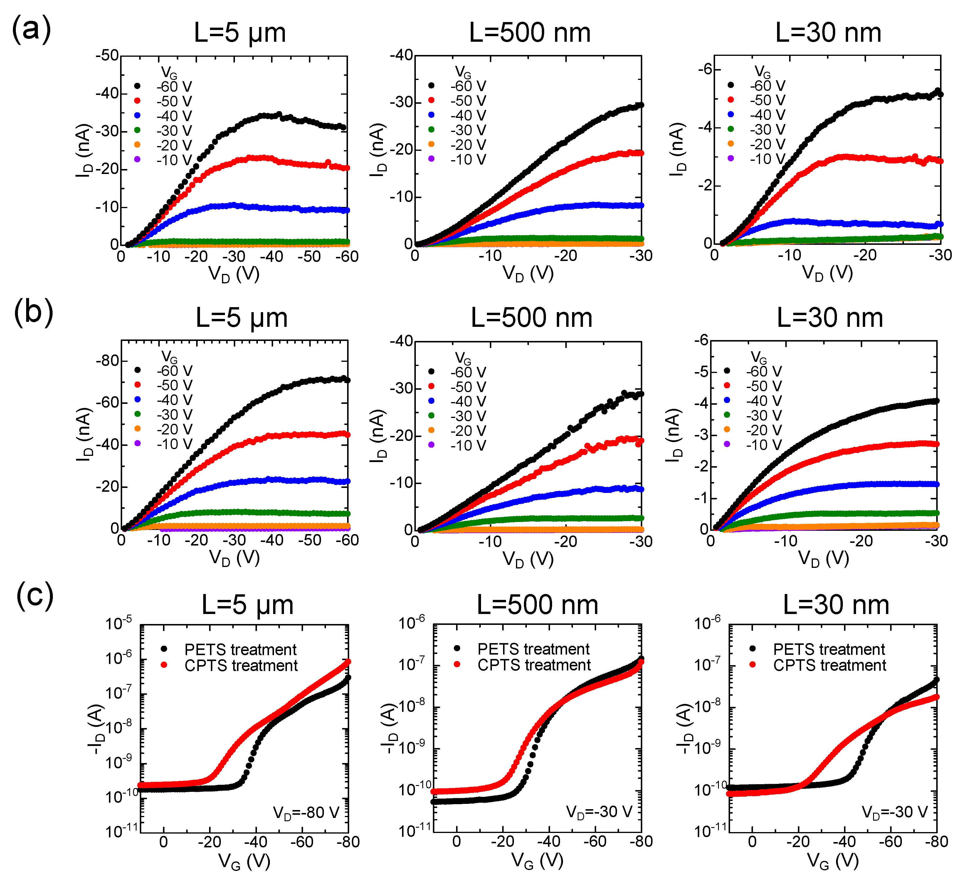
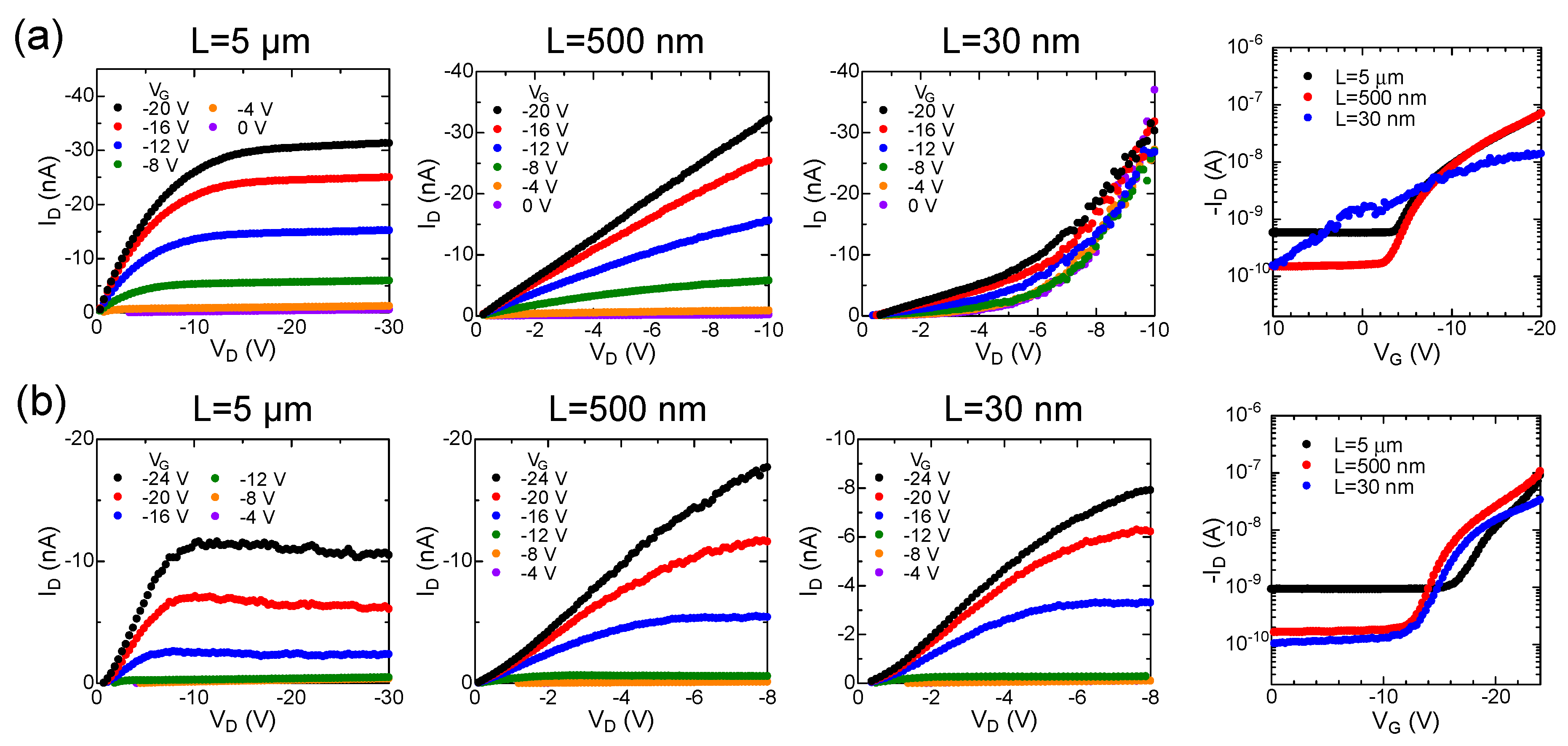
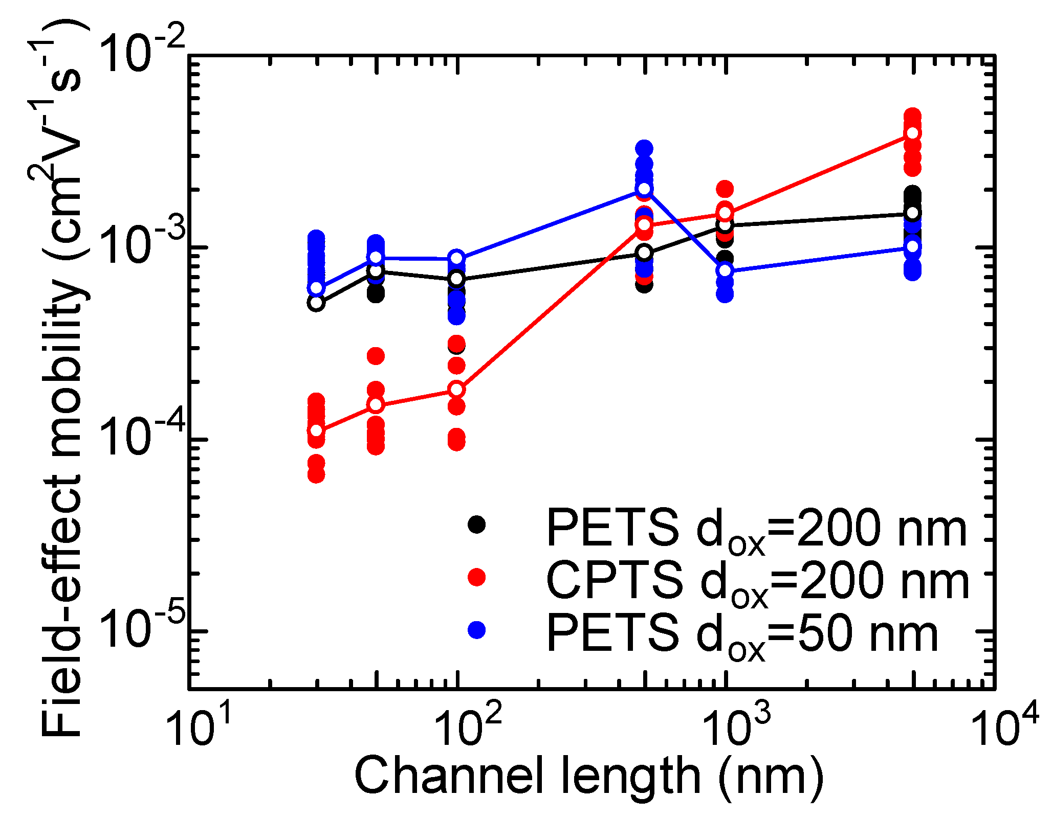
3. Results and Discussion

Figure 2a,b show the typical IDVD (output) characteristics of short-channel P3HT-based FETs with L of 5 μm, 500 nm, and 30 nm fabricated on 200-nm-thick SiO2 insulators treated with PETS and CPTS SAMs, respectively. The P3HT FETs with L = 5 μm show typical output characteristics with clear current saturation. This can be attributed to the high gate electric field relative to the source-drain electric field, which ensures that the gate electric field determines the charge distribution within the channel (i.e., the gradual-channel approximation) [4,10]. As the channel length is reduced to the sub-micrometer regime, the output characteristics become parabolic, and the drain current at VG = 0 V increases. Such behavior has been explained by the increase in the current flow to the bulk region of the organic semiconductor due to the SCLC [28]. The P3HT semiconductor allows forming ohmic contacts with the Au source-drain electrodes because of the small potential difference between the work function of Au (4.8 eV) and the ionization potential of P3HT (4.9 eV) [29]. Applying the source-drain voltage to the sub-micrometer channel leads to an extremely high source-drain electric field, which results in the SCLC significantly contributing to the drain current.
Figure 2c shows the IDVG (transfer) characteristics of the short-channel P3HT FETs with PETS- and CPTS-treated SiO2 gate insulators. The transfer characteristics of the devices with CPTS-treated gate insulators shift toward the positive VG direction compared to that with PETS-treated gate insulators. Such behavior is consistent with the results reported for pentacene-based OFETs with L = 30–150 μm on SAM-treated SiO2 insulators [15,16] and has been explained by the change in surface potential of the gate insulator by the permanent dipole of SAMs [14,15,16,17,18,19,20]. As shown in Figure 3, the electric field pointing toward the surface of the gate insulator produced by the dipole moment of CPTS causes the bending of molecular orbital levels of organic semiconductors toward high energy. The upward bending of energy levels accumulates additional holes in the channel, which leads to the positive shift of transfer characteristics [15,16].
The field-effect mobility of the P3HT FET devices with L = 5 μm on the CPTS-treated gate insulators was 6.8 ± 0.81 × 10⁻⁴ cm2 V−1 s−1, which was slightly lower than that of the devices on the PETS-treated gate insulators (1.4 ± 0.13 × 103 cm2 V1 s1). Such a decrease in the mobility of P3HT FETs might be attributed to the smaller water contact angle of CPTS-treated gate insulators, since the ordering of organic semiconducting molecules in bottom-gate OFETs depends largely on the surface energy of gate insulators and a more hydrophobic surface gives a higher mobility [30,31]. It can be seen in the figures that the off current of the devices with CPTS-treated gate insulators remarkably increases as the channel length is reduced to 30 nm. Additionally, the devices with CPTS-treated gate insulators show a smaller increase in the drain current for the variation of the gate voltage, compared to the devices with PETS-treated gate insulators. These results clearly indicate that short-channel effects are more pronounced in the short-channel P3HT FETs fabricated on CPTS-treated gate insulators. This can be attributed to the improved injection of holes associated with the enhanced hole accumulation by CPTS SAMs, which increases the SCLC and reduces the modulation of the drain current by the gate voltage [8,9].
Figure 4 shows the output and transfer characteristics of short-channel F8T2-based FETs with L = 5 μm, 500 nm, and 30 nm that were fabricated on 200-nm-thick SiO2 gate insulators treated with PETS and CPTS SAMs. In contrast to the P3HT FETs, the short-channel F8T2 FETs exhibit no parabolic output characteristics when the channel length is reduced, and the saturation of drain current is clearly observed in F8T2 FETs with L = 30 nm despite the use of thick SiO2 gate insulators (200 nm). These results are attributed to the formation of Schottky barriers for hole injection because of the large potential difference between the work function of the source Au electrodes (4.8 eV) and ionization potential of the F8T2 semiconductors (5.5 eV) [29], which leads to contact-limited charge transport and, hence, suppresses the SCLC. The formation of Schottky barriers also causes the voltage drop at the source electrode/organic semiconductor contact, which reduces the net source-drain electric field at the channel region. The resulting increased effectiveness of the gate electric field at the channel region has been shown to enhance the current modulation in OFETs with nanometer channels [8,9,11].
It can be seen in Figure 4a,b that the large voltage drop at the Au/F8T2 contact causes a nonlinear increase in ID in the low VD region in the F8T2 FETs with PETS-treated gate insulators, whereas the nonlinearity of the IDVD characteristics is decreased for short-channel F8T2 FETs with CPTS-treated gate insulators. These results are consistent with those observed for the short-channel P3HT FETs of Figure 2, which clearly indicates that a shift in the threshold voltage of transfer characteristics by CPTS SAMs involves the hole injection barriers at the source electrode/organic semiconductor interface being lowered. Such effects can manifest as the smaller modulation of the drain current by the gate voltage in F8T2 FETs with CPTS-treated gate insulators. This is because a lower hole injection barrier leads to a higher source-drain electric field and prevents the effective application of the gate electric field to the channel.
To clarify the difference in effects of the built-in electric field produced by the dipole SAM and increased gate electric field with thinner gate insulators, we investigated the electrical characteristics of short-channel P3HT and F8T2 FETs fabricated on thinner SiO2 insulators (50 nm thick) treated with the PETS SAMs (Figure 5). As shown in Figure 5a, P3HT FETs with L = 5 μm fabricated on 50-nm-thick gate insulators exhibit clearer current saturation behavior compared to devices on 200-nm-thick gate insulators (Figure 2a). Further, linear IDVD characteristics in the low VD region are obtained even for the device with L = 500 nm because of the increased gate electric field. Since OFETs require thin gate insulators (the thickness of a gate insulator is typically <L/10) to suppress the short-channel effects [4], P3HT FETs with L = 30 nm exhibit parabolic IDVD characteristics even when 50-nm-thick SiO2 insulators are used. For the F8T2 FETs shown in Figure 5b, good transistor characteristics with saturation of the drain current are observed in devices with L = 30 nm. This results from the formation of voltage drops at electrode contacts, as mentioned above. In contrast to the F8T2 FETs on 200-nm-thick gate insulators treated with CPTS SAMs (Figure 4b), the short-channel F8T2 FETs on 50-nm-thick gate insulators treated with PETS SAMs still exhibit a nonlinear increase in the drain current in the low-VD region. The strength of the built-in electric field produced by the dipole SAMs has been reported to be on the order of 1–10 MV cm−1 [14,15,16,17,32,33], which is comparable to the gate electric field induced by applying gate voltages of 20–200 V for the 200-nm-thick SiO2 gate insulator and 5–50 V for the 50-nm-thick SiO2 gate insulators. Therefore, a similar degree of improvement in charge injection is expected in devices with thinner gate insulators. These results clearly show that using gate insulators modified with dipole SAMs is effective not only for increasing the threshold voltage, but also for reducing the charge injection barriers at the source electrode/organic semiconductor contacts of short-channel OFETs.
Figure 6 shows the channel-length dependence of the field-effect mobilities of F8T2 FETs fabricated on PETS- and CPTS-treated SiO2 gate insulators with different thicknesses (dox). In all devices, the field-effect mobility decreases with the channel length. Similar dependences have typically been observed in OFETs and explained by the increased influence of the contact resistance on the channel resistance [34]. This apparently reduces the field-effect mobility calculated with Equation (1). Therefore, the improved charge injection of F8T2 FETs by the CPTS treatment of gate insulators is expected to increase the field-effect mobility of short-channel F8T2 FETs. In fact, the devices with L = 5 μm formed on CPTS-treated gate insulators exhibited higher mobility (3.9 ± 0.77 × 103 cm2 V1 s1) than those formed on PETS-treated gate insulators (1.5 ± 0.30 × 103 cm2 V1 s1), as observed in Figure 6. The influence of the CPTS treatment on the mobility of F8T2 FETs is different from that of P3HT FETs shown in Figure 2, which can result from the larger influence of contact resistances on the field-effect mobility of F8T2 FETs [29]. However, the field-effect mobility of the devices with CPTS-treated gate insulators shows a larger decrease as the channel length is reduced to the nanometer scale, as compared to those with PETS-treated gate insulators. Such behavior can be related to the smaller modulation of the drain current by the gate voltage observed in the F8T2 FETs with L = 30 nm by the CPTS treatment (Figure 4b). The results strongly suggest that the increased net source-drain electric field caused by the decreased voltage drop at the Au/F8T2 contact by the CPTS treatment reduces the effectiveness of the gate electric field in the channel, and it also leads to the apparent decrease in the field-effect mobility of OFETs with nanometer channels. Optimizing the dipole moments of SAM materials and using high-k gate dielectrics can further improve the field-effect mobility of nanochannel OFETs.

4. Conclusions

We have investigated the electrical characteristics of short-channel OFETs based on polymer semiconductors with different ionization potentials formed on SiO2 gate insulators treated with dipole SAMs. The built-in electric field produced by CPTS SAMs shifts the threshold voltage and reduces hole injection barriers at the source electrode/organic semiconductor contacts, which gives the SCLC a larger influence on the current–voltage characteristics of P3HT FETs with nanometer channels compared with that of devices treated with PETS SAMs. The nonlinear increase in drain current in the low-voltage region of short-channel F8T2 FETs is improved by the CPTS treatment, which reduces the voltage drops at the Au/F8T2 contacts. The field-effect mobility of F8T2 FETs with CPTS-treated insulators exhibits a large apparent decrease as the channel length is reduced to the nanometer scale. Such behavior can be understood by the increase in the net source-drain electric field caused by the decrease in voltage drop at the Au/F8T2 contact by the CPTS treatment, which prevents the large modulation of drain current by the gate electric field and, hence, decreases the effective field-effect mobility.

Author Contributions

T.N. and H.N. designed the project. T.N., T.H., and R.U. performed the device fabrication and characterization. All authors discussed the results. T.N and H.N. wrote and completed the manuscript.

Funding

This research was supported by a Grant-in-Aid for Young Scientists (B) (no. JP21710140) from the Japan Society for the Promotion of Science (JSPS) and by a Grant-in-Aid for Scientific Research on Innovative Areas “New Polymeric Materials Based on Element-Blocks (No. 2401)” (no. JP24102011) from the Ministry of Education, Culture, Sports, Science and Technology, Japan. This research was partially supported by a Grant-in-Aid for Scientific Research (B) (no. JP17H03238) from JSPS and by the Support Center for Advanced Telecommunications (SCAT) Technology Research, Foundation, Japan.

Acknowledgments

We thank Sumitomo Chemical Co., Ltd. for supplying F8T2.

Conflicts of Interest

The authors declare no conflict of interest.

References

  1. Sirringhaus, H. Organic field-effect transistors: The path beyond amorphous silicon. Adv. Mater. 2014, 26, 1319–1335. [Google Scholar] [CrossRef] [PubMed]
  2. Klauk, H. Organic thin-film transistors. Chem. Soc. Rev. 2010, 39, 2643–2666. [Google Scholar] [CrossRef] [PubMed]
  3. Sekitani, T.; Someya, T. Stretchable, large-area organic electronics. Adv. Mater. 2010, 22, 2228–2246. [Google Scholar] [CrossRef] [PubMed]
  4. Zaumseil, J.; Sirringhaus, H. Electron and ambipolar transport in organic field-effect transistors. Chem. Rev. 2007, 107, 1296–1323. [Google Scholar] [CrossRef] [PubMed]
  5. Collet, J.; Tharaud, O.; Chapoton, A.; Vuillaume, D. Low-voltage, 30 nm channel length, organic transistors with a self-assembled monolayer as gate insulating films. Appl. Phys. Lett. 2010, 76, 1941–1943. [Google Scholar] [CrossRef]
  6. Austin, M.D.; Chou, S.Y. Fabrication of 70 nm channel length polymer organic thin-film transistors using nanoimprint lithography. Appl. Phys. Lett. 2002, 81, 4431–4433. [Google Scholar] [CrossRef]
  7. Wang, L.; Fine, D.; Dodabalapur, A. Nanoscale chemical sensor based on organic thin-film transistors. Appl. Phys. Lett. 2004, 85, 6386–6388. [Google Scholar] [CrossRef]
  8. Fujimori, F.; Shigeto, K.; Hamano, T.; Minari, T.; Miyadera, T.; Tsukagoshi, K.; Aoyagi, Y. Current transport in short channel top-contact pentacene field-effect transistors investigated with the selective molecular doping technique. Appl. Phys. Lett. 2007, 90, 193507. [Google Scholar] [CrossRef]
  9. Tsukagoshi, K.; Fujimori, F.; Minari, T.; Miyadera, T.; Hamano, T.; Aoyagi, Y. Suppression of short channel effect in organic thin film transistors. Appl. Phys. Lett. 2007, 91, 113508. [Google Scholar] [CrossRef]
  10. Sze, S.M.; Ng, K.K. Physics of Semiconductor Devices, 3rd ed.; John Wiley & Sons, Inc.: New York, NY, USA, 2007; ISBN 978-0-471-14323-9. [Google Scholar]
  11. Hirose, T.; Nagase, T.; Kobayashi, T.; Ueda, R.; Otomo, A.; Naito, H. Device characteristics of short-channel polymer field-effect transistors. Appl. Phys. Lett. 2010, 97, 083301. [Google Scholar] [CrossRef]
  12. Horowitz, G.; Hajlaoui, R.; Bouchriha, H.; Bourguiga, R.; Hajlaoui, M. The concept of “threshold voltage” in organic field-effect transistors. Adv. Mater. 1998, 10, 923–927. [Google Scholar] [CrossRef]
  13. Suemori, K.; Uemura, S.; Yoshida, M.; Hoshino, S.; Kodzasa, T.; Kamata, T. Reduction of threshold voltage fluctuation for organic field effect transistors by increase of insulator capacitance. Thin Solid Films 2008, 516, 2739–2742. [Google Scholar] [CrossRef]
  14. Kobayashi, S.; Nishikawa, T.; Takenobu, T.; Mori, S.; Shimoda, T.; Mitani, T.; Shimotani, H.; Yoshimoto, N.; Ogawa, S.; Iwasa, Y. Control of carrier density by self-assembled monolayers in organic field-effect transistors. Nat. Mater. 2004, 3, 317–322. [Google Scholar] [CrossRef] [PubMed]
  15. Pernstich, K.P.; Goldmann, C.; Krellner, C.; Oberhoff, D.; Gundlach, D.J.; Batlogg, B. Shifted transfer characteristics of organic thin film and single crystal FETs. Synth. Met. 2004, 146, 325–328. [Google Scholar] [CrossRef]
  16. Pernstich, K.P.; Haas, S.; Oberhoff, D.; Goldmann, C.; Gundlach, D.J.; Batlogg, B.; Rashid, A.N.; Schitteret, G. Threshold voltage shift in organic field effect transistors by dipole monolayers on the gate insulator. J. Appl. Phys. 2004, 96, 6431–6438. [Google Scholar] [CrossRef]
  17. Takeya, J.; Nishikawa, T.; Takenobu, T.; Kobayashi, S.; Iwasa, Y.; Mitani, T.; Goldmann, C.; Krellner, C.; Batlogg, B. Effects of polarized organosilane self-assembled monolayers on organic single-crystal field-effect transistors. Appl. Phys. Lett. 2004, 85, 5078–5080. [Google Scholar] [CrossRef] [Green Version]
  18. Jang, Y.; Cho, J.H.; Kim, D.H.; Park, Y.D.; Hwang, M.; Cho, K. Effects of the permanent dipoles of self-assembled monolayer-treated insulator surfaces on the field-effect mobility of a pentacene thin-film transistor. Appl. Phys. Lett. 2007, 90, 132104. [Google Scholar] [CrossRef] [Green Version]
  19. Vasudevan, S.; Kapur, N.; He, T.; Neurock, M.; Tour, J.M.; Ghosh, A.W. Controlling transistor threshold voltages using molecular dipoles. J. Appl. Phys. 2009, 105, 093703. [Google Scholar] [CrossRef] [Green Version]
  20. Celle, C.; Suspène, C.; Ternisien, M.; Lenfant, S.; Guérin, D.; Smaali, K.; Lmimouni, K.; Simonato, J.P.; Vuillaume, D. Interface dipole: Effects on threshold voltage and mobility for both amorphous and poly-crystalline organic field effect transistors. Org. Electron. 2014, 15, 729–737. [Google Scholar] [CrossRef] [Green Version]
  21. Nomoto, K.; Hirai, N.; Yoneya, N.; Kawashima, N.; Noda, M.; Wada, M.; Kasahara, J. A high-performance short-channel bottom-contact OTFT and its application to AM-TN-LCD. IEEE Trans. Electron. Dev. 2005, 52, 1519–1526. [Google Scholar] [CrossRef]
  22. Jee, S.H.; Kim, S.H.; Ko, J.H.; Yoon, Y.S. Study on work function change of ITO modified by using a self-assembled monolayer for organic based devices. J. Korean Phys. Soc. 2006, 49, 2034–2039. [Google Scholar]
  23. Jiang, J.; Lima, O.V.; Pei, Y.; Zeng, X.C.; Tan, L.; Forsythe, E. Dipole-induced, thermally stable lamellar structure by polar aromatic silane. J. Am. Chem. Soc. 2009, 131, 900–901. [Google Scholar] [CrossRef] [PubMed]
  24. Yun, D.-J.; Rhee, S.-W. Self-assembled monolayer formation on molybdenum with octadecyltrichlorosilane and phenethyltrichlorosilane and measurement of molybdenum–pentacene interface properties. J. Electrochem. Soc. 2008, 155, H357–H362. [Google Scholar] [CrossRef]
  25. Chua, L.-L.; Zaumseil, J.; Chang, J.-F.; Ou, E.C.-W.; Ho, P.K.-H.; Sirringhaus, H.; Friend, R.H. General observation of n-type field-effect behaviour in organic semiconductors. Nature 2005, 434, 194–199. [Google Scholar] [CrossRef] [PubMed]
  26. Torres, I.; Taylor, D.M. Interface states in polymer metal-insulator-semiconductor devices. J. Appl. Phys. 2005, 98, 073710. [Google Scholar] [CrossRef]
  27. Mattis, B.A.; Chang, P.C.; Subramanian, V. Performance recovery and optimization of poly(3-hexylthiophene) transistors by thermal cycling. Synth. Met. 2006, 156, 1241–1248. [Google Scholar] [CrossRef]
  28. Chabinyc, M.L.; Lu, J.-P.; Street, R.A.; Wu, Y.; Liu, P.; Ong, B.S. Short channel effects in regioregular poly(thiophene) thin film transistors. J. Appl. Phys. 2004, 96, 2063–2070. [Google Scholar] [CrossRef]
  29. Bürgi, L.; Richards, T.J.; Friend, R.H.; Sirringhaus, H. Close look at charge carrier injection in polymer field-effect transistors. J. Appl. Phys. 2003, 94, 6129–6137. [Google Scholar] [CrossRef]
  30. Veres, J.; Ogier, S.; Lloyd, G. Gate insulators in organic field-effect transistors. Chem. Mater. 2004, 16, 4543–4555. [Google Scholar] [CrossRef]
  31. Horii, Y.; Ikawa, M.; Sakaguchi, K.; Chikamatsu, M.; Yoshida, Y.; Azumi, R.; Mogi, H.; Kitagawa, M.; Konishi, H.; Yase, K. Investigation of self-assembled monolayer treatment on SiO2 gate insulator of poly(3-hexylthiophene) thin-film transistors. Thin Solid Films 2009, 518, 642–646. [Google Scholar] [CrossRef]
  32. Campbell, I.H.; Rubin, S.; Zawodzinski, T.A.; Kress, J.D.; Martin, R.L.; Smith, D.L.; Barashkov, N.N.; Ferraris, J.P. Controlling Schottky energy barriers in organic electronic devices using self-assembled monolayers. Phys. Rev. B 1996, 54, R14321. [Google Scholar] [CrossRef]
  33. Sugimura, H.; Hayashi, K.; Saito, N.; Nakagiri, N.; Takai, O. Surface potential microscopy for organized molecular systems. Appl. Surf. Sci. 2002, 188, 403–410. [Google Scholar] [CrossRef]
  34. Zaumseil, J.; Baldwin, K.W.; Rogers, J.A. Contact resistance in organic transistors that use source and drain electrodes formed by soft contact lamination. J. Appl. Phys. 2003, 93, 6117–6124. [Google Scholar] [CrossRef]
Figure 1. (a) Schematic cross-section of short-channel organic field-effect transistors (OFETs) fabricated in this study. Chemical structures of (b) organosilanes and (c) polymer semiconductors; PETS: phenethyltrichlorosilane; CPTS: 3-chloropropyltrichlorosilane; P3HT: poly(3-hexylthiophene); F8T2: poly(9,9-dioctylfluorene-co-bithiophene).
Applsci 08 01274 g001
Figure 2. Output characteristics of P3HT FETs with L of 5 μm, 500 nm, and 30 nm on 200-nm-thick SiO2 insulators treated with (a) PETS and (b) CPTS; and (c) their transfer characteristics.
Applsci 08 01274 g002
Figure 3. Schematic energy band diagram for bottom-gate OFETs with SiO2 gate insulators treated with the CPTS SAM; LUMO: lowest unoccupied molecular orbital; HOMO: highest occupied molecular orbital; SAM: self-assembled monolayer.
Applsci 08 01274 g003
Figure 4. Output characteristics of F8T2 FETs with L of 5 μm, 500 nm, and 30 nm on 200-nm-thick SiO2 insulators treated with (a) PETS and (b) CPTS; and (c) their transfer characteristics.
Applsci 08 01274 g004
Figure 5. Output and transfer characteristics of (a) P3HT FETs and (b) F8T2 FETs with L of 5 μm, 500 nm, and 30 nm on 50-nm-thick SiO2 insulators treated with PETS.
Applsci 08 01274 g005
Figure 6. Channel length dependence of field-effect mobilities of F8T2 FETs on PETS- and CPTS-treated SiO2 insulators with different SiO2 thicknesses (dox). The open circles indicate average field-effect mobilities for each channel length.
Applsci 08 01274 g006

