1. Introduction
At the turn of the century, a new field of research emerged that was a hybrid of physics, electrical engineering, and materials science. The study of metamaterials (MMs) addresses the rational design and arrangement of a material’s building blocks to attain physical properties that may go significantly beyond those of its original constituent materials. Most often, the concept of MMs is associated with electromagnetic (EM) wave propagation, where the engineering of resonant subwavelength structures allows for the precise control of effective wave properties. It is this advanced functionality that enables the realization of unique wave phenomena, such as the focusing of light below the diffraction limit or EM cloaking of objects—concepts that have captured the imagination of researchers and the general public alike. Importantly, the element of functionality is an integral part of the MM concept.
Recently, propagation of EM waves on two-dimensional interfaces has stimulated tremendous interest [
1,
2]. Surface plasmonic polariton (SPP) [
3,
4,
5,
6] attracts lots of attention in the scientific community. SPPs have provided a fertile ground for new applications in many fields [
7,
8,
9,
10,
11,
12,
13,
14]. During last several decades, it has been demonstrated that it is possible to control SPPs in an unprecedented way by nanostructuring the metal surface. Hyperbolic MMs [
15] have stimulated increasing interest because of the capability of supporting large wavenumbers. Their unusual properties opened wide avenues for many fascinating applications, such as hyperlenses for biosensing [
9]. The potential biosensing applications are achievable with the novel high-frequency cut-off SPPs in hyperbolic graphene-dielectric multilayered metamaterials. For infrared frequencies, infrared plasmonic MMs were designed by C. Wu et al. Moreover, their use has been suggested as a biosensing platform [
16]. It is worthwhile to note that hyperbolic MMs have already been treated from the perspective of supporting photonic modes with unbounded k-vectors in [
17]. Herein, we take a step forward by investigating various types of modes supported by multilayered structures, for example, Ferrell–Berreman (FB) and others. The former is achievable by employing the tunability properties of the graphene used as a building block of the multilayered composite. The experimental realization of a multilayered structure of alternating graphene and Al
2O
3 layers has been reported in [
18]. However, the former study does not offer an overview of the tuning possibilities.
Our present discussion of multilayered MMs is divided into three parts. In the first part, fundamental physical notions that underlie graphene-dielectric multilayered MMs are discussed. Moreover, the realization of the dispersion characteristics of the SPPs, their theoretical implications, and their specific characteristics are reviewed. In addition, the concept of FB modes is introduced. In
Section 4, the extension of the frequency region of the SPPs is discussed in terms of the inclusion of a third additional layer. Particular emphasis is placed on the topological structures. Finally,
Section 5 discusses the possibility of the inclusion of transparent-conducting oxide (TCO) layers in multilayered MMs, specifically paying attention to the new kinds of the SPPs.
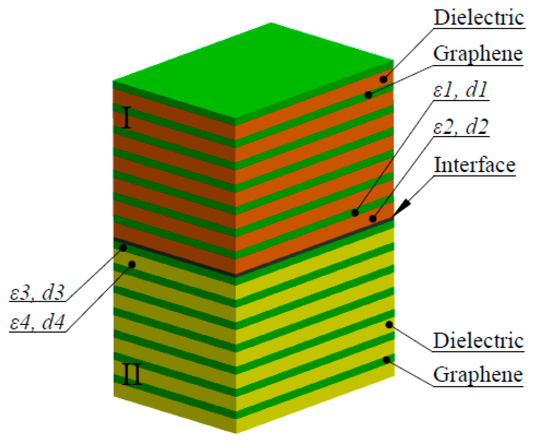
3. Two-Layered MMs for Surface Plasmon Polariton Guiding
Figure 2 is a schematic view of a hyperbolic multilayered MM consisting of periodically changing graphene and dielectric layers.
The effective-medium theory [
21] can be applied if the width of any sheet is much smaller than the wavelength of radiation. This approach allows us to describe the optical response in such a structure.
Herein, we present the dispersion branches calculated after carrying out the homogenization of two MMs. The dispersion pattern for the case
,
and
is presented in
Figure 3.
Figure 3 demonstrates that the SPPs branch at the interface separating MMs with
d1 = 0.35 nm,
d2 = 10 nm,
d3 = 0.25 nm, and
d4 = 10.1 nm. Moreover, the dispersion diagrams of SPPs, characterized by the effective properties outlined in [
21], are displayed in
Figure 3.
The tunability feature of the frequency ranges of SPPs is the main outcome of changing the Fermi energy. It is worthwhile noting that the decrease of the Fermi energy
μ causes movement of the dispersion diagrams to lower frequency ranges. On the contrary, the increase of the Fermi energy
μ will stimulate their movement to higher frequencies. As illustrated in
Figure 3, the smallest asymptotic frequency is achievable in the case of the smallest Fermi energy. The presented controllability feature provides possibilities to engineer the SPPs by the Fermi energy of the graphene layers. Consequently, special phase-matching tools, such as a grating or prism coupling [
22], near-field excitation [
23], and end-fire coupling [
24], are needed for their excitation via three-dimensional beams [
3].
Because of the graphene being treated as lossless,
β is complex resulting in a finite propagation length, presented in
Figure 3b.
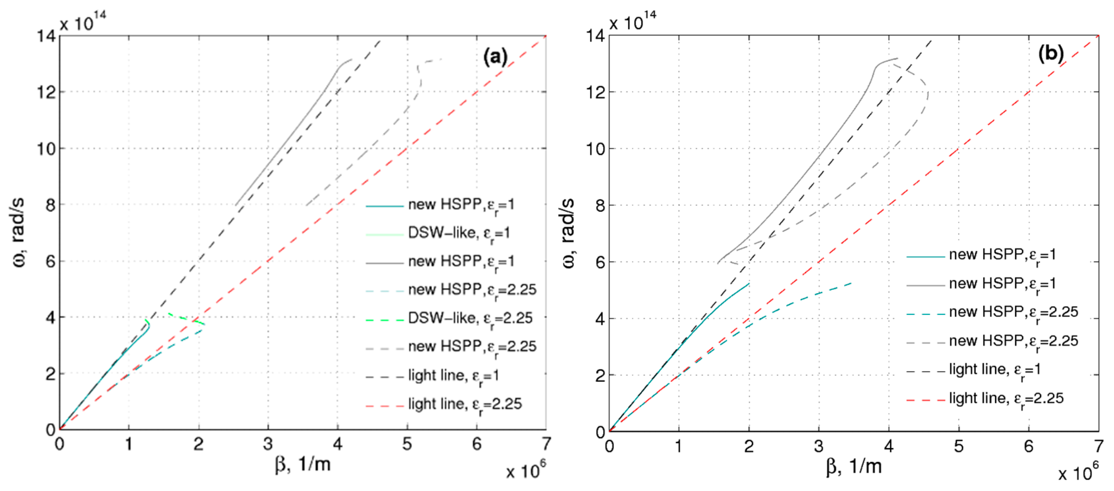
The next case to deal with, i.e.
,
and
, is studied by sketching four modes in
Figure 4 at the interface of the MMs with
ε4 = 2.25. As it follows from
Figure 4, the case
eV is characterized by the smallest asymptotic frequency. It is worthwhile noting, that
Re(
β) ≠ 0 allows for the quasi-bound [
21], leaky region of the dispersion equation.
Following the previous instances, the transverse magnetic (TM) mode dispersion plots are used to deal with the case of
,
and
,
. Four various modes are presented in
Figure 5. The outcome of tuning the fill ratios is examined as displayed in
Figure 5. Firstly, it is worth discussing how the dielectric thickness
dd impacts the dispersion branch (see
Figure 5a). It is found that an increase of
dd causes a shift of the upper limit to higher frequencies. Moreover, one can manipulate the frequency range for SPPs by tuning the number of graphene sheets, as shown in
Figure 5c.
It should be mentioned that, following [
25], it is of particular importance to omit negative values of the electrical length and absorption in
Figure 3b,c,
Figure 4b,c and
Figure 5b,d–f. The effect of absorption control was considered in [
26]. It was proposed to tune and enhance the absorption of thin dye-doped polymeric films by metallic and lamellar metal-dielectric hyperbolic metamaterial substrates. Herein, by employing graphene as a building block of the hyperbolic metamaterial, we achieve a higher level of tunability by changing the Fermi energy. Additionally, the sketched graphs represent clear evidence of the existing SPPs propagating for a long distance. The former is possible because the real part of
β is very low within this spectral range. It is of particular importance to mention that the same case appears when dealing with the boundary separating the MM and isotropic medium [
27].
The imaginary parts of the wavevector (i.e., absorption) are demonstrated in
Figure 3c,
Figure 4c and
Figure 5e,f. The absorption resonances allow for the rich phenomenon, i.e., behavior of the simple multilayered MMs as directive and monochromatic thermal sources [
28] without possessing any periodic corrugation.
We used a modal analysis to demonstrate that the bulk absorption in MMs arises because of the excitation of leaky bulk polaritons named FB modes [
29,
30,
31]. It is worthwhile noting that the interaction of the bulk plasmon with free space light at frequencies close to the metal epsilon-near-zero (ENZ) [
32] is possible. This method has been addressed by Ferrell for metallic foils in [
33], and by Berreman for polar dielectric films in [
34]. Radiative excitations called FB modes are possible due to the application of the multilayered MMs with graphene layers. It should be noted that these FB modes differ from SPPs, possibly due to the usage of metal foils. The former occurs because of energy propagating along the surfaces of the metal in cases of SPP modes. With respect to
Figure 3a and
Figure 4a,c, particular attention should be paid to FB modes existing at energies close to the ENZ of the hyperbolic MM to the left of the light line. A specific example of a three-layered MM and its dispersion engineering, allowing the development of new devices, are studied in detail in the next section.
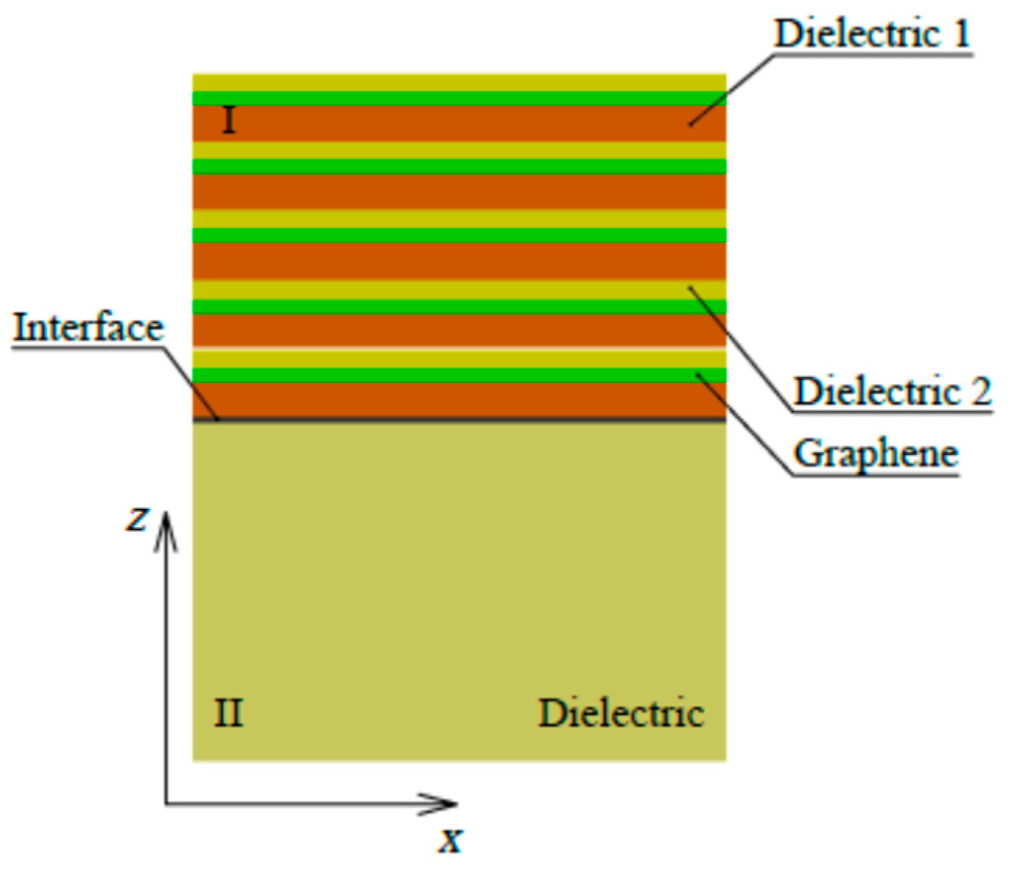
4. Three-Layered MMs for Surface Plasmon Polariton Guiding
Figure 6 illustrates a diagram of dielectric/graphene/dielectric multilayered MM.
It should be mentioned that the MM under study is described by effective permittivity tensor as follows:
in the principal-axis coordinate system. The principal values of the tensor are obtained in [
35,
36] by means of the theoretical approach provided in
Section 2:
where
and
,
represent the graphene and first dielectric filling ratios, respectively,
dg is the thickness of the graphene layer,
d1 is the thickness of the first dielectric sheet,
d2 is the thickness of the second dielectric layer,
ε1 is the permittivity of the first dielectric, and
ε2 is the permittivity of the second dielectric.
For the different cases presented in
Figure 7, dispersion relations are obtained as follows
In consequence, a surprising result is obtained: the thicknesses of the layers (
Figure 7c,d) do not affect the dispersion of a (single) boundary mode, and it agrees with the dispersion of a conventional SPP at a metal–dielectric boundary. It can be concluded that the systems displayed in
Figure 7c,d can support topological properties.
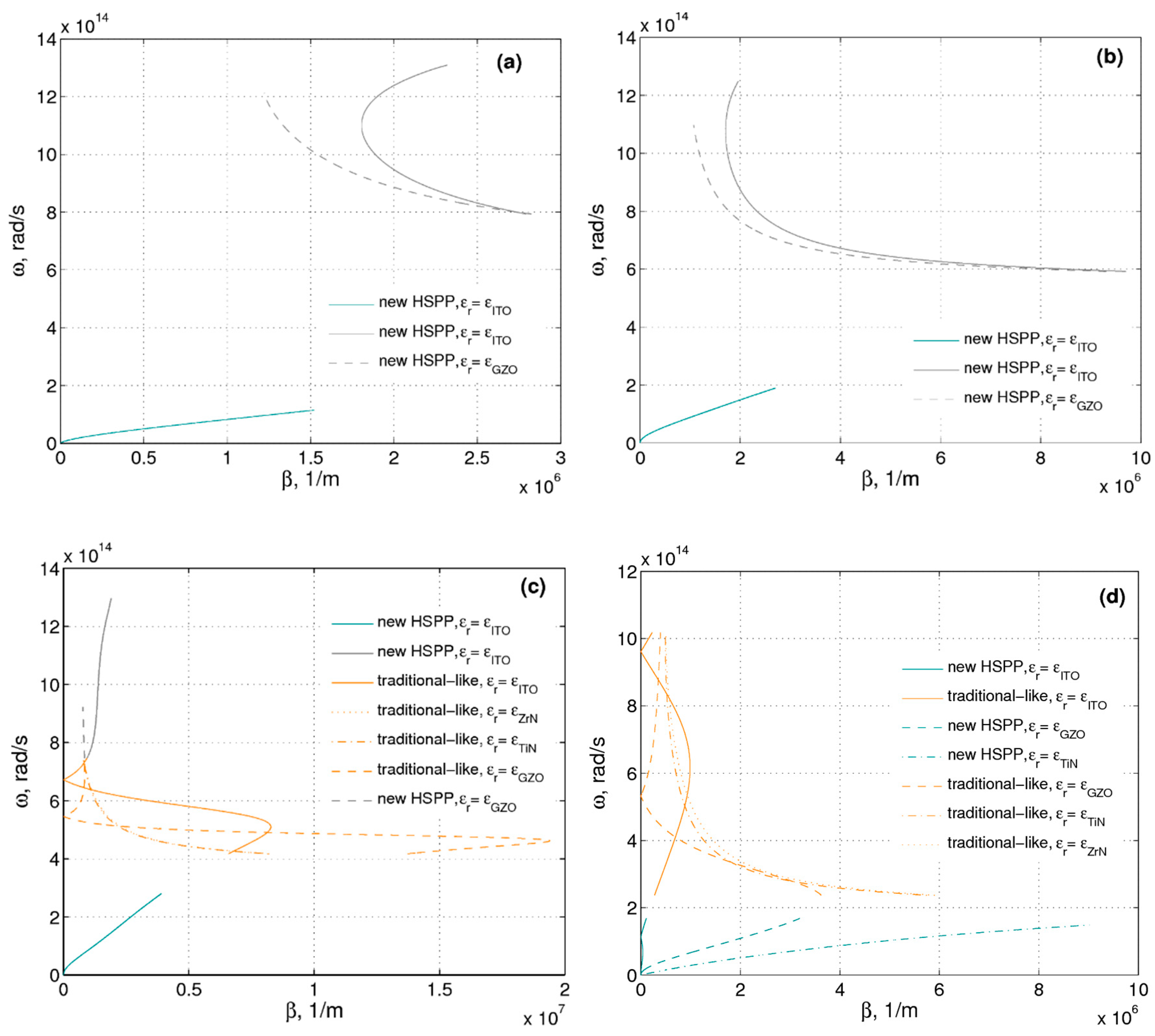
Herein, we present dispersion diagrams calculated after carrying out the homogenization of two MMs. Thus,
Figure 8 shows the dispersion branches of different cases of the multilayered MM. The dispersion branches of spoof SPPs at the MM interface with
dg = 0.35 nm are shown in
Figure 8. It should be noted that the case displayed in
Figure 8a (
ε1 = 18.8) corresponds to Equation (15). Thus, it can be concluded that the usage of the three-layered MM allows for the rich phenomenon, i.e., broadening of the frequency range of the SPP’s existence by approximately 800 THz. The dispersion curve computed for the three-layered MM case has special features deserving of attention, besides the fact that the graph resembles behavior of a traditional metal SPP and multilayered MMs [
21].
For SPPs supported by the multilayered MM under study, the horizontal asymptote appears when
β approaches infinity. Based on the dispersion equation [
21], the corresponding condition is as follows:
In other words, the position of horizontal asymptotes is determined by Equation (17). It is also concluded that must share the same sign with . It is worthwhile noting that will drastically affect the curve type.
Equation (17) holds only when both
and
are negative when
is larger than
. The former scenario matches band 2 in
Figure 9. Consequently, the dispersion branch possesses only one horizontal asymptote resembling the metal SPP case. The dispersion branch under such constraints bears a close resemblance to a metal and multilayered MM SPP [
21] (see
Figure 8).
Similar to ωsp for metal, the upper bound for SPP is marked by the location of the lowest horizontal asymptote. ωupper denotes the upper bound frequency, aiming to separate the upper bound of multilayered SPPs and that of metal SPPs (i.e., ωsp). One can easily prove that it is possible to excite multilayered SPPs at any frequency lower than ωupper in band 2.
The dispersion curve (
Figure 8) is obtained following the hypothesis of the EM field decaying exponentially in the
z direction. It should be noted that not all modes with a certain frequency below
ωupper is SPP in this study. The former takes place even though the dispersion curve displayed in
Figure 10 resembles the behavior of conventional metal SPP. One should be assured that both
and
are imaginary when aiming to obtain the multilayered SPPs. It can be concluded, based on
Figure 10, that the two cut-off points,
ωlower and
ωupper cut the frequency range into three regions. One may define
ωupper as the frequency of the lowest horizontal asymptote in the dispersion branch. It is worthwhile noting that
ωlower, which is lower than
ωupper, is the frequency where
and
are converted from real to imaginary.
The imaginary part of
in a multilayered MM is negligible, while the real part exists as indicated in
Figure 10, in region 1. The former proves the possibilities of the EM wave propagating into the material, resulting in a little damping. Region 1 is ended by frequency
ωlower. The same frequency begins region 2.
possesses a negligible real part and relatively large imaginary part in region 2. The former describes the evanescence of the field is in this region. The imaginary part of
disappears and the real part of
occurs if
ωupper is lower than the frequency (in region 3). The wavevector component
in the dielectric is shown in the right figure in
Figure 10. In the same way, the wave can propagate into the dielectric in areas 1 and 3, however, it is bounded to the boundary in area 2.
The SPPs can be controlled by tuning the Fermi energy. The former is in line with the dependence of
on the Fermi energy [
21]. It is worthwhile noting that the decreases in the Fermi energy
μ will cause a shift of the dispersion curves to higher wavelengths or lower frequencies. On the contrary, they will be shifted to higher frequencies because of the increases in the Fermi energy
μ. The smallest asymptotic frequency is attained in the case of the smallest Fermi energy, as indicated in
Figure 9. The former tunability property enables the SPP to be modified by the Fermi energy of the graphene layers.
Considering the next case, i.e.,
ε1 ≠ const, in
Figure 8a, three modes are represented at the interface of MM with
ε2 = 18.8. As displayed in
Figure 8a, the smallest asymptotic frequency matches the case
ε1 = 18.8. Also,
Re(
β) ≠ 0 allows for the presence of the quasi-bound [
37], leaky range of the dispersion equation. Consequently,
β does not approach infinity as the surface plasmon frequency is attained.
The dispersion curves of the TM modes are computed while aiming to address the case
fg ≠ const and
f1 ≠ const. In
Figure 8c,d, eight different branches are presented. One should consider the impact of the fill ratios of the dielectric and graphene layer, as sketched in
Figure 8c,d. First, the impact of the width of the graphene
fg on the dispersion branch (see
Figure 8c) should be discussed. It is found that the decrease of
fg causes a shift of the upper limit to higher frequencies. Additionally, one can control the frequency range of SPPs by changing the dielectric filling ratio, as demonstrated in
Figure 8d.
We will address the tunable hyperbolic MM made of TCO-dielectric multilayered MMs in the next section, aiming to obtain a new type of SPP.
5. Tunable Hyperbolic MM Made of TCO-Dielectric Multilayered MMs
The proposed MM is displayed in
Figure 11. Herein,
dTCO and
dd are the widths of the TCO and dielectric sheets, correspondingly. A TCO/PbS MM is considered, aiming to study the dispersive properties of SPPs. It is assumed that
εd = 18.8 for PbS sheets, and
εTCO is computed by means of the parameters outlined in [
38].
For the instance of the anisotropic material, the EM wave dispersions can be sketched for MM/dielectric and the MM/TCO instances. Let us concentrate on a semi-infinite AZO (Aluminum Zinc Oxide)/PbS MM example while tackling the numerical calculations. Moreover, a homogenization of the MM matching the MM/dielectric and MM/TCO boundaries is considered. Sketching the branches of the permittivities (
and
) and the dielectric constant (
) allows us to consider the optical properties. Moreover, we consider different frequency ranges, distinguishing them based on the properties of and relation among
,
, and
[
39].
- (1)
and (cyan);
- (2)
(green);
- (3)
and (gray);
- (4)
and (magenta) and
- (5)
(orange).
It is worthwhile mentioning that the effective parameters will dramatically influence the SPPs, as outlined in [
39]. The TCO filling ratio,
fTCO, is used here as the main mechanism controlling the effective optical parameters.
Figure 12 and
Figure 13 display characteristic dispersion branches, considering different TCO filling factors. Different branch colors are applied, aiming to distinguish various frequency ranges. One can distinguish three SPPs fitting three different ranges in the case of
fTCO = 0.3 and MM/dielectric boundary. Moreover, two kinds of SPPs are observed in the instance of the MM/TCO boundary. For the MM/TCO case, the upper waves are in the gray region. The
fTCO = 0.5, 0.7, 0.9 cases are associated with three exceptional cases. In the case of
fTCO = 0.5, two types of SPPs appear in two color ranges, i.e., cyan and gray for the MM/dielectric and MM/TCO boundaries. The upper short branches in the case of
fTCO = 0.7, lying in the gray range, are presented in
Figure 12 and
Figure 13. The other SPPs belong to the orange range. The supplementary SSPs belonging to the magenta range are observed with respect to a MM/dielectric boundary. A dark-magenta color displays an extension approach for the magenta region in the case of
. One may observe two kinds of SPPs belonging to the orange and cyan ranges for the MM/TCO instance and three types of SPPs lying in the cyan, orange, and gray ranges for the MM/dielectric case with a filling factor
fTCO = 0.9. It should be underlined that one SPP occurs in the cyan range for different TCO filling factors in the MM/dielectric case. The former is outlined in
Figure 12. It is of importance that the case
opens the gateway for possible applications, as the SPP always occurs in the cyan range for different filling factors (
Figure 13).
Following the essential condition for the presence of the Dyakonov-like SPP (DSW) [
35], the SPP in the green resembles the behavior of a DSW. Thus, it is important to address DSW [
40], or the Dyakonov defined in [
35]. Furthermore, the frequency region of the DSW can be extended by using the
material at the right-hand side of the boundary (
Figure 12). The dark-green color [
39] is applied, seeking to outline the former extension. Particularly, the extension of the gray region [
39] is probable because of the usage of ITO (Indium Tin Oxide) instead of GZO (ZnO:Ga) at the right-hand side of the boundary [
39]. The SPP in the orange range is similar to the traditional SPP. The former happens because of the negative principal values of the effective permittivity in the orange range. Thus, this SPP should be associated with an SPP of a traditional type. The others are novel kinds of SPPs. Therefore, all the SPPs belong to the five different types, located in the five color ranges in
Figure 12, correspondingly. In the instance of the AZO/PbS MM and air/dielectric boundary, five types of SPPs appear, and only three are found for the AZO/PbS MM and TCO interface.
Unavoidably, a traditional-like SPP is characterized by an ordinary dispersion for the MM/dielectric boundary, occurring to the right of the light line. Altogether, the degradation of the dispersion in the orange range might be observed in the instance of the MM/TCO boundary. One can manipulate the dispersion features controlling the TCO filling factor in the MM realization. It should be noted that for a low TCO filling factor, in the case of the MM/TCO boundary, two kinds of the modes always exist, while for higher TCO filling factors, modes in the gray range disappear (
Figure 13d).
It should be mentioned that the complex mode diagrams (
Figure 12 and
Figure 13), which match either the MM/dielectric or MM/TCO boundary, appear due to the confinement of SPPs in the direction perpendicular to the wave propagation. The origin of these EM SPPs is caused by the coupling of the EM fields to the oscillations of the conductor’s electron plasma.
6. Conclusions
6.1. Two-Layered MMs for Surface Plasmon Polariton Guiding
To conclude, we have presented a research approach to describe the dispersion of hyperbolic MMs. The aim of these studies is to mitigate the problem under consideration, offering tuning possibilities of the hyperbolic features. The former is tremendously needed from the perspective of device applications. In this regard, we presented a multilayered MM. In the light of the present work, we have outlined the tunable features of the effective permittivity of the graphene-based MMs. Three significant outcomes should be outlined, in view of the obtained results. Firstly, compared with the dispersion equation in the instance of , , and , the quasibound, leaky part of the dispersion equation is narrowed for the case , and . Secondly, one may control the perpendicular component of effective permittivity by manipulating the Fermi energy, the width of dielectric, and the number of graphene sheets in the MMs. Thirdly, one can engineer the frequency range of the SPP by changing the Fermi energy of graphene and the fill ratio of the dielectric or graphene layers in the unit cell of the MMs.
6.2. Tunable Hyperbolic MM Made of TCO-Dielectric Multilayered MMs
SPPs in a TCO-dielectric MM have been studied. Like graphene-dielectric MM [
21], a TCO-dielectric MM support traditional-like SPPs possessing various diagrams matching two various boundaries. Based on theoretical considerations [
40], the dispersion equations of SPPs were obtained. Five types of SPPs, among which three types are novel SPP types, one is DSW, and another is the traditional-like SPP, are foreseen. The existence of these SPPs is impacted by the features of the principal values of the effective permittivity. It should be noted that the presented (new) types of SPPs appear due to the principal values of the effective pemittivity being functions of frequency. Additionally, SPPs with a dispersion coinciding with the dispersion of a surface plasmon at the interface of two isotropic media are foreseen to match the MM boundary if the material at the right-hand side is the same as that used in the MM.
6.3. Three-Layered MMs for Surface Plasmon Polariton Guiding
SPP supported by graphene/dielectric multilayered MMs was studied theoretically. It is concluded that SPP can be supported by a three-layered MM. Also, one can easily manipulate the characteristics of the multilayered SPPs by manipulating the structural parameters. Thus, the active materials can be included into the MM design, which might open wide avenues for future devices.
The dielectric permittivity should be smaller than the absolute value of
Re(
εm), aiming to fulfill the EM boundary condition and statements of continuity [
41] in the case of a traditional metal SPP. If not, the SPP mode would be cut off. The property of anisotropic material is represented by multilayered MMs if the case is considered from the effective medium perspective. Further, it is shown in
Figure 9 that one may deal with multilayered MMs as with anisotropic metal near the upper bound of its SPP frequency region (in band 2). The
is far from zero, while
is much closer to zero within band 2 of
Figure 9, compared with
Re(
εm) of pure metal.
The effective permittivity is caused by the interaction of the EM field with the free electrons in graphene sheets and the SPP mode coupling and resonance in multilayered MM. Consequently, the SPP frequency region is extended due to the SPP mode coupling and resonance in the multilayered MMs, characterized by anisotropic permittivity.
It is worthwhile noting that the multilayered SPPs could also be excited by means of the evanescent EM field generated by a prism or waveguide. Extended frequency range, lower propagation loss, and controllable features are possible due to the changes of the graphene/dielectric ratio, and these properties might open a gateway for possible applications in biosensor and active SPP devices.
Herein, we have theoretically considered the SPP guided by dielectric/graphene/dielectric multilayered MMs. One may conclude that an SPP can propagate when the MM is at the frequency where a conventional metal SPP cannot occur, as in the case of high permittivity of dielectric on metal. In addition to the variance of a high frequency cut-off point in comparison with metal SPPs, it was observed that a low cut-off frequency, below which SPP could not be supported by the MM, exists.
These outstanding properties open wide avenues for the usage of an SPP mode for some potential applications, which are impossible for metal SPPs. In addition to the characteristics of the multilayered SPPs being easily controlled by tuning the composite parameters, the active materials can also be incorporated into the MM. This described feature might also create new possibilities for future devices.


