Grating-Assisted Fiber to Chip Coupling for SOI Photonic Circuits


Abstract
1. Introduction
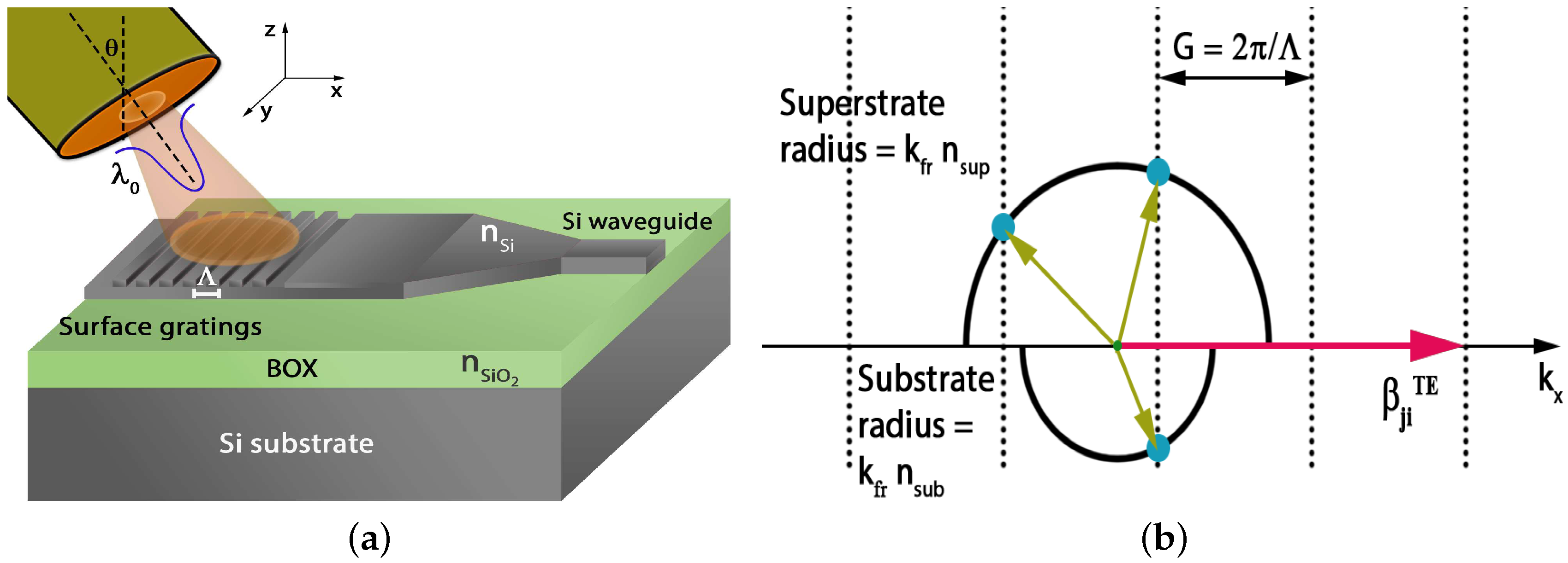
2. Coupling through Gratings: Theory and Fundamentals
3. Factors Affecting Grating Loss
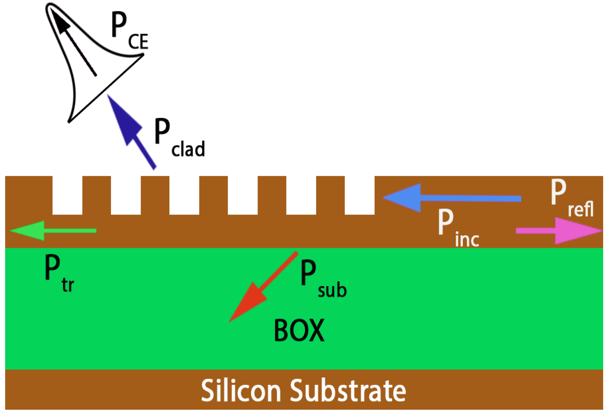
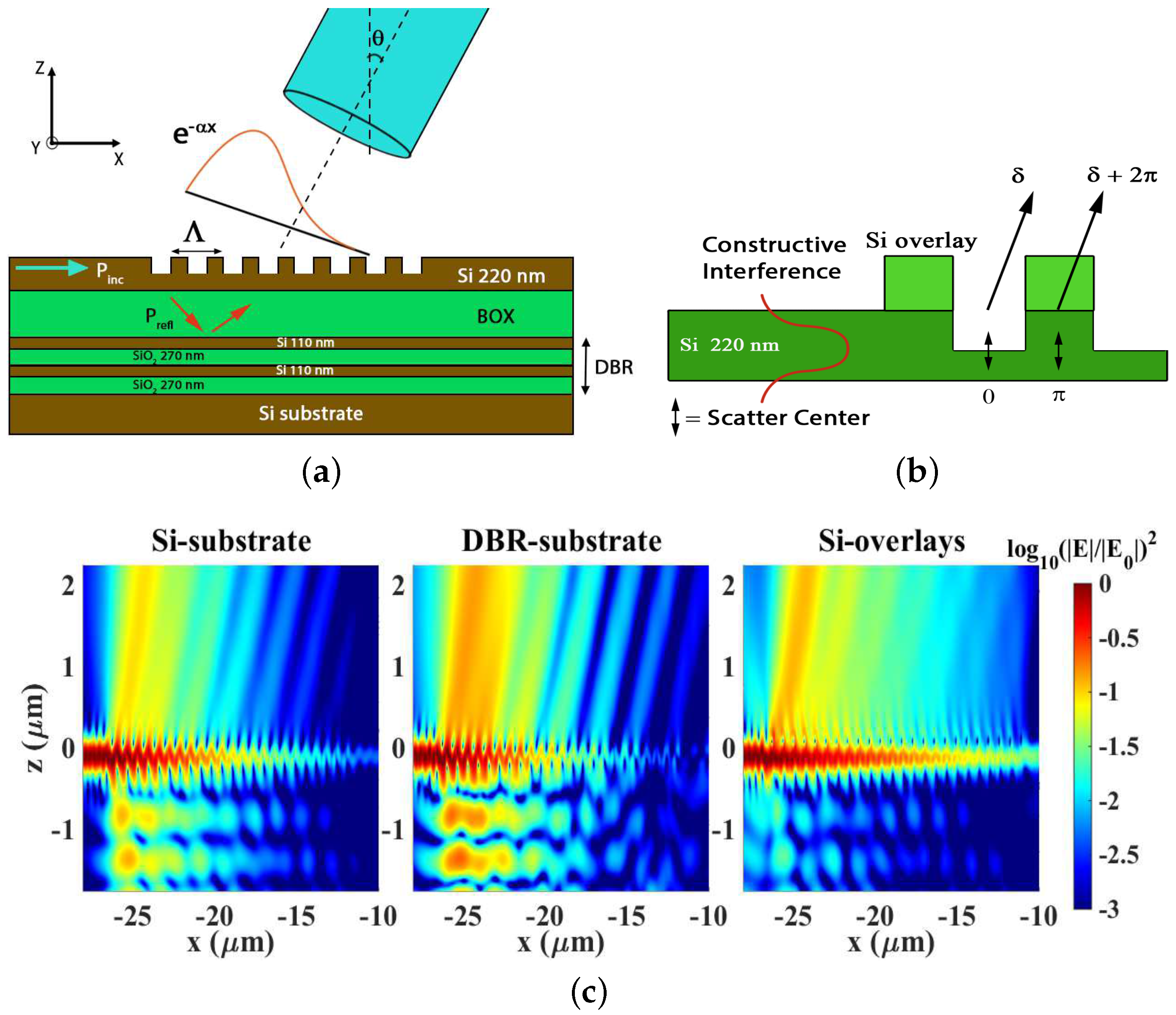
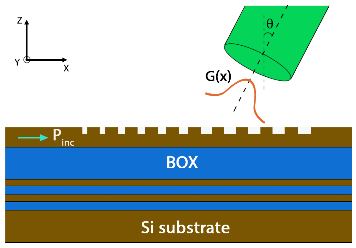
3.1. Directionality
3.2. Mode Overlap
3.3. Bandwidth Scaling
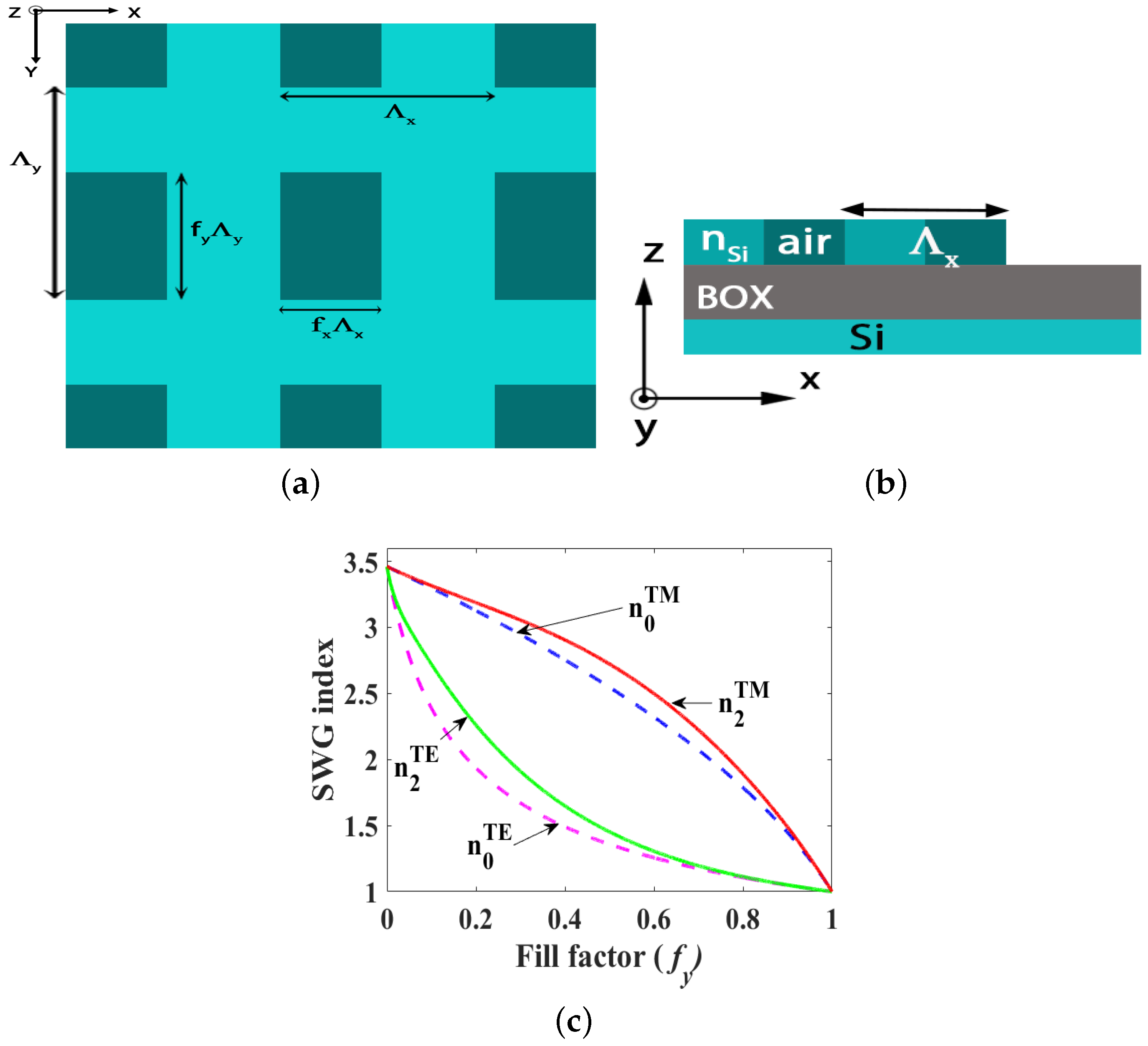
4. Subwavelength Gratings
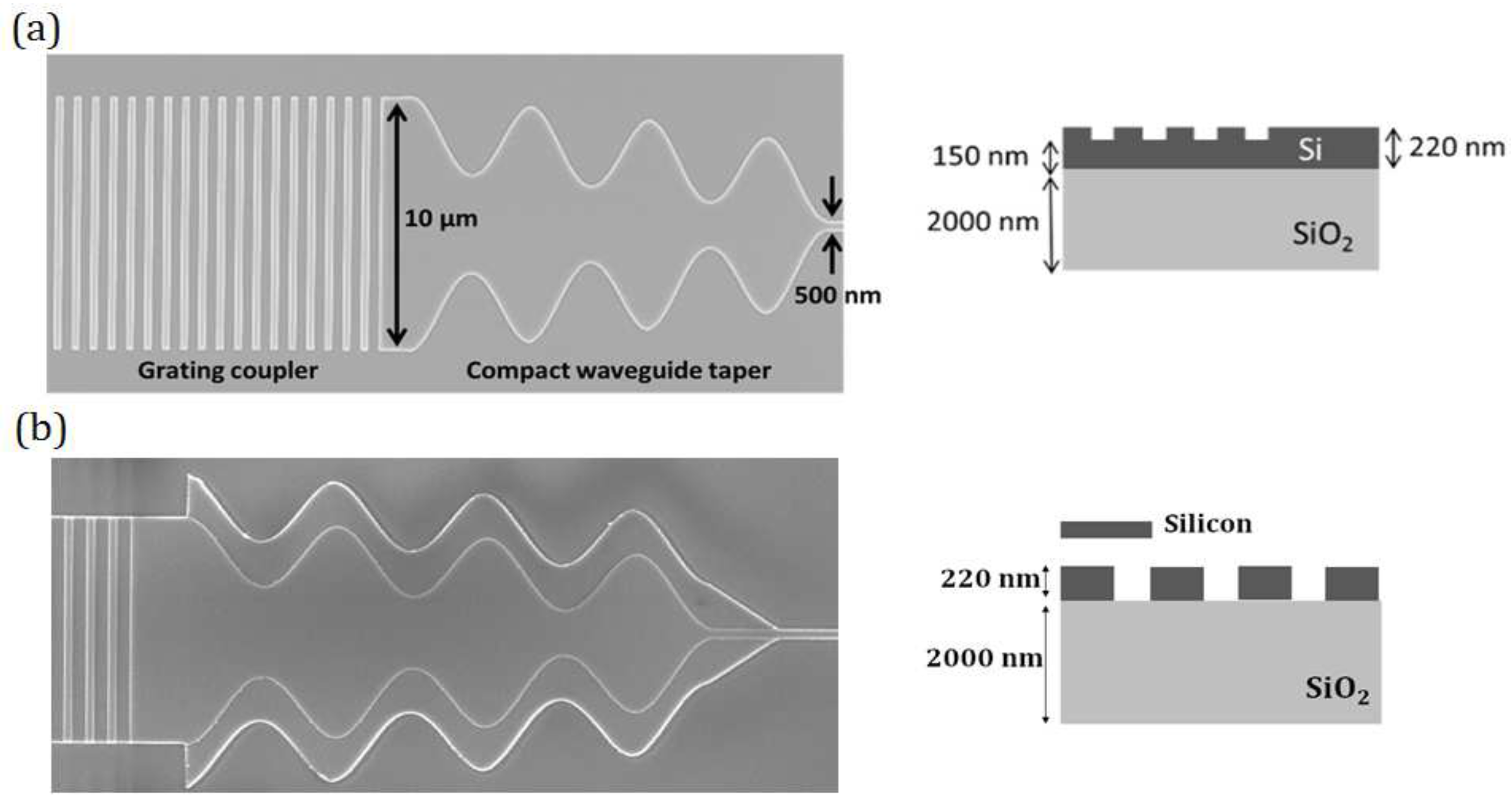
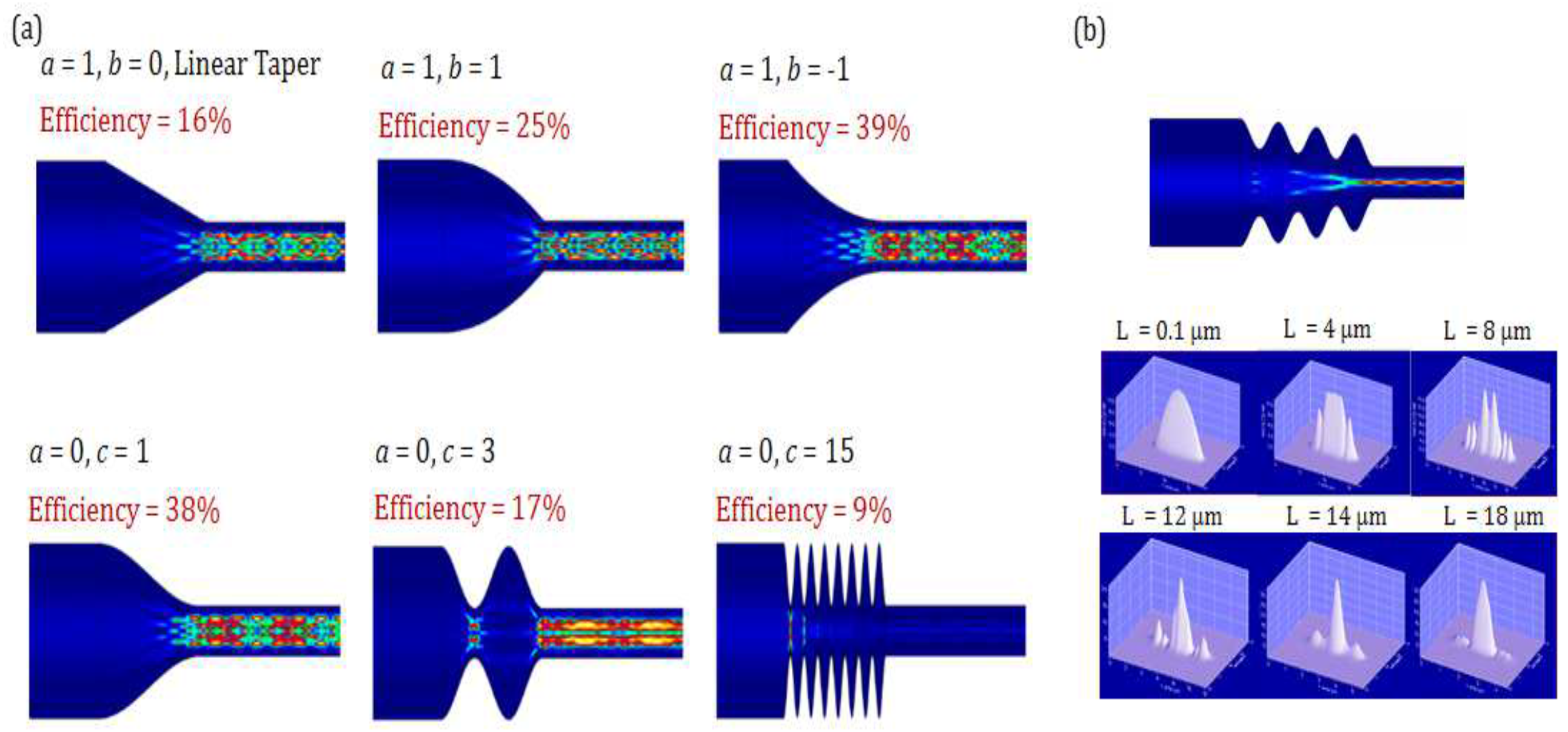
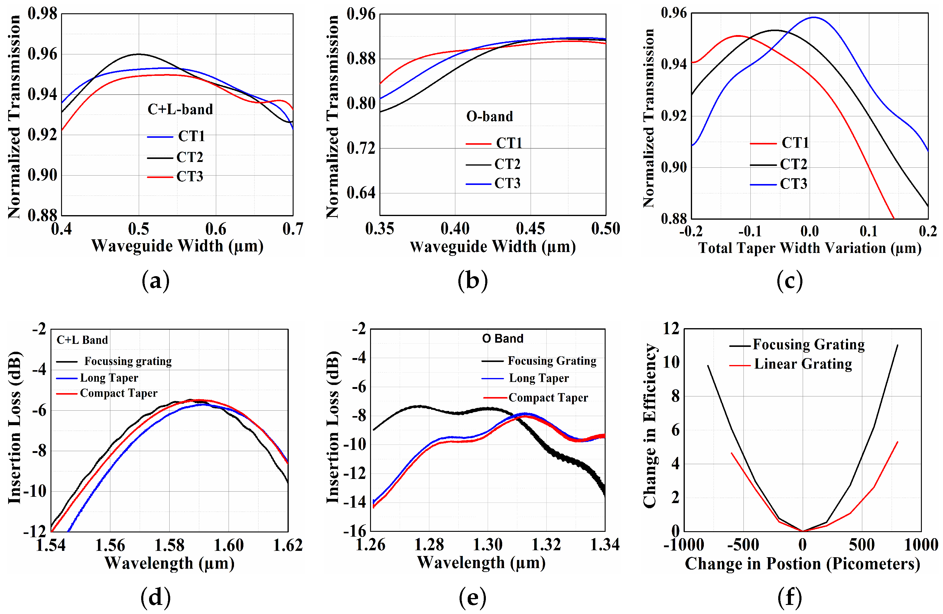
5. Lowering Footprint
5.1. Focusing Gratings
5.2. Linear Grating Based Compact Tapers
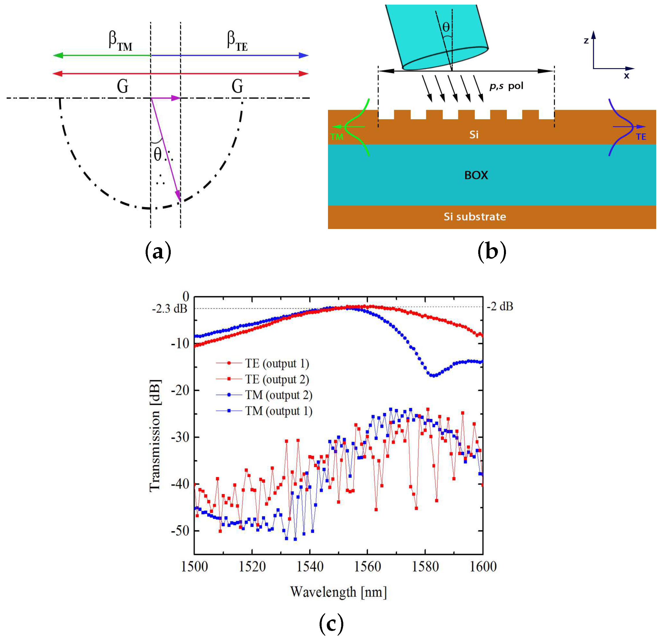
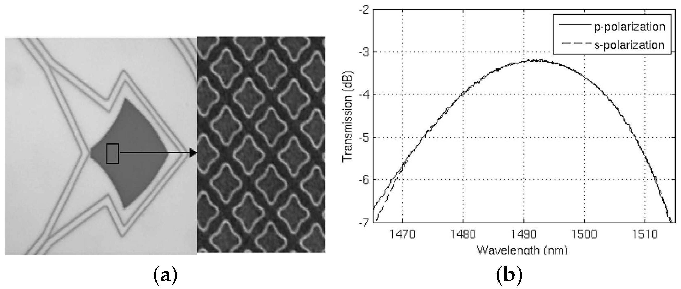
6. Polarization Splitting Grating Couplers (PSGC)
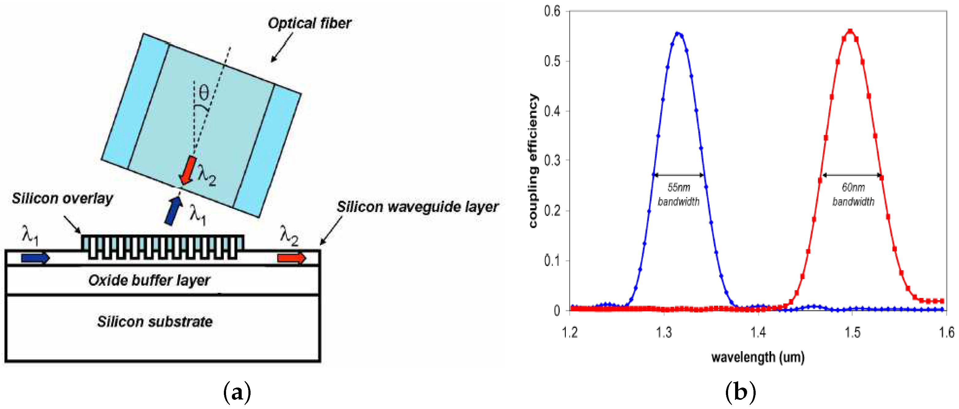
7. Dual Band Grating Couplers
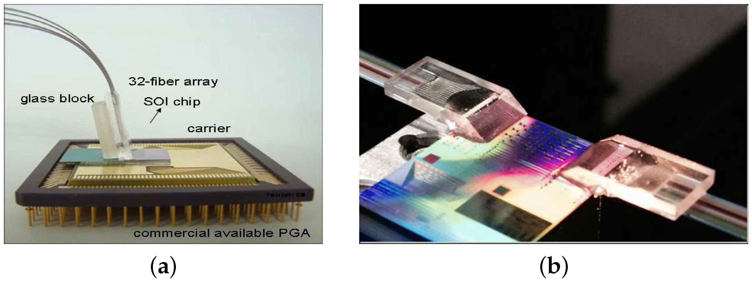
8. Packaging and Testing
9. Conclusions
Author Contributions
Funding
Acknowledgments
Conflicts of Interest
Abbreviations
| SOI | Silicon-on-Insulator |
| DBR | distributed Bragg reflector |
| PSGC | polarization splitting grating coupler |
| PDL | polarization dependent loss |
| TE | transverse electric |
| TM | transverse magnetic |
| SWG | subwavelength grating |
References
- Atabaki, A.H.; Moazeni, S.; Pavanello, F.; Gevorgyan, H.; Notaros, J.; Alloatti, L.; Wade, M.T.; Sun, C.; Kruger, S.A.; Meng, H.; et al. Integrating photonics with silicon nanoelectronics for the next generation of systems on a chip. Nature 2018, 556, 349. [Google Scholar] [CrossRef] [PubMed]
- Absil, P.P.; Verheyen, P.; De Heyn, P.; Pantouvaki, M.; Lepage, G.; De Coster, J.; Van Campenhout, J. Silicon photonics integrated circuits: A manufacturing platform for high density, low power optical I/O’s. Opt. Express 2015, 23, 9369. [Google Scholar] [CrossRef] [PubMed]
- Shankar Kumar, M.G.; Milenin, A.; Delvaux, C.; Ong, P.; Pathak, S.; Vermeulen, D.; Sterckx, G.; Winroth, G.; Verheyen, P.; Lepage, G.; et al. Advanced 300-mm waferscale patterning for silicon photonics devices with record low loss and phase errors. In Proceedings of the 17th Opto-Electronics and Communications Conference (OECC-2012), Busan, Korea, 2–6 July 2012; pp. 15–16. [Google Scholar]
- Wang, J.; Paesani, S.; Ding, Y.; Santagati, R.; Skrzypczyk, P.; Salavrakos, A.; Tura, J.; Augusiak, R.; Mančinska, L.; Bacco, D.; et al. Multidimensional quantum entanglement with large-scale integrated optics. Science 2018, 360, 285–291. [Google Scholar] [CrossRef] [PubMed]
- Alloatti, L.; Palmer, R.; Diebold, S.; Pahl, K.P.; Chen, B.; Dinu, R.; Fournier, M.; Fedeli, J.M.; Zwick, T.; Freude, W.; et al. 100 GHz silicon–organic hybrid modulator. Light Sci. Appl. 2014, 3, e173. [Google Scholar] [CrossRef]
- Almeida, V.R.; Panepucci, R.R.; Lipson, M. Nanotaper for compact mode conversion. Opt. Lett. 2003, 28, 1302–1304. [Google Scholar] [CrossRef] [PubMed]
- Bakir, B.B.; de Gyves, A.V.; Orobtchouk, R.; Lyan, P.; Porzier, C.; Roman, A.; Fedeli, J.M. Low-Loss (<1 dB) and Polarization-Insensitive Edge Fiber Couplers Fabricated on 200-mm Silicon-on-Insulator Wafers. IEEE Photonics Technol. Lett. 2010, 22, 739–741. [Google Scholar]
- Pu, M.; Liu, L.; Ou, H.; Yvind, K.; Hvam, J.M. Ultra-low-loss inverted taper coupler for silicon-on-insulator ridge waveguide. Opt. Commun. 2010, 283, 3678–3682. [Google Scholar] [CrossRef]
- Yariv, A.; Yeh, P. Photonics: Optical Electronics in Modern Communications (The Oxford Series in Electrical and Computer Engineering); Oxford University Press, Inc.: New York, NY, USA, 2006. [Google Scholar]
- Kopp, C.; Augendre, E.; Orobtchouk, R.; Lemonnier, O.; Fedeli, J.M. Enhanced fiber grating coupler integrated by wafer-to-wafer bonding. J. Light. Technol. 2011, 29, 1847–1851. [Google Scholar] [CrossRef]
- Selvaraja, S.K.; Vermeulen, D.; Schaekers, M.; Sleeckx, E.; Bogaerts, W.; Roelkens, G.; Dumon, P.; Thourhout, D.V.; Baets, R. Highly efficient grating coupler between optical fiber and silicon photonic circuit. In Proceedings of the 2009 European Conference on Lasers and Electro-Optics, Munich, Germany, 14–19 June 2009; pp. 1–2. [Google Scholar]
- Siddharth, R.; Nambiar, S.K.S. High-efficiency broad-bandwidth subwavelength grating-based fiber-chip coupler in silicon-on-insulator. Opt. Eng. 2018, 57, 017115. [Google Scholar]
- Zaoui, W.S.; Kunze, A.; Vogel, W.; Berroth, M.; Butschke, J.; Letzkus, F.; Burghartz, J. Bridging the gap between optical fibers and silicon photonic integrated circuits. Opt. Express 2014, 22, 1277–1286. [Google Scholar] [CrossRef] [PubMed]
- Zaoui, W.S.; Rosa, M.F.; Vogel, W.; Berroth, M.; Butschke, J.; Letzkus, F. Cost-effective CMOS-compatible grating couplers with backside metal mirror and 69% coupling efficiency. Opt. Express 2012, 20, B238–B243. [Google Scholar] [CrossRef] [PubMed]
- Vermeulen, D.; Selvaraja, S.; Verheyen, P.; Lepage, G.; Bogaerts, W.; Absil, P.; Van Thourhout, D.; Roelkens, G. High-efficiency fiber-to-chip grating couplers realized using an advanced CMOS-compatible Silicon-On-Insulator platform. Opt. Express 2010, 18, 18278–18283. [Google Scholar] [CrossRef] [PubMed]
- Taillaert, D.; Bienstman, P.; Baets, R. Compact efficient broadband grating coupler for silicon-on-insulator waveguides. Opt. Lett. 2004, 29, 2749–2751. [Google Scholar] [CrossRef] [PubMed]
- Tang, Y.; Wang, Z.; Wosinski, L.; Westergren, U.; He, S. Highly efficient nonuniform grating coupler for silicon-on-insulator nanophotonic circuits. Opt. Lett. 2010, 35, 1290–1292. [Google Scholar] [CrossRef] [PubMed]
- Chen, X.; Li, C.; Fung, C.K.Y.; Lo, S.M.G.; Tsang, H.K. Apodized Waveguide Grating Couplers for Efficient Coupling to Optical Fibers. IEEE Photonics Technol. Lett. 2010, 22, 1156–1158. [Google Scholar] [CrossRef]
- Benedikovic, D.; Cheben, P.; Schmid, J.H.; Xu, D.X.; Lapointe, J.; Wang, S.; Halir, R.; Ortega-Moñux, A.; Janz, S.; Dado, M. High-efficiency single etch step apodized surface grating coupler using subwavelength structure. Laser Photonics Rev. 2014, 8, L93–L97. [Google Scholar] [CrossRef]
- Chen, X.; Xu, K.; Cheng, Z.; Fung, C.K.Y.; Tsang, H.K. Wideband subwavelength gratings for coupling between silicon-on-insulator waveguides and optical fibers. Opt. Lett. 2012, 37, 3483–3485. [Google Scholar] [CrossRef] [PubMed]
- Halir, R.; Ortega-Moñux, A.; Schmid, J.H.; Alonso-Ramos, C.; Lapointe, J.; Xu, D.X.; Wangüemert-Pérez, J.G.; Molina-Fernández, Í.; Janz, S. Recent Advances in Silicon Waveguide Devices Using Sub-Wavelength Gratings. IEEE J. Sel. Top. Quantum Electron. 2014, 20, 279–291. [Google Scholar] [CrossRef]
- Halir, R.; Bock, P.J.; Cheben, P.; Ortega-Moñux, A.; Alonso-Ramos, C.; Schmid, J.H.; Lapointe, J.; Xu, D.X.; Wangüemert-Pérez, J.G.; Molina-Fernández, Í.; Janz, S. Waveguide sub-wavelength structures: A review of principles and applications. Laser Photonics Rev. 2015, 9, 25–49. [Google Scholar] [CrossRef]
- Donzella, V.; Sherwali, A.; Flueckiger, J.; Grist, S.M.; Fard, S.T.; Chrostowski, L. Design and fabrication of SOI micro-ring resonators based on sub-wavelength grating waveguides. Opt. Express 2015, 23, 4791–4803. [Google Scholar] [CrossRef] [PubMed]
- Raguin, D.H.; Morris, G.M. Antireflection structured surfaces for the infrared spectral region. Appl. Opt. 1993, 32, 1154–1167. [Google Scholar] [CrossRef] [PubMed]
- Ding, Y.; Peucheret, C.; Ou, H.; Yvind, K. Fully etched apodized grating coupler on the SOI platform with -0.58 dB coupling efficiency. Opt. Lett. 2014, 39, 5348–5350. [Google Scholar] [CrossRef] [PubMed]
- Na, N.; Frish, H.; Hsieh, I.W.; Harel, O.; George, R.; Barkai, A.; Rong, H. Efficient broadband silicon-on-insulator grating coupler with low backreflection. Opt. Lett. 2011, 36, 2101–2103. [Google Scholar] [CrossRef] [PubMed]
- Shi, R.; Guan, H.; Novack, A.; Streshinsky, M.; Lim, A.E.J.; Lo, G.Q.; Baehr-Jones, T.; Hochberg, M. High-efficiency grating couplers near 1310 nm fabricated by 248-nm DUV lithography. IEEE Photonics Technol. Lett. 2014, 26, 1569–1572. [Google Scholar]
- Chen, X.; Thomson, D.J.; Crudginton, L.; Khokhar, A.Z.; Reed, G.T. Dual-etch apodised grating couplers for efficient fibre-chip coupling near 1310 nm wavelength. Opt. Express 2017, 25, 17864–17871. [Google Scholar] [CrossRef] [PubMed]
- Zhang, C.; Sun, J.H.; Xiao, X.; Sun, W.M.; Zhang, X.J.; Chu, T.; Yu, J.Z.; Yu, Y.D. High efficiency grating coupler for coupling between single-mode fiber and soi waveguides. Chin. Phys. Lett. 2013, 30, 8–12. [Google Scholar] [CrossRef]
- Benedikovic, D.; Alonso-Ramos, C.; Cheben, P.; Schmid, J.H.; Wang, S.; Halir, R.; Ortega-Moñux, A.; Xu, D.X.; Vivien, L.; Lapointe, J.; et al. Single-etch subwavelength engineered fiber-chip grating couplers for 1.3 μm datacom wavelength band. Opt. Express 2016, 24, 12893–12904. [Google Scholar] [CrossRef] [PubMed]
- Wang, Y.; Yun, H.; Lu, Z.; Bojko, R.; Shi, W.; Wang, X.; Flueckiger, J.; Zhang, F.; Caverley, M.; Jaeger, N.A.; et al. Apodized focusing fully etched subwavelength grating couplers. IEEE Photonics J. 2015, 7, 1–10. [Google Scholar] [CrossRef]
- Waldhäusl, R.; Schnabel, B.; Dannberg, P.; Kley, E.B.; Bräuer, A.; Karthe, W. Efficient Coupling into Polymer Waveguides by Gratings. Appl. Opt. 1997, 36, 9383–9390. [Google Scholar] [CrossRef] [PubMed]
- Sun, C.; Wade, M.T.; Lee, Y.; Orcutt, J.S.; Alloatti, L.; Georgas, M.S.; Waterman, A.S.; Shainline, J.M.; Avizienis, R.R.; Lin, S.; et al. Single-chip microprocessor that communicates directly using light. Nature 2015, 528, 534–538. [Google Scholar] [CrossRef] [PubMed]
- Pérez, D.; Gasulla, I.; Crudgington, L.; Thomson, D.J.; Khokhar, A.Z.; Li, K.; Cao, W.; Mashanovich, G.Z.; Capmany, J. Multipurpose silicon photonics signal processor core. Nat. Commun. 2017, 8, 636. [Google Scholar] [CrossRef] [PubMed]
- Moss, D.J.; Morandotti, R.; Gaeta, A.L.; Lipson, M. New CMOS-compatible platforms based on silicon nitride and Hydex for nonlinear optics. Nat. Photonics 2013, 7, 597–607. [Google Scholar] [CrossRef]
- Manolatou, C.; Haus, H. Compact mode-size converters for efficient coupling between fibers and integrated optical waveguides. In Proceedings of the 2001 Digest of LEOS Summer Topical Meetings: Advanced Semiconductor Lasers and Applications/Ultraviolet and Blue Lasers and Their Applications/Ultralong Haul DWDM Transmission and Networking/WDM Compo, Copper Mountain, CO, USA, 30 July–1 August 2001; Volume 3, p. 2. [Google Scholar]
- Shoji, T.; Tsuchizawa, T.; Watanabe, K.Y.; Morita, H. Low loss mode size converter from 0.3pm square Si wire waveguides to singlemode fibres. Electron. Lett. 2002, 38, 1669–1670. [Google Scholar] [CrossRef]
- Cheben, P.; Bock, P.J.; Schmid, J.H.; Lapointe, J.; Janz, S.; Xu, D.X.; Densmore, A.; Delâge, A.; Lamontagne, B.; Hall, T.J. Refractive index engineering with subwavelength gratings for efficient microphotonic couplers and planar waveguide multiplexers. Opt. Lett. 2010, 35, 2526–2528. [Google Scholar] [CrossRef] [PubMed]
- Van Laere, F.; Roelkens, G.; Ayre, M.; Schrauwen, J.; Taillaert, D.; Van Thourhout, D.; Krauss, T.F.; Baets, R. Compact and highly efficient grating couplers between optical fiber and nanophotonic waveguides. J. Light. Technol. 2007, 25, 151–156. [Google Scholar] [CrossRef]
- Wu, J.; Shi, B.; Kong, M. Exponentially Tapered Multi-Mode Interference Couplers. Chin. Opt. Lett. 2006, 4, 167–169. [Google Scholar]
- Ye, T.; Fu, Y.; Qiao, L.; Chu, T. Low-crosstalk Si arrayed waveguide grating with parabolic tapers. Opt. Express 2014, 22, 31899–31906. [Google Scholar] [CrossRef] [PubMed]
- Fu, Y.; Ye, T.; Tang, W.; Chu, T. Efficient adiabatic silicon-on-insulator waveguide taper. Photonics Res. 2014, 2, A41. [Google Scholar] [CrossRef]
- Luyssaert, B. A versatile spot-size converter design. In Proceedings of the Proceedings Symposium IEEE/LEOS Benelux Chapter, Ghent, Belgium, 2–3 December 2004; pp. 2–5. [Google Scholar]
- Van Acoleyen, K.; Baets, R. Compact lens-assisted focusing tapers fabricated on silicon-on-insulator. In Proceedings of the 8th IEEE International Conference on Group IV Photonics, London, UK, 14–16 September 2011; pp. 157–159. [Google Scholar]
- Vermeulen, D.; Van Acoleyen, K.; Ghosh, S. Efficient tapering to the fundamental quasi-TM mode in asymmetrical waveguides. In Proceedings of the 15th European Conference on Integrated Optics (ECIO 2010), Cambridge, UK, 7–9 April 2010; pp. 2–3. [Google Scholar]
- Sethi, P.; Haldar, A.; Selvaraja, S.K. Compact tapers for silicon grating fibre-chip couplers in O, C and L band. In Proceedings of the 2017 Conference on Lasers and Electro-Optics Europe European Quantum Electronics Conference (CLEO/Europe-EQEC), Munich, Germany, 25–29 June 2017; p. 1. [Google Scholar]
- Sethi, P.; Haldar, A.; Selvaraja, S.K. Ultra-compact low-loss broadband waveguide taper in silicon-on-insulator. Opt. Express 2017, 25, 10196–10203. [Google Scholar] [CrossRef]
- Sethi, P.; Haldar, A.; Selvaraja, S.K.; Kallega, R. Compact broadband taper for low-loss coupling to a silicon nitride photonic wire. In Integrated Optics: Devices, Materials, and Technologies XXII; International Society for Optics and Photonics: Washington, DC, USA, 2018; p. 75. [Google Scholar]
- Tang, Y.; Dai, D.; He, S. Proposal for a grating waveguide serving as both a polarization splitter and an efficient coupler for silicon-on-insulator nanophotonic circuits. IEEE Photonics Technol. Lett. 2009, 21, 242–244. [Google Scholar] [CrossRef]
- Zaoui, W.S.; Kunze, A.; Vogel, W.; Berroth, M. CMOS-compatible polarization splitting grating couplers with a backside metal mirror. IEEE Photonics Technol. Lett. 2013, 25, 1395–1397. [Google Scholar] [CrossRef]
- Zou, J.; Yu, Y.; Zhang, X. Single step etched two dimensional grating coupler based on the SOI platform. Opt. Express 2015, 23, 32490–32495. [Google Scholar] [CrossRef] [PubMed]
- Taillaert, D.; Chong, H.; Borel, P.I.; Frandsen, L.H.; De La Rue, R.M.; Baets, R. A compact two-dimensional grating coupler used as a polarization splitter. IEEE Photonics Technol. Lett. 2003, 15, 1249–1251. [Google Scholar] [CrossRef]
- Laere, F.V.; Bogaerts, W.; Dumon, P.; Roelkens, G.; Thourhout, D.V.; Baets, R. Focusing Polarization Diversity Grating Couplers in Silicon-on-Insulator. J. Light. Technol. 2009, 27, 612–618. [Google Scholar] [CrossRef]
- Mekis, A.; Gloeckner, S.; Masini, G.; Narasimha, A.; Pinguet, T.; Sahni, S.; Dobbelaere, P.D. A grating-coupler-enabled CMOS photonics platform. IEEE J. Sel. Top. Quantum Electron. 2011, 17, 597–608. [Google Scholar] [CrossRef]
- Roelkens, G.; Vermeulen, D.; Selvaraja, S.; Halir, R.; Bogaerts, W.; Thourhout, D.V. Grating-Based Optical Fiber Interfaces for Silicon-on-Insulator Photonic Integrated Circuits. IEEE J. Sel. Top. Quantum Electron. 2011, 17, 571–580. [Google Scholar] [CrossRef]
- Halir, R.; Vermeulen, D.; Roelkens, G. Reducing polarization-dependent loss of silicon-on-insulator fiber to chip grating couplers. IEEE Photonics Technol. Lett. 2010, 22, 389–391. [Google Scholar] [CrossRef]
- Roelkens, G.; Thourhout, D.V.; Baets, R. Silicon-on-insulator ultra-compact duplexer based on a diffractive grating structure. Opt. Express 2007, 15, 10091–10096. [Google Scholar] [CrossRef] [PubMed]
- Streshinsky, M.; Shi, R.; Novack, A.; Cher, R.T.P.; Lim, A.E.J.; Lo, P.G.Q.; Baehr-Jones, T.; Hochberg, M. A compact bi-wavelength polarization splitting grating coupler fabricated in a 220 nm SOI platform. Opt. Express 2013, 21, 31019–31028. [Google Scholar] [CrossRef] [PubMed]
- Vermeulen, D.; Roelkens, G.; Van Thourhout, D.; Baets, R. SOI 1D and 2D photonic crystal structures for polarization independent fiber-to-chip coupling and duplexing operation. In Proceedings of the 8th International Photonic and Electromagnetic Crystal Structures Meeting (PECS), Sydney, Australia, 5–9 April 2009; p. N-919. [Google Scholar]
- Xu, L.; Chen, X.; Li, C.; Tsang, H.K. Bi-wavelength two dimensional chirped grating couplers for low cost WDM PON transceivers. Opt. Commun. 2011, 284, 2242–2244. [Google Scholar] [CrossRef]
- Carroll, L.; Lee, J.S.; Scarcella, C.; Gradkowski, K.; Duperron, M.; Lu, H.; Zhao, Y.; Eason, C.; Morrissey, P.; Rensing, M.; et al. Photonic Packaging: Transforming Silicon Photonic Integrated Circuits into Photonic Devices. Appl. Sci. 2016, 6, 426. [Google Scholar] [CrossRef]
- Dangel, R.; Hofrichter, J.; Horst, F.; Jubin, D.; La Porta, A.; Meier, N.; Soganci, I.M.; Weiss, J.; Offrein, B.J. Polymer waveguides for electro-optical integration in data centers and high-performance computers. Opt. Express 2015, 23, 4736–4750. [Google Scholar] [CrossRef] [PubMed]
- Zimmermann, L.; Schröder, H.; Dumon, P.; Bogaerts, W.; Tekin, T. ePIXpack—Advanced Smart Packaging Solutions for Silicon Photonics. In Proceedings of the 14th European Conference on Integrated Optics, Nice, France, 24–27 June 2008; pp. 33–36. [Google Scholar]
- Zimmermann, L.; Preve, G.B.; Tekin, T.; Rosin, T.; Landles, K. Packaging and assembly for integrated photonics—A review of the ePIXpack photonics packaging platform. IEEE J. Sel. Top. Quantum Electron. 2011, 17, 645–651. [Google Scholar] [CrossRef]
- Kopp, C.; Bernabé, S.; Bakir, B.B.; Fedeli, J.M.; Orobtchouk, R.; Schrank, F.; Porte, H.; Zimmermann, L.; Tekin, T. Silicon photonic circuits: On-CMOS integration, fiber optical coupling, and packaging. IEEE J. Sel. Top. Quantum Electron. 2011, 17, 498–509. [Google Scholar] [CrossRef]
- Snyder, B.; O’Brien, P. Planar Fiber Packaging Method for Silicon Photonic Integrated Circuits. In Proceedings of the Optical Fiber Communication Conference, Los Angeles, CA, USA, 4–8 March 2012; p. OM2E.5. [Google Scholar]
- Snyder, B.; O’Brien, P. Packaging Process for Grating-Coupled Silicon Photonic Waveguides Using Angle-Polished Fibers. IEEE Trans. Compon. Packag. Manuf. Technol. 2013, 3, 954–959. [Google Scholar] [CrossRef]
- Li, C.; Chee, K.S.; Tao, J.; Zhang, H.; Yu, M.; Lo, G.Q. Silicon photonics packaging with lateral fiber coupling to apodized grating coupler embedded circuit. Opt. Express 2014, 22, 24235–24240. [Google Scholar] [CrossRef] [PubMed]
- Pavarelli, N.; Lee, J.S.; Rensing, M.; Eason, C.; O’Brien, P.A. Optical and electronic packaging process for silicon photonic systems. J. Light. Technol. 2014, 33, 991–997. [Google Scholar] [CrossRef]


| SOI Coupler | Max CE (-dB) | Bandwidth 3 dB (nm) | (m) | Uniform (U)/Apodized (A) | Fiber Tilt Angle () | Etch Type | Bottom Reflector |
|---|---|---|---|---|---|---|---|
| Ref [26] | 3 | 58 | 1.31 | U | 12 | Shallow | N |
| Ref [27] | 2 | 50 | 1.302 | A | 17 | Double-etch | N |
| Ref [28] | 1.9 | 23 (1 dB) | 1.31 | A | 10 | Double-etch | N |
| Ref [29] | 1.05 | 50 | 1.551 | A | 8 | Shallow | N |
| Ref [11] | 1.6 | 63 | 1.515 | U | 10 | Shallow | Y |
| Ref [10] | 1.6 | 60 | 1.54 | U | - | Shallow | Y |
| Ref [15] | 1.6 | 80 | 1.53 | U | 13 | Shallow | N |
| Ref [17] | 1.9 | 43 (1 dB) | 1.524 | A | 15 | Shallow | N |
| Ref [18] | 1.2 | 45 | 1.533 | A | 10 | Shallow | N |
| Ref [13] | 1.08 | 42 (1 dB) | 1.551 | U | 9 | Shallow | Y |
| Ref [13] | 0.62 | 40 (1 dB) | 1.531 | A | 11 | Shallow | Y |
| Ref [30] | 2.5 | - | 1.325 | A | 33 | Full | N |
| Ref [31] | 3.2 | 36 (1 dB) | 1.59 | A | -31 | Full | N |
| Ref [19] | 2.16 | 64 | 1.543 | A | 27 | Full | N |
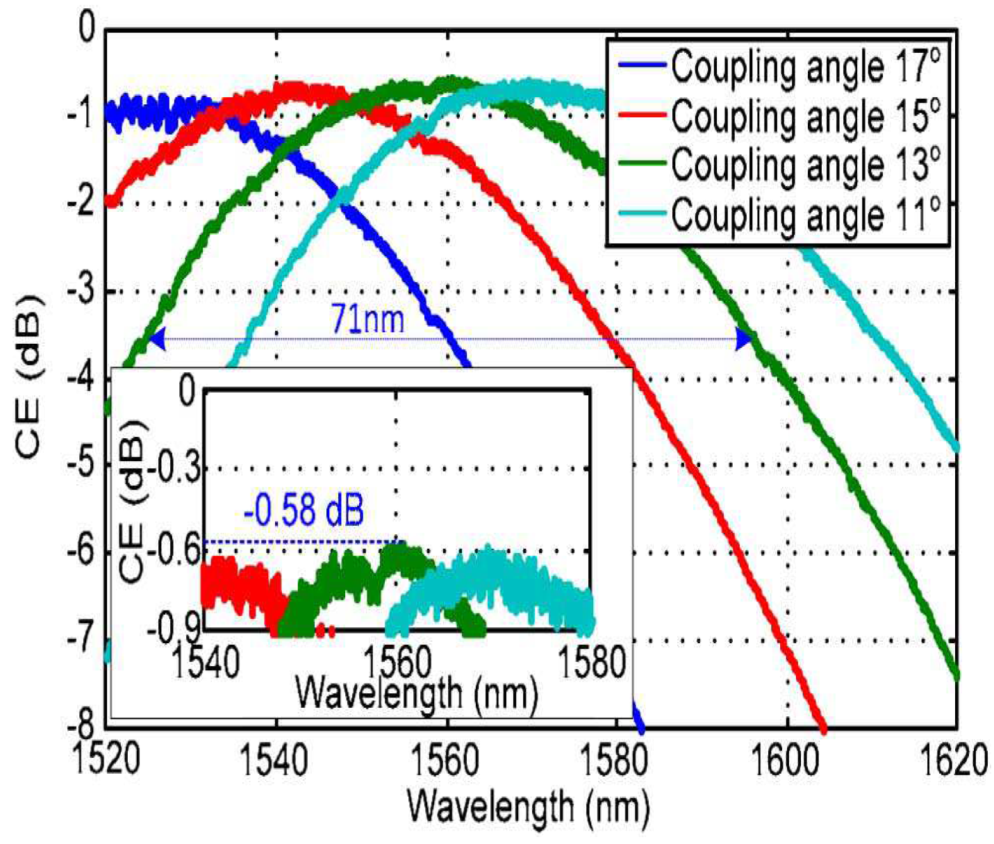
| Ref [25] | 0.58 | 71 | 1.56 | A | 13 | Full | Y |
| Taper Designs | Length (m) | Initial Width (m)-Final Width (m) | Coupling Efficiency Theoretical | Remarks | |
|---|---|---|---|---|---|
| Adiabatic Taper | Linear [39] | 150–500 | 10–0.5 | 65%–99% | Tradeoff between the taper length and coupling efficiency due to the adiabatic transition |
| Exponential [40] | 200 | 10–0.5 | 70% | ||
| Parabolic [41] | 200 | 10–0.5 | 80% | ||
| Efficient Adiabatic [42] | 120 | 10–0.5 | 98.3% | ||
| Non-Adiabatic | Complex Non-adiabatic [43] | 15.4 | 10–0.56 | 70% | Complexity in Fabrication |
| Lens-assisted [44] | 20 | 10–0.45 | -1 dB (TE) -5 dB (TM) Expt. | ||
| Discontinuous [45] | - | 10–0.45 | 90% | ||
| Compact Taper [46,47,48] | 15 | 10–0.5 | 92% | Robust to Fabrication errors, Broadband, Efficient | |
| SOI Coupler | Max CE (-dB) | Polarization 1 () (m) | Polarization 2 () (m) | Type (1D,2D) Focusing/Non-Focusing | PDL (-dB) |
|---|---|---|---|---|---|
| Ref [50] | 2 | (1.559) | (1.551) | 1D Non-focusing | High |
| Ref [51] | 5.8 | (1.54) | (1.535) | 2D Non-focusing | 0.2 |
| Ref [53] | 5.6 | (1.54) | (1.53) | 2D Focusing | 0.4 |
| Ref [54] | 3.2 | (1.492) | (1.492) | 2D Focusing | 0 |
| SOI Coupler | Max CE (-dB) () | Max CE (-dB) () | Polarization () (m) | Polarization () (m) | Bandwidth 3 dB (nm) () | Bandwidth 3 dB (nm) () |
|---|---|---|---|---|---|---|
| Ref [59] | 8 | 7 | (1.3) | (1.55) | - | - |
| Ref [60] | 6.5 | 6 | (1.485) | (1.53) | 30 | 30 |
| Ref [58] | 8.2 | 7.1 | (1.31) | (1.55) | 18 (1.5 dB) | 35 (1.5 dB) |
© 2018 by the authors. Licensee MDPI, Basel, Switzerland. This article is an open access article distributed under the terms and conditions of the Creative Commons Attribution (CC BY) license (http://creativecommons.org/licenses/by/4.0/).
Share and Cite
Nambiar, S.; Sethi, P.; Selvaraja, S.K. Grating-Assisted Fiber to Chip Coupling for SOI Photonic Circuits. Appl. Sci. 2018, 8, 1142. https://doi.org/10.3390/app8071142
Nambiar S, Sethi P, Selvaraja SK. Grating-Assisted Fiber to Chip Coupling for SOI Photonic Circuits. Applied Sciences. 2018; 8(7):1142. https://doi.org/10.3390/app8071142
Chicago/Turabian StyleNambiar, Siddharth, Purnima Sethi, and Shankar Kumar Selvaraja. 2018. "Grating-Assisted Fiber to Chip Coupling for SOI Photonic Circuits" Applied Sciences 8, no. 7: 1142. https://doi.org/10.3390/app8071142
APA StyleNambiar, S., Sethi, P., & Selvaraja, S. K. (2018). Grating-Assisted Fiber to Chip Coupling for SOI Photonic Circuits. Applied Sciences, 8(7), 1142. https://doi.org/10.3390/app8071142