1. Introduction
Because the era of the Internet of Things (IoT) has been accompanied by the rapid development of the semiconductor industry and communication technologies, the use of high-tech products, such as mobile phones and wearable devices, has been spreading widely in our daily lives. The printed circuit board (PCB) is one of the key components of such electronic devices. A PCB is a thin plate made by printing an electrically conductive circuit on an insulator.
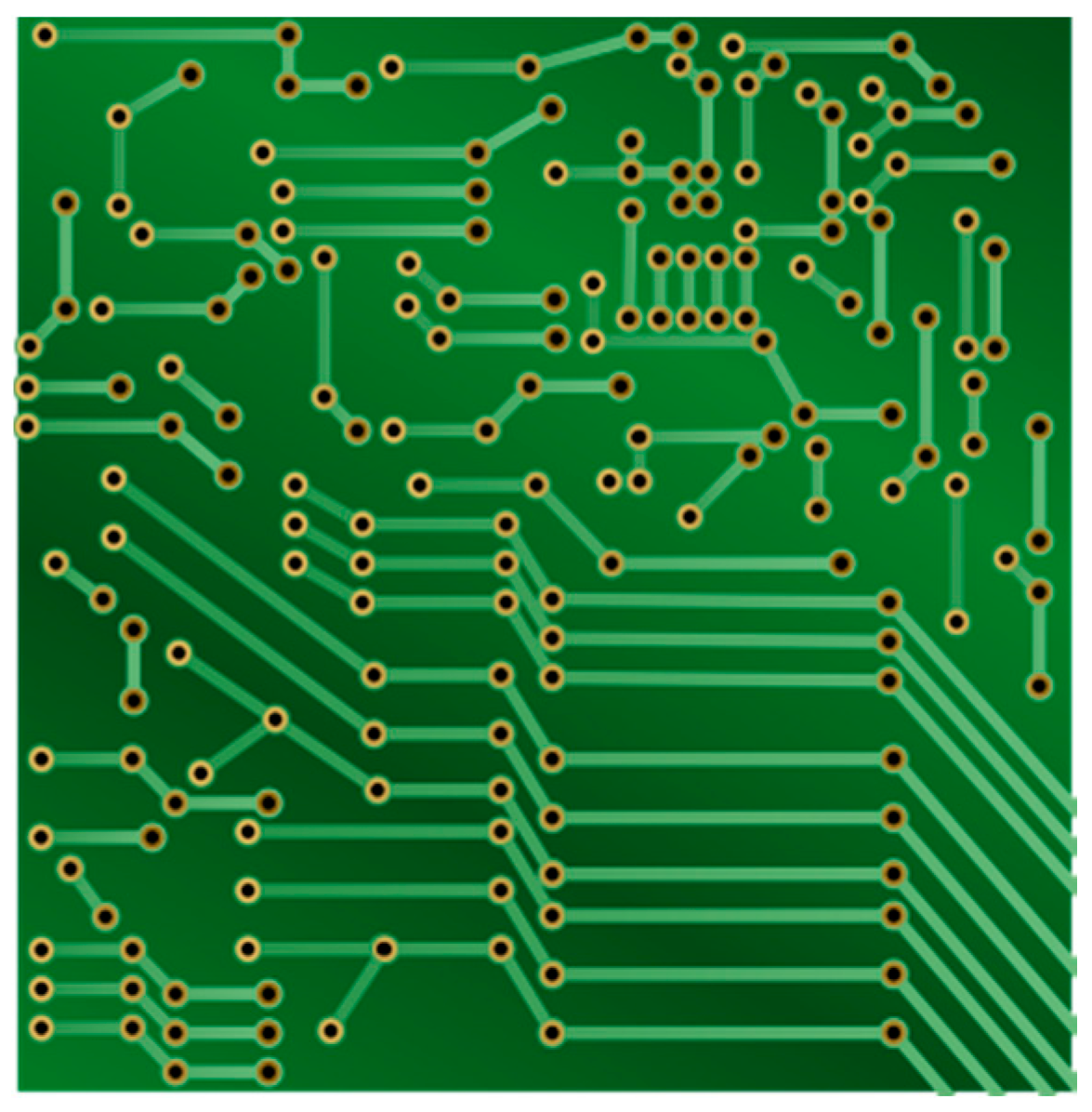
Figure 1 shows an image of a generic PCB. As shown in
Figure 1, a PCB connects to different parts electrically through a point-to-point wiring process.
In the past, handwork wiring led to frequent failures of the wire junctions and a short circuit as the wire insulation began to age. Furthermore, this type of work was conducted manually for inner-connecting components within the board. Such wiring, therefore, required a significant amount of time and effort. With advancements in technology, PCBs were developed for efficient and automated production. Because PCBs allow for the use of mass production, they allow devices to be smaller and lighter. In addition, they allow a high level of reliability at low production costs. Because of these advantages, most electronic devices use PCBs.
According to the recent trend of miniaturized and high-performance electronic devices, the demand for PCBs has increased substantially. The current PCB market has shown an average annual growth rate of 4%. Based on increasing demand, electronics manufacturers require perfect quality and a high level of accuracy from their PCB inspections to assure their competitive edge. To meet these quality requirements, PCB manufacturers conduct an inspection before proceeding to the main process. The PCB manufacturing process consists of many steps: cutting, inner layer etching, an automatic optical inspection (AOI), lay-up, lamination, etching, drilling, solder masking, routing, a bare board test (BBT), quality control, packing, and shipping, in that order. Before proceeding to the main processes, such as lamination and etching, faults in a PCB are detected during the AOI stage. An AOI is an automated visual inspection using an image comparison method. Most PCB manufacturers inspect their PCBs through the AOI process. The types of defects detected during the AOI process include scratches, improper etching, and open circuits. In particular, scratches are fatal defects because they have the potential to change the electrical properties and can result in a malfunction of the completed product.
There are typically three methods applied during the AOI process: a comparison reference (CR), non-reference verification (NV), and a hybrid approach (HA). The CR method compares an inspected image with a reference image. It measures any existing dissimilarities between the reference image and the inspected image. Thus, this method requires a reference image, and inspection is difficult without such an image. The NV approach tests the design rule of the PCB for detecting faults. It essentially verifies the widths of the insulators and conductors. However, this approach makes it difficult for users to design the rules as restrictions on the image features, and it cannot detect faults without such rules [
1]. The HA approach combines various types of CR and NV methods. That is, the approach utilizes a reference image or design rules to inspect a PCB image. However, it still does not solve the limitation of being unable to conduct an inspection without reference information. Because the circuits used in a PCB are diverse and complex, the reference information increases significantly, thereby decreasing the inspection’s efficiency. Therefore, additional studies are required to detect faults without reference information.
Numerous algorithms have been proposed to improve the accuracy of a PCB inspection. Such algorithms can be categorized into two approaches: referential and non-referential methods.
A referential method is based on a comparison between the inspected image and a reference image. To measure the dissimilarity between these two images, image subtraction and template matching techniques are used. Wu et al. proposed an inspection method based on a subtraction method [
2]. The image subtraction method compares both images using an XOR logic operator [
3]. The resulting image, which is obtained after this operation, contains only portions of a fault [
4]. Therefore, the reference image and the inspected image should be placed in a fixed position to compare both images. In addition, a reference image of the same size is required. Template matching is a technique for identifying the parts of the image that match the reference image. This method extracts the features of both the reference and inspected images. It then calculates the similarities of these features. One of the major disadvantages of template matching is that a large amount of information regarding the reference image must be used. Therefore, this method requires a mass storage device that can store all of the information. Moreover, the inspected images also have to be precisely matched for a comparison with the reference image [
5]. Acciani et al. suggested an inspection algorithm that extracts the wavelet and geometric features, and then detects a defect after learning the fault pattern using a neural network and k-nearest neighbors [
6]. When extracting the features of a PCB image, this method uses the maximum value of the correlation coefficients between the features of the reference image and the inspected image. This approach of applying machine-learning algorithms is called the learning-based model. The aim of this approach is to automatically detect faults through pattern recognition [
7]. In [
8], the authors proposed a defect detection method using feature matching for non-repetitive patterned images. The method first extracts features of both the reference image and the inspected image using a modified corner detector. It then detects a fault by finding a correspondence between two feature sets. Thus, the methods [
6,
8] still require a reference image to detect a fault.
A non-referential method, on the other hand, does not require a reference image. However, this method uses design rules. If the inspected image does not conform to the design specification standards, it is considered defective. Ye and Danielson suggested a verifying algorithm for minimum conductive and insulator trace widths [
9]. This algorithm uses morphological techniques, which are methods for processing binary and grayscale images based on shape. Morphological techniques do not require a predefined model of a perfect pattern because we can construct specific shapes in an image by choosing an appropriate neighborhood shape [
10]. However, this method has a disadvantage in that we should apply different pre-processing algorithms to check for faults in a PCB. In addition, it automatically increases the inspection time [
5]. Tsai et al. proposed a non-referential defect detection approach for bond pads [
11]. This approach restores the shape of the bond pads using Fourier image reconstruction. The method then evaluates the similarities and differences in the pad shape. However, the method has difficulty in reconstructing an original image of a PCB in the absence of a reference image because the shape of a circuit is quite varied and complex. Thus, the method is not suitable for detecting faults on a PCB. As mentioned earlier, a non-referential image analysis has certain limitations.
Rosten and Drummon proposed a very fast and high-quality corner detector using machine-learning techniques [
12]. This algorithm uses a decision tree to learn the properties of the corner points and determine which point is a corner point instead of directly counting the number of consecutive points of the same type. Pernkopf proposed an approach for the detection of three-dimensional faults on scale-covered steel surfaces [
13]. After extracting features, the approach uses a Bayesian network to learn the feature property and classify the faults. Classification research, which is learning the patterns of the extracted features through image processing, is actively carried out to diagnose skin cancer not only in manufacturing but also in dermatology [
14]. It is indispensable to extract meaningful features that can explain the properties of shape and color in order to effectively detect a melanoma [
15]. Roberta suggested a method to find meaningful features by combining three characteristics of shape, texture, and color [
16].
Based on the concept of a learning property, we propose a new non-referential method for fault detection by extracting features based on an image-processing method and learning the fault information using random forests. The proposed method utilizes features obtained through speeded-up robust features (SURF) to describe the fault information. Therefore, the method can detect a fault quickly and accurately without a reference image and without being affected by environmental changes, such as the size, rotation, and location of the PCB. The proposed method first extracts robust features using an image-processing technique and learns the fault pattern using an efficient classification technique utilizing high-dimensional data. We then calculate the probability and draw a weighted kernel density estimation (WKDE) map weighted by the probability and identify whether a fault has occurred.
The remainder of this paper is organized as follows: In
Section 2, the background of the proposed method is briefly reviewed.
Section 3 describes the procedure of the proposed inspection algorithm.
Section 4 presents the experimental results through a comparison of the receiver operating characteristic (ROC) curves. Finally, some concluding remarks are given in
Section 5.
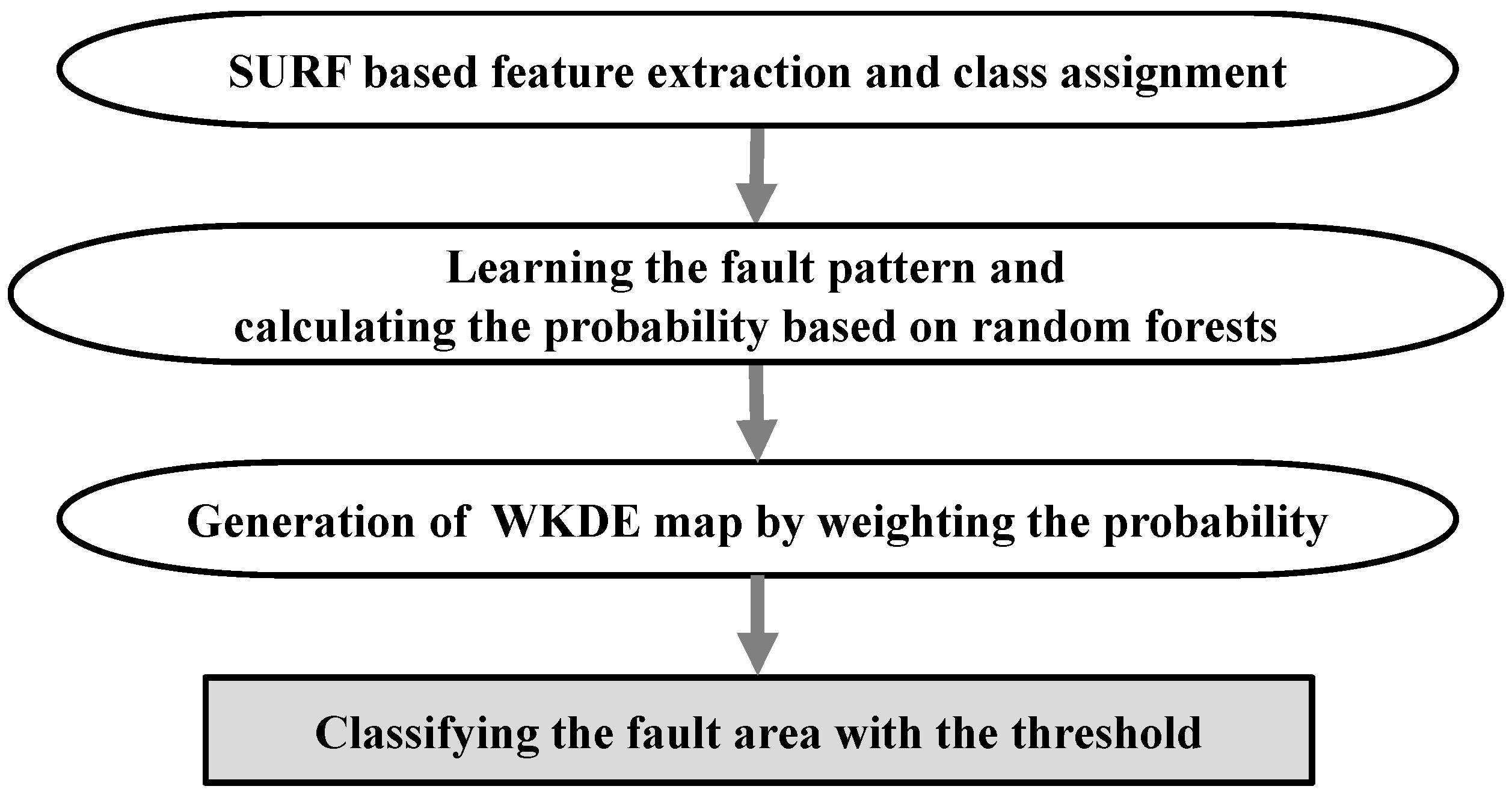
3. Proposed Method
Based on the algorithms described in
Section 2, we propose a scratch fault detection method, which is depicted in
Figure 4. First, SURF extracts the features of the PCB image. The extracted features are composed of a multivariate vector representing the properties found in the PCB image, such as an edge, blob, or curve. Because SURF also extracts the features in a scratch-defective edge, it is difficult to distinguish between a normal edge and a fault edge using only these features.
Hence, we assign a normal or fault class to the features using the coordinates of the features within a defective or normal area. We then learn the normal and fault properties using the multivariate vector and feature class and calculate the probability of each feature being classified as a fault class. We then generate a new weighted kernel density estimation (WKDE) map. Kernel density estimation (KDE) is a technique for estimating the density based on the coordinates. That is, KDE is a technique that considers the density of the features. To maximize the effectiveness of the features, the probability of affecting the spatial density is given as a weight to the KDE. Thus, we consider not only the properties but also the densities of the features. After generating a WKDE map, we can predict the fault area based on the WKDE value. The proposed method is described in more detail in the following subsection.
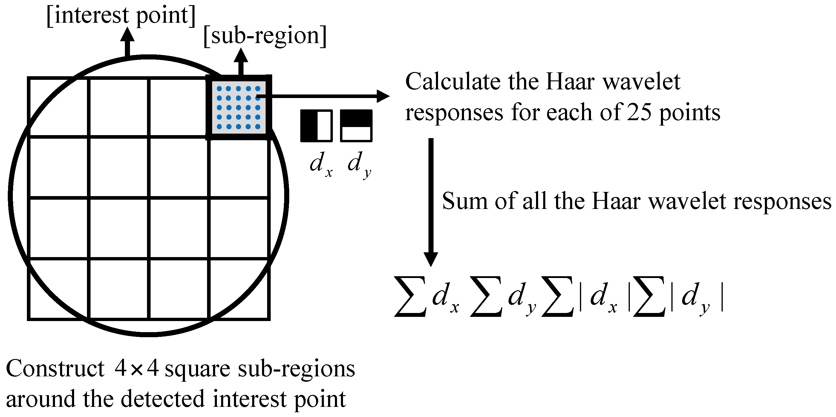
3.1. SURF-Based Feature Extraction and Class Assignment
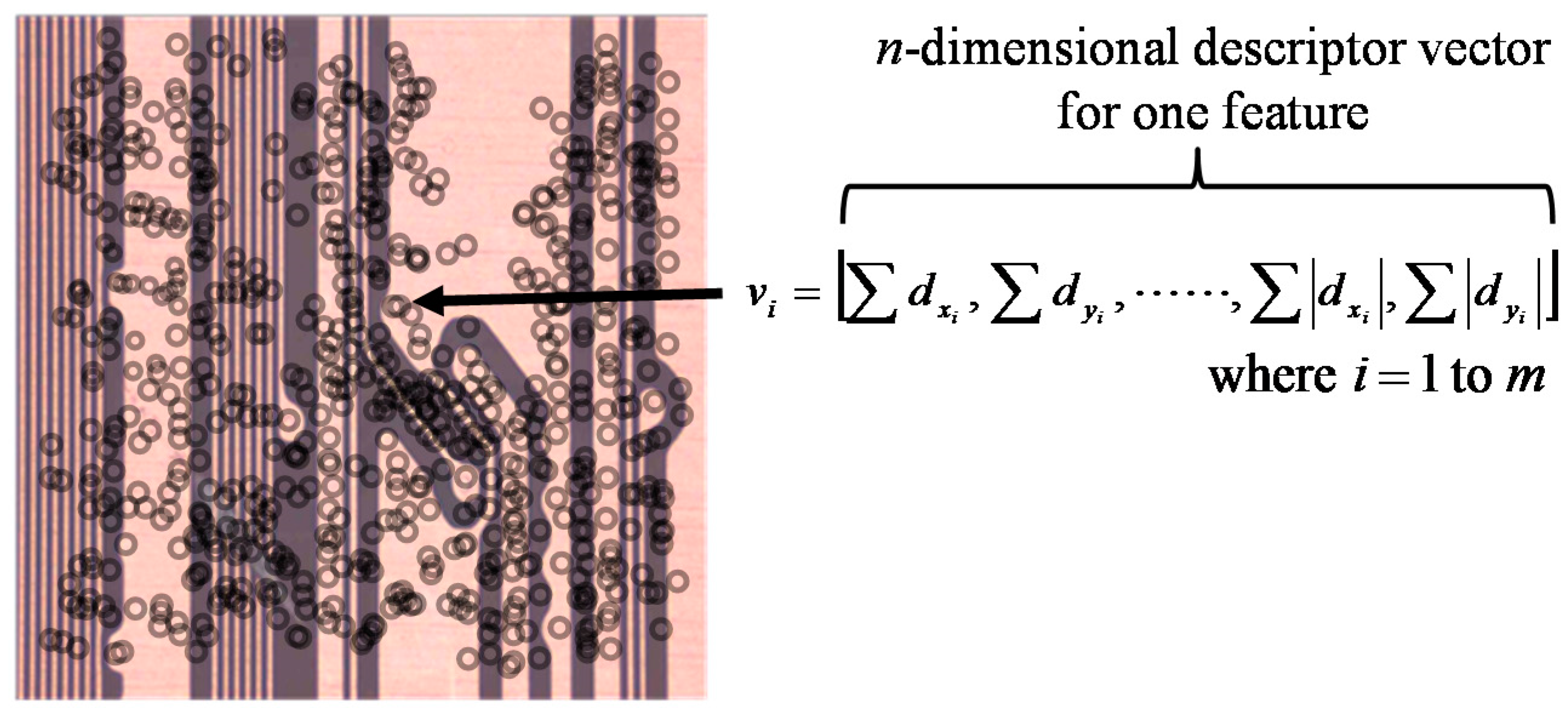
As the first step of the proposed method, SURF digitizes a PCB image as a vector. SURF then detects the features and extracts the descriptors in the form of a vector as mentioned in the previous section.
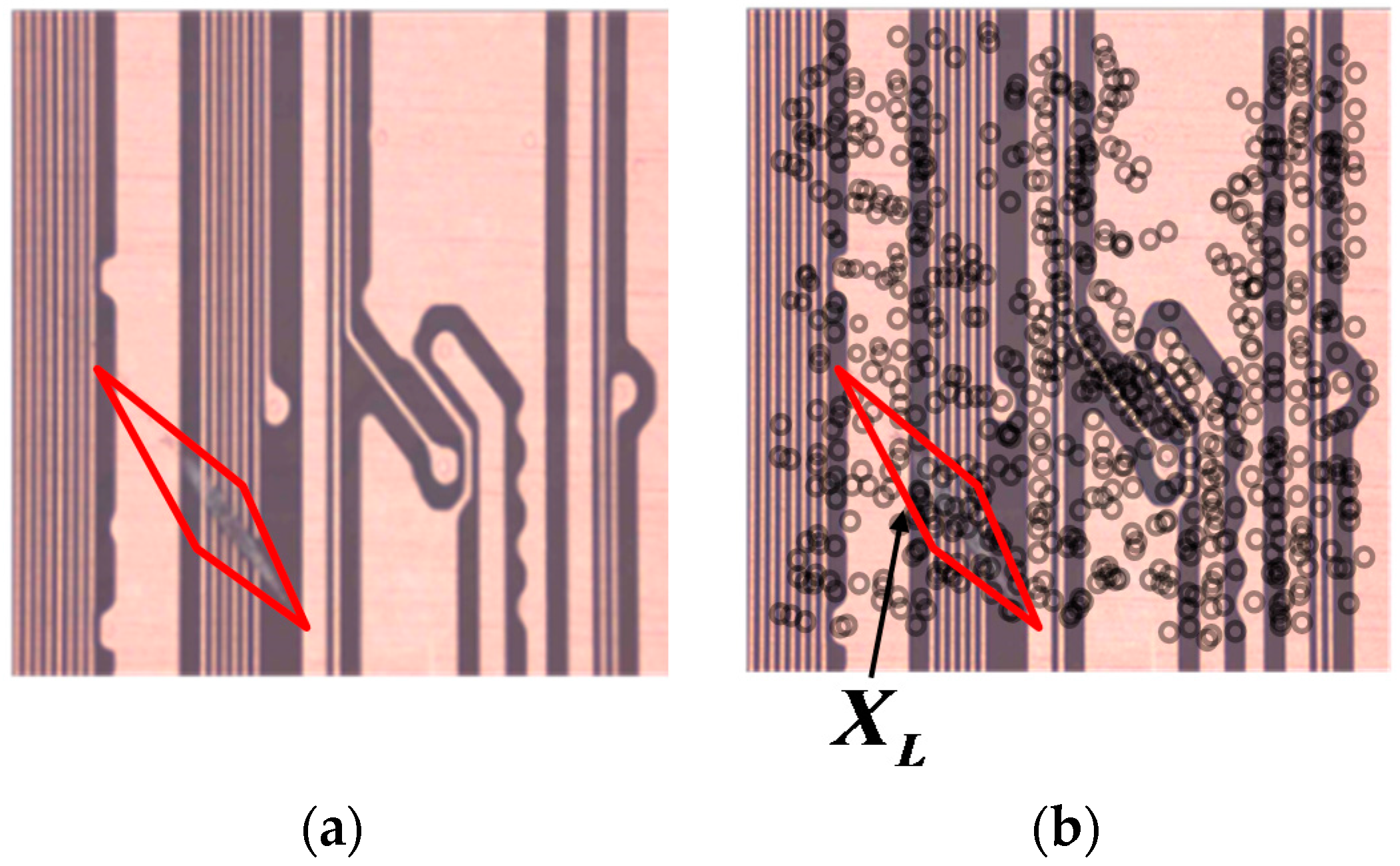
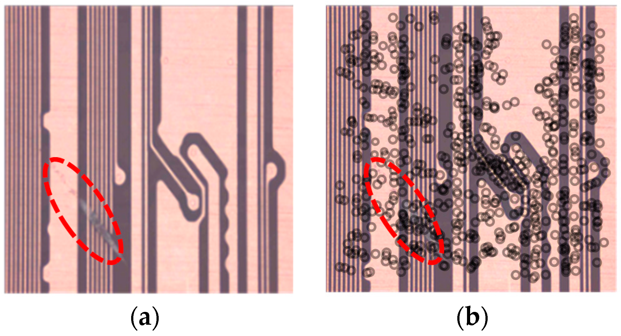
Figure 5a shows an example of an original PCB image. The circuits in the area inside the dotted line have a defective edge, whereas the other circuits have a normal edge. The extracted features are shown in the circles in
Figure 5b. As
Figure 5b illustrates, the features are obtained identically without discriminating between a defective edge and a normal edge. In other words, SURF cannot distinguish between a defective and a normal edge. Thus, we should learn the fault pattern of the features by setting the normal and fault areas and assigning classes to each feature.
As shown in
Figure 6a, we define a lozenge area with four points so that the fault area can be visually represented in the clearest manner. We can then consider the fault occurring in the lozenge area. We assign the features within the lozenge area in
Figure 6b to the fault class. The remaining features from areas other than the lozenge area are designated as being of a normal class through Equation (8).
where
indicates each feature composed using a multivariate vector and
is a set of features within the lozenge area.
3.2. Learning the Fault Pattern and Calculating the Probability Based on Random Forests
Given the class-assigned features, the following step is to handle fault patterns using a machine-learning algorithm. This method is based on the random forests method, which is a well-known ensemble learning model for classification. We first learn the fault pattern of the features. We use a 136-dimension input vector, , composed using extended descriptors and the information of each feature, such as its location and class, for a more precise description. The extended descriptors are computed by summing and separately for and . Similarly, and are split for and . Thus, the number of vector dimensions of the descriptors doubles to 128. After building the learning model by training the properties of the features, we can find the probability that each feature of an inspected image will be classified as a fault, which is calculated using Equation (7). Because the classes of the features are extremely imbalanced, most features are classified as normal. That is, the probability that the features will be estimated as a fault is considerably less than the probability that they will be predicted as normal. Consequently, because it is difficult to detect a fault area using only the results of the random forests, we should consider the density in addition to the map of the probability of being predicted as a fault.
3.3. Generation of WKDE Map by Weighting the Probability
This section describes how to apply the probability calculated in the previous section to generate a weighted kernel density estimation (WKDE) map, a technique that reflects the kernel density estimation (KDE). KDE is a probability density estimation method using a kernel function. In addition, it is a nonparametric method that is even applicable to high-dimensional data [
23]. The representative kernel functions include Gaussian, uniform, and Epachenikov functions [
24]. This paper uses a Gaussian kernel function to estimate the density.
After calculating the probability, we generate a WKDE map by giving the weight, , to the kernel function in order to complement any disadvantages as mentioned earlier. Because the PCB features have - and -axis coordinates, this method uses the weighted multivariate kernel density estimation.
Let
be the coordinates of the PCB features. The WKDE value is denoted through Equation (9) [
25].
where
is the total number of PCB features,
is a scaled kernel that controls the smoothness of the estimate, and
is the probability of being classified as a fault. In addition,
is a Gaussian kernel function.
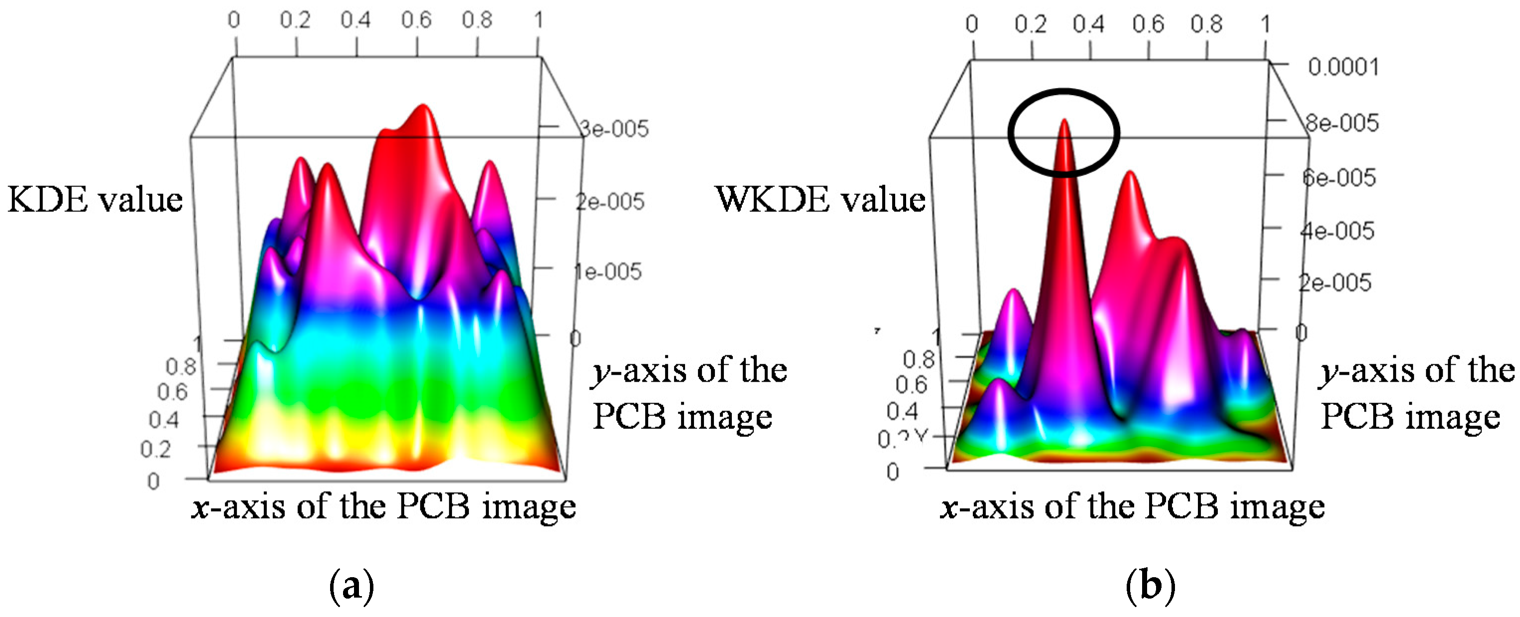
KDE and WKDE maps were drawn using the features extracted from the PCB image in
Figure 5 as shown in
Figure 7. The
and
axes in the KDE and WKDE maps represent the coordinates of the features. The
axis of the KDE map indicates the KDE value, which is calculated based on the coordinates of each feature, whereas the
axis of the WKDE map is the WKDE value obtained by weighting the probability to the KDE. Because the KDE considers only the density, it has a high KDE value in areas where many features are extracted regardless of the defective area as shown in
Figure 7a.
Consequently, it is difficult to distinguish between a normal area and a fault area on the KDE map. On the other hand, the WKDE value, which reflects the probability, increases when the probability of each feature being classified as a fault is higher than the probability of the other features. Otherwise, the WKDE value decreases because there is a relative difference between the probabilities. The area marked with a circle in
Figure 7b has a relatively high WKDE value owing to the weight. That is, because the marked area is densely concentrated with fault features, the WKDE value of this area is higher than the KDE value. In addition, the KDE values in the remaining areas are randomly distributed, but decrease significantly after being weighted. Thus, we can predict the marked area as a fault area.
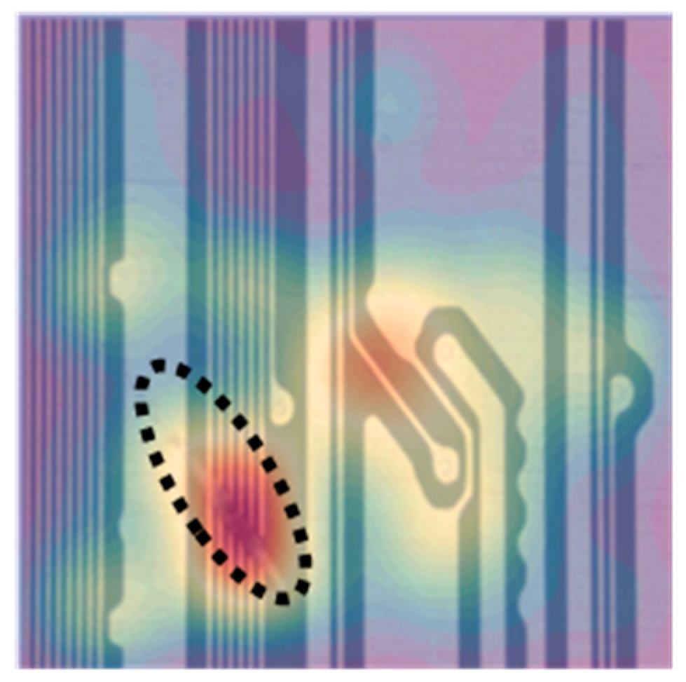
Figure 8 shows a three-dimensional (2-D) WKDE map overlapping the original image (
Figure 5a). In the 3-D WKDE map, it is difficult to intuitively recognize the coordinates of a feature. Thus, we convert the 3-D image into a two-dimensional (2-D) image to prove that the marked area in
Figure 7b is consistent with the real fault area. The area within the dotted line in
Figure 8 indicates where the actual faults occur, whereas the shaded area is an area predicted as a fault because the WKDE value exceeds the threshold. As
Figure 8 shows, we can confirm that the shaded area matches the dotted area. Therefore, we monitor the WKDE value and predict the features as being a fault if the WKDE value exceeds the threshold. In this paper, we set a WKDE value of higher than 1% as the threshold. However, the threshold changes according to the process yield or to past experience.
4. Experimental Results
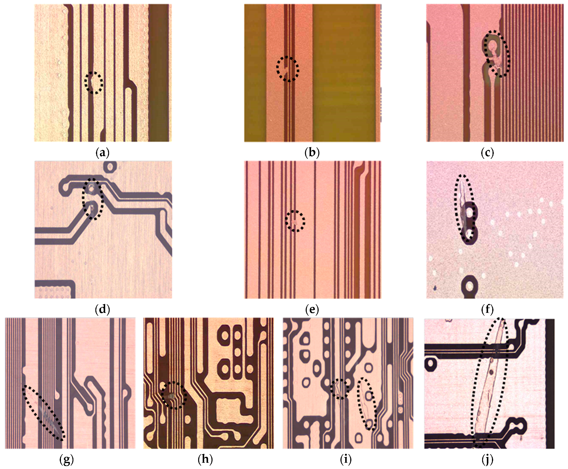
The present experiment used PCB image data to verify the proposed method. PCB images were collected from a battery manufacturer in Korea. We obtained 10 PCB images by selecting a fault image with a particular scratch property. As shown in
Figure 9, the scratch fault, which is indicated by the dotted line, has a fine and thin form, indicating that the circuit may be broken. Because a scratch defect may prevent a current flow within the circuit, it has a significant impact on the PCB quality. Therefore, this paper analyses PCB images with a scratch defect.
We first extracted the features in the 10 PCB images using SURF. We then assigned a class to each feature by designating the defective area and organized the 136-dimension input vector including information such as the coordinates and class. The data were then divided into the test set and training set for learning purposes. This experiment applied a 10-fold cross validation using the 10 images. For example, nine images are used for training, and the remaining image is used for testing. Next, we obtained the WKDE value for each of the 10 PCB images as mentioned in
Section 3.
To diagnose a fault area, statistical process control (SPC) can be applied to monitor the WKDE value. SPC is a method of quality control that uses statistical methods based on the distribution of data [
26]. However, there is no assumption regarding the distribution of the features. For this reason, this research cannot utilize SPC. Hence, a binary classification was applied based on a single continuous WKDE value to examine whether a feature is a fault. The features were classified by comparing the WKDE value with a threshold
, which is called the cut-off value. A feature was classified as a fault if
and was classified as normal otherwise.
The appropriate threshold can be chosen based on various criteria [
27]. Thus, we conducted the experiments using a variety of thresholds, and adopted an appropriate threshold based on a receiver operating characteristic (ROC) curve, which is a tool for demonstrating the performance of a classifier. An ROC curve is a threshold-independent technique for evaluating the performance of a model and represents the relationship between the model’s sensitivity and specificity [
27]. In this study, the ROC curve was drawn based on the true- and false-negative rates. The ROC curve for a good model achieves a high true-negative rate whereas the false-negative rate is relatively small. Therefore, the performance of a model can be evaluated by comparing the area under the ROC curve (AUROC). Robust models have an AUROC of close to 1.0, whereas poorer models have an AUROC near 0.5, and worthless models have a value of less than 0.5 [
28].
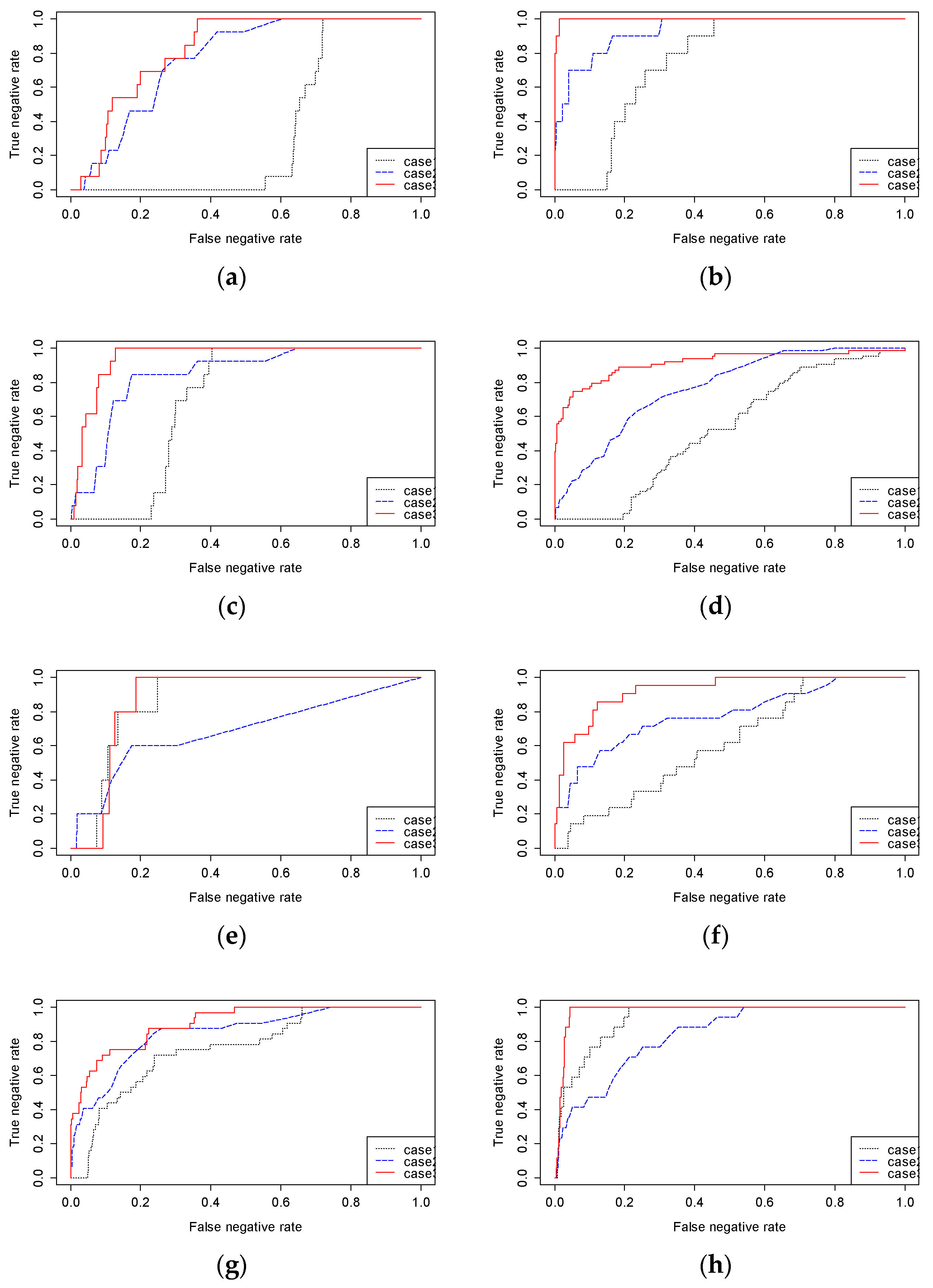
To demonstrate that both the probability and density of the features have to be considered for detecting a fault, this paper compares the performances of three different methods: (1) monitoring only the probability (Method 1), (2) using a KDE map (Method 2), and (3) using the proposed WKDE map (Method 3). Each method applies binary classification to detect a fault. Method 1 detects a fault area by monitoring only the probability obtained by the random forests. An area is determined as a fault area when the probability of the feature being a fault exceeds a certain threshold. That is, this method does not consider the density of the features. Method 2 identifies a defect by considering only the density of the features without taking into account the probability. Thus, it monitors the KDE value. Finally, Method 3, the proposed method, detects a fault by monitoring the WKDE value. This method considers both the properties of the features and their density. Finally, we draw an ROC curve to compare the performances of the three methods.
Figure 10 shows the ROC curves for the three methods. A method in which the AUROC is close to 1.0 detects a PCB fault more precisely. As can be seen, the AUROC of Method 1 is larger than that of Method 2 for 6 of the 10 images. However, the AUROC of Method 1 is less than that of Method 3 for all 10 images. Thus, the performance of Method 1 is not proper for detecting faults. Although Method 2 outperforms Method 1 for certain images, it has a poorer level of performance than Method 3. On the other hand, Method 3 outperforms the other methods, and its AUROC is close to 1.0 for all images. Therefore, Method 3 is appropriate for detecting a scratch fault on a PCB.

