Article

Multi-Azimuth Failure Mechanisms in Phosphor-Coated White LEDs by Current Aging Stresses

1
Department of Electronic Science, Fujian Engineering Research Center for Solid-State Lighting, Xiamen University, Xiamen 361005, China
2
Xiamen Products Quality Supervision & Inspection Institute, National Testing Center for LED Application Products, Xiamen 361004, China
3
Changtai Tianming Physics Research Institute, Changtai 363900, China
4
Institute of Electro-Optical Engineering, National Chiao Tung University, Hsinchu 30010, Taiwan
5
Department of Electronic Engineering, Xiamen University, Xiamen 361005, China
*
Authors to whom correspondence should be addressed.
These authors contributed equally to this work and should be considered co-first authors.
Appl. Sci. 2018, 8(4), 610; https://doi.org/10.3390/app8040610
Submission received: 14 March 2018 / Revised: 2 April 2018 / Accepted: 2 April 2018 / Published: 12 April 2018
(This article belongs to the Special Issue Highly Efficient UV and Visible Light Sources)

Abstract

:
We have experimentally analyzed multi-azimuth degradation mechanisms that govern failures of commercially-available high-power (1 Watt) phosphor-coated white (hppc-W) light-emitting diodes (LEDs) covered with peanut-shaped lenses under three current-stress aging (CSA) conditions. Comprehensive analyses focus on photometric, chromatic, electrical, thermal and packaging characteristics. At the packaging level, (a) the decrease of the phosphor-conversion efficiency; (b) the yellow-browning of the optical lens; and (c) the darkening of the silver-coated reflective layer deposited with extraneous chemical elements (e.g., C, O, Si, Mg, and Cu, respectively) contribute collectively to the integral degradation of the optical power. By contrast, Ohmic contacts, thermal properties, and angles of maximum intensity remain unchanged after 3840 h aging in three cases. Particularly at the chip level, the formation of point defects increases the number of non-radiative recombination centers, and thus decreases the optical power during aging stages. Nevertheless, in view of the change of the ideality factor, the Mg dopant activation and the annealing effect facilitate the increase of the optical power in two specific aging stages (192 h~384 h and 768 h~1536 h). This work offers a systematic guidance for the development of reliable LED-based light sources in general-lighting areas.

1. Introduction

The solid-state lighting (SSL) technology is regarded as the next-generation lighting approach, and exhibits great advantages of energy-saving, environmental-friendliness and smart lighting among others [1,2]. It is typically represented by white light-emitting diodes (LEDs), especially for the high-power phosphor-coated white (hppc-W) LEDs, which enjoy additional advantages, such as long lifetime, color-tunable property and high luminous efficiency [3,4].
However, room for improvement remains, including the internal quantum efficiency of the active region [5,6], the light-extraction technology [7], the current-flow design [8], the minimization of resistive loss [9], the electrostatic discharge stability [10], and the color-rendering property via the color mixing [11]. Aside from these improvements, various stress-inducing degradation tests, by means of temperature, current, static charge, optical radiation, and moisture, have been developed [12,13,14]. In some cases, two or more types of stresses are combined to accelerate the aging process for hppc-WLEDs [15,16].
As state-of-art failure-generating methods, high-temperature stresses and high-current stresses are regarded as the most commonly-used approaches that accelerate the optical degradation [17,18]. The former under various environmental temperatures have been carried out by several authors [19,20,21]. Among them, thermal stresses can primarily lead to the optical power decay for the degradation of the packaging system, such as the detachment of the contact metallization [19], the yellowing and fracture of the optical lens [20], and the degradation of phosphor mixtures [21]. Although current stress has also been applied to testing the degradation of LEDs, they may result in the optical degradation due to the deterioration at the chip level, such as the crystal defect formation in the epitaxial layer [22] and the reactivation of Mg dopants [23]. Since the current stress is usually accompanied by spontaneous thermal effects especially under high current stresses, investigating the degradation of hppc-WLEDs has become significant and practical. Furthermore, studies of current stresses that include photometric, chromatic, electrical, thermal, and packaging characteristics have been rarely reported in literatures.
In this article, comprehensive multi-azimuth failure analyses on hppc-WLEDs with peanut-shaped lenses at the chip level and the packaging level under 350 mA, 550 mA and 750 mA are presented. Particularly, peanut-shaped lenses offer the optical uniformity and large-view-angle light spatial distributions.

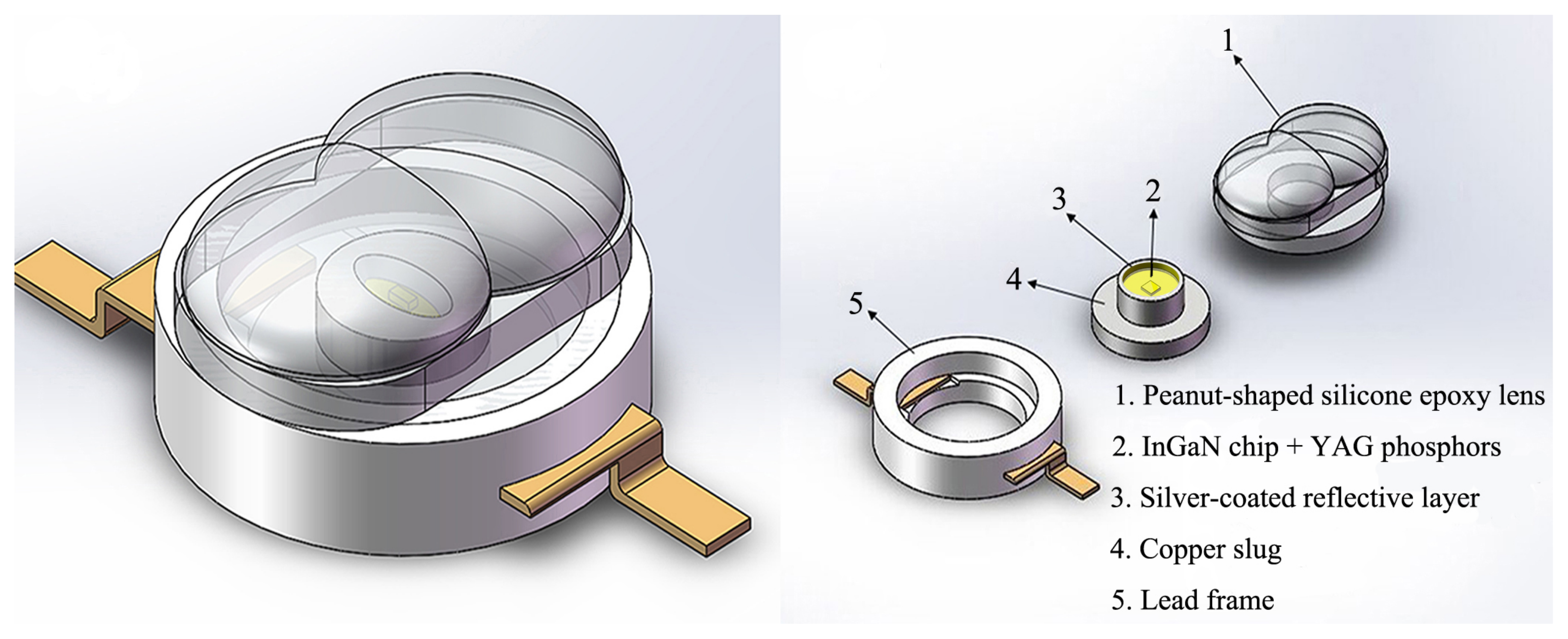
2. Experimental Methodology

Each of hppc-WLEDs consists of a blue InGaN LED chip (with an area of 1 mm × 1 mm), yellow YAG: Ce 3 + yellow phosphors, a silicone epoxy lens, a silver-coated reflective layer, and other packaging materials, as schematically shown in Figure 1 [24]. Three CSAconditions (T = 25 C, I = 350 mA (CSA-1), T = 25 C, I = 550 mA (CSA-2), and T = 25 C, I = 750 mA (CSA-3), respectively) are considered in these experiments. Thirty samples are divided into three groups (each group contains 10 samples) corresponding to three aging conditions. After aging tests, all samples are cooled down in the air for more than 5 h to release the remaining thermal energy prior to following measurements [25].
All instruments used in the experimental study are listed in Table 1. Specifically, a spectrometer (Spectro-320e, Instrument Systems Inc.), with a 500 mm integrating sphere (ISP-500, Instrument Systems Inc.) and an angular distribution analyzer (LEDGON 100, Instrument Systems Inc.), is employed to measure integral and angular spectral power distributions (SPDs) of these hppc-WLEDs. Therefore, photometric and chromatic analyses can be performed after relevant parameters are obtained from SPDs. The thermal resistance can be measured by a transient thermal tester (T3Ster 2000/100, MicReD Ltd.) with an accuracy resolution within 0.1 C. An electric source meter (Keithley 2611, Keithley Inc.) is used to drive samples, and to measure their electrical properties, such as current-voltage (I-V) characteristics and series resistances. Transmissivities of silicone epoxy lenses and reflectivities of silver-coated reflective layers are measured by adopting a 150 mm integrating sphere (ISP-150, Instrument Systems Inc.) with the same spectrometer mentioned above. During measurements, a white LED, as the light source, is placed on a heat sink regulated by the temperature controller (Keithley 2510, Keithley Inc.). In addition, a field emission scanning electron microscopy (FE-SEM, Sigma-HD, Zeiss Ltd.) attached with an energy dispersive spectrometer (EDS, X-Max N , Oxford Instruments Ltd.) is employed to detect and analyze microstructural and compositional changes on surfaces of silver-coated reflective layers.

3. Results and Discussions

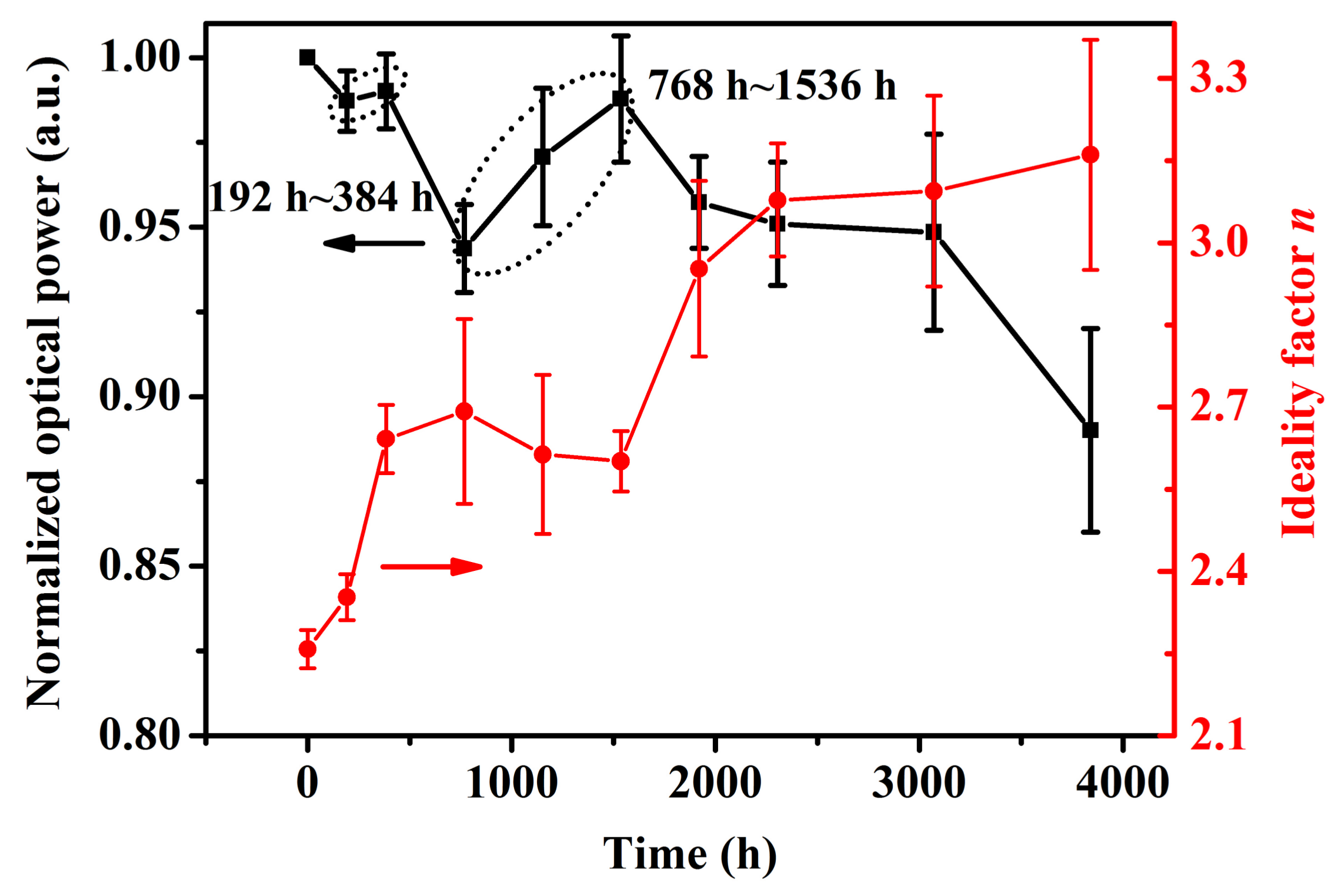
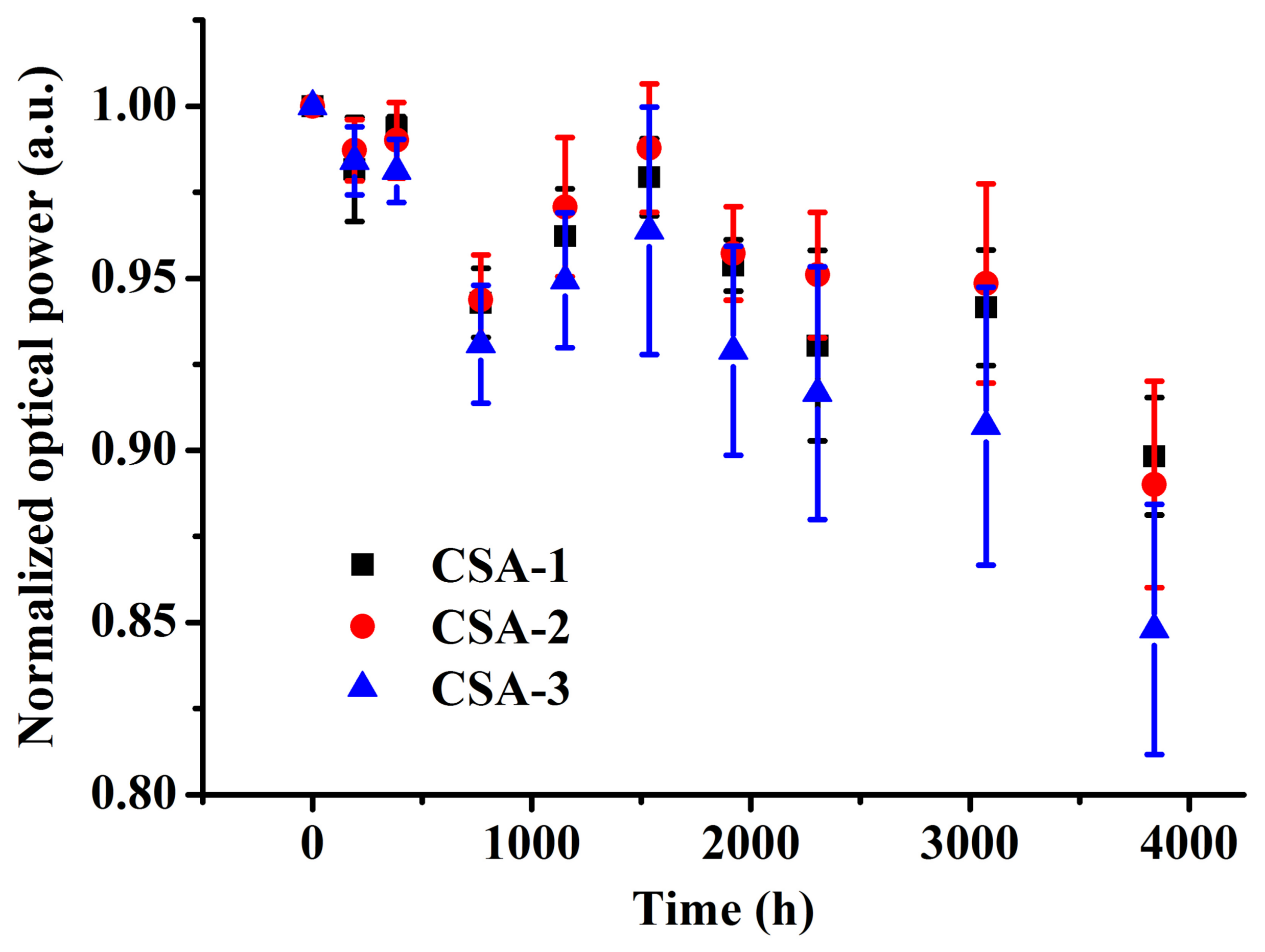
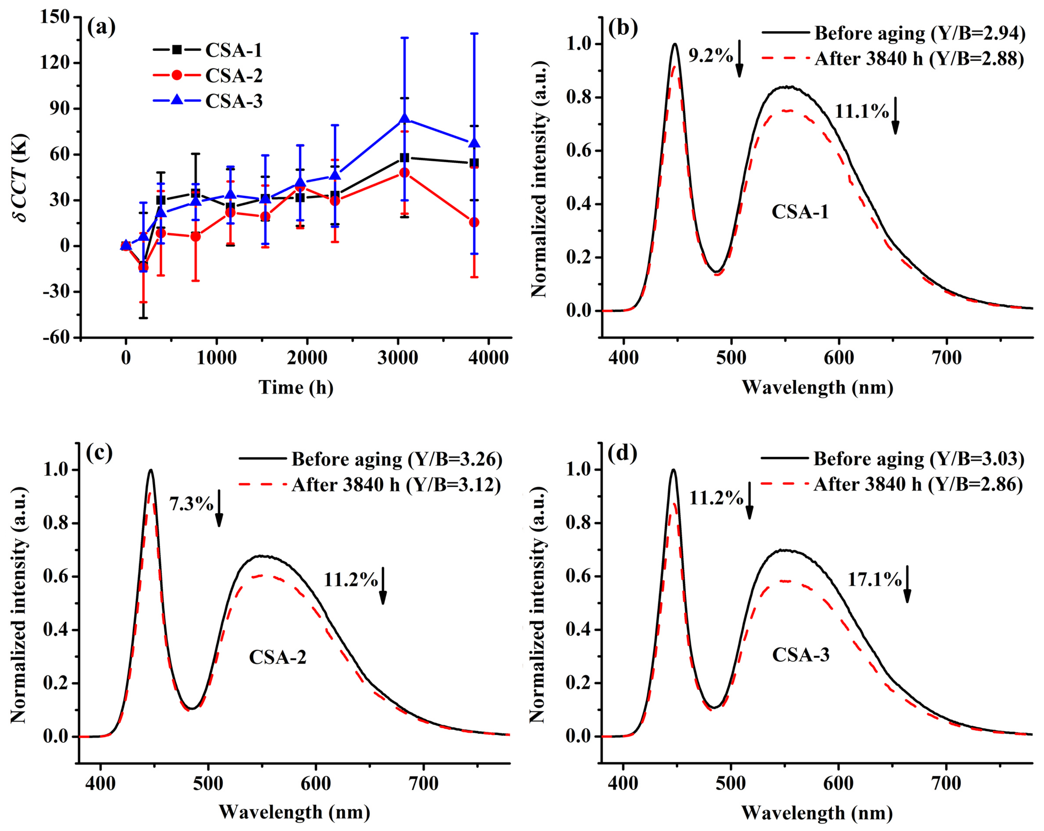
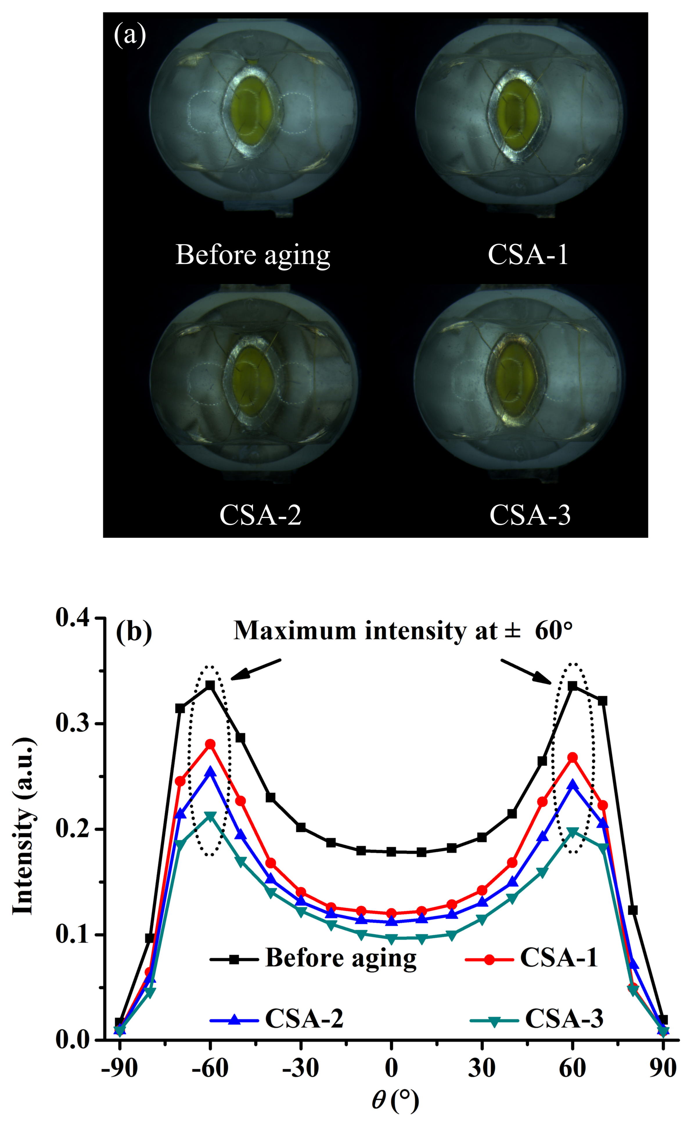
3.1. Photometric and Chromatic Analyses

Figure 2 depicts optical decays of hppc-WLEDs, measured at 350 mA and 25 C of the heat-sink temperature, for CSA-1, CSA-2, and CSA-3, respectively. As observed from Figure 2, significant optical decays occur in CSA-3 after aging for 3840 h, indicating that high current stresses will induce severe optical decays. Average optical decays after aging for 3840 h in three cases are estimated as 10.2%, 11.0%, and 15.2%, respectively.
To illustrate the change of the correlated color temperature (CCT) [26], we desire to introduce a parameter, δ C C T , which can be written as
δ C C T = C C T [ a f t e r ] C C T [ b e f o r e ] ,
where C C T [ b e f o r e ] and C C T [ a f t e r ] denote the CCT value before and after aging, respectively. Figure 3a plots the variation of CCT as a function of time. As observed, values of δ CCT increase as time elapses, but with mild variations. Specifically, after aging for 3840 h, all values of δ CCT in three cases lie within 200 K. Figure 3b–d show measured SPDs in three cases prior to and after aging. Both blue and yellow emissions decrease simultaneously after 3840 h aging. Optical decays of blue and yellow emissions are separately illustrated in these figures. In all three cases, severe optical degradations can be observed from yellow emissions relatively to blue counterparts. Especially in CSA-3, the optical decay reaches 12.2% for the blue emission and 17.1% for the yellow emission. For clear illustration, we calculate the ratio of the yellow optical power to the blue optical power, namely Y/B = P y e l l o w / P b l u e , which indirectly describes the phosphor-conversion efficiency (PCE) of hppc-WLEDs [27]. Values of Y/B are also shown in Figure 3b–d. Changes of Y/B are estimated as 2.0%, 4.3%, and 5.6% for CSA-1, CSA-2, and CSA-3, respectively. They imply that PCE slightly decreases after aging, because of the wavelength shift of blue LED chips after 3840 h aging [28]. The higher the aging current becomes, the more decrease PCE exhibits. Therefore, we conclude that the decrease in PCE during CSA tests leads to optical decays for these hppc-WLEDs.

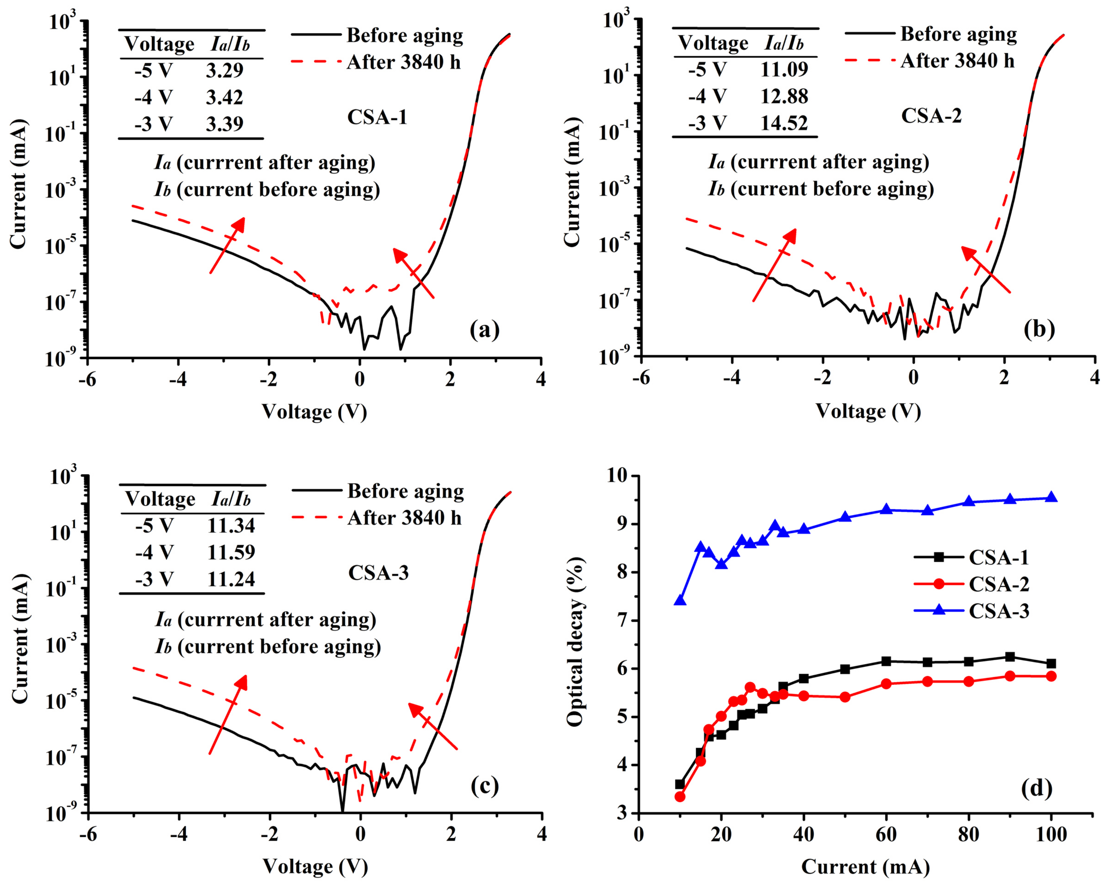
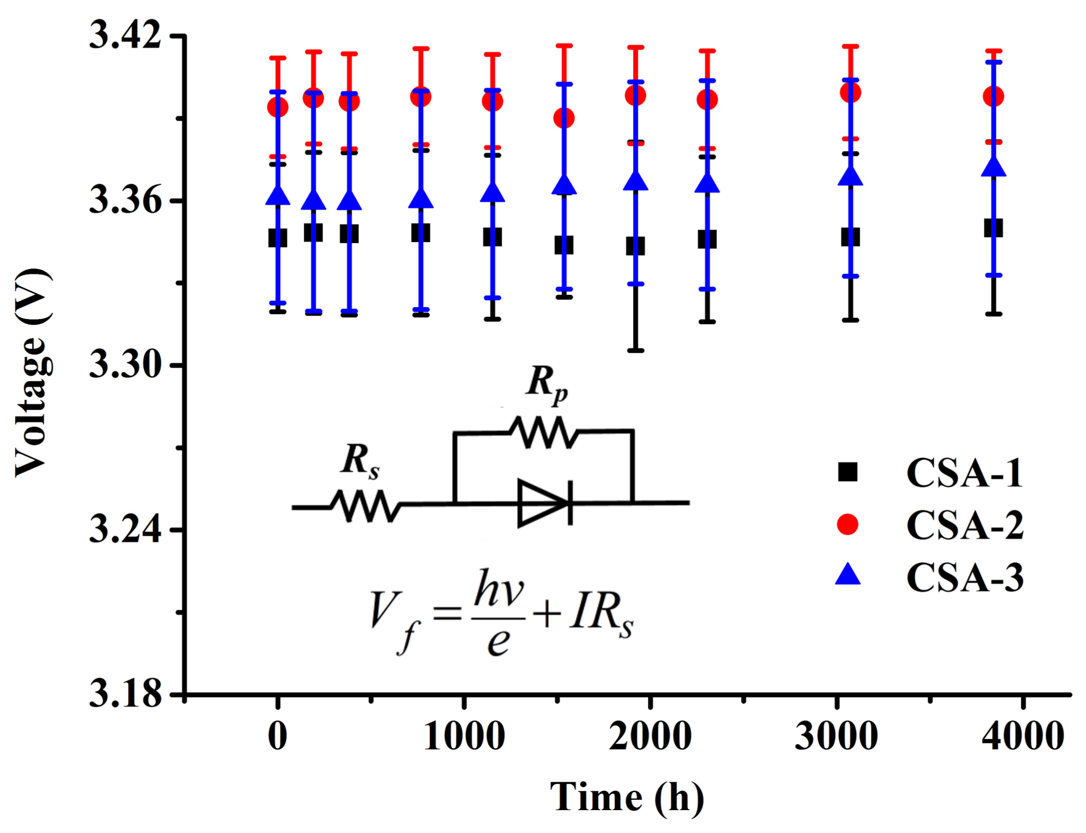
3.2. Electrical Analyses

Prior to and after aging for 3840 h, I-V curves of hppc-WLEDs nearly consolidate in all three cases for V f > 2.5 V (Figure 4a–c). These phenomena attest that indistinguishable deterioration of Ohmic contacts is observed in all aging stages. However, when V f < 2.5 V, leakage currents at reverse bias and low forward bias are found to increase after aging processes, manifesting the generation of shunt paths [29]. This undesirable generation originates from the birth and the propagation of nitrogen vacancies [30,31], which behave as non-radiative recombination centers, and weaken the optical power. Ratios of the current after 3840 h aging to the current before aging ( I a / I b ) at three representative voltages (−5 V, −4 V, and −3 V, respectively) are calculated in insets of Figure 4a–c. Large changes of I a / I b occur in CSA-2 (Figure 4b) and CSA-3 (Figure 4c), indicating that numerous shunt paths are generated after the high-current aging.
We also compare optical decays at various currents, which range from 10 mA to 100 mA in three cases. Results, depicted in Figure 4d, reveal that the optical decay increases as the testing current increases. Because both spectral shifts of the blue emission and the Joule heating in LED devices become prominent at high currents, further PCE decreases emerge [32]. Therefore, as PCE decreases, optical decays of total white lights increase.
Forward voltages measured at 350 mA and series resistances (according to the equation in the inset in Figure 5, where V f denotes the forward voltage, h the Planck constant, h v the photon energy, e the elementary charge, R s the series resistance, and I the electrical current) remain almost the same during aging periods in three cases (Figure 5), indicating again that Ohmic contacts remain unchanged after aging. However, at the same aging stage, voltages in CSA-2 exhibit larger values than those in other two cases. Apart from Ohmic contacts, it is generally believed that high current stresses will induce severe degradations in the active region of LED chips [33]. Nevertheless, considering the change of normalized optical power in Figure 2, where the optical power in CSA-2 also appears larger than other two cases except in two aging stages (384 h and 3840 h), we conjecture that the degradation of LED chips in CSA-2 should be mitigated in comparison with that of LED chips in CSA-1 and CSA-3.
To further study degradation mechanisms in chips from I-V characteristics, we select the result of devices in CSA-2 as an example. Figure 6 illustrates the degradation of the optical power measured at 350 mA (black square) and the corresponding change of the ideality factor n (red circle), which is computed via the I-V curve fitting by using the Sah-Noyce-Shockley model [34]. In general, point defects, such as nitrogen and gallium vacancies, inevitably assist electrons to enter quantum wells via the tunneling effect involving the non-radiative recombination process [35], thus increasing the value of n. Specifically, the normalized optical power overall decreases except in two anomalous periods (192 h~384 h and 768 h~1536 h), whereas the trend of the ideality factor appears almost oppositely.
Based on this reciprocity, it is plausible to create a reciprocal relationship between the normalized optical power and the ideality factor, exemplified by P = C 1 + C 2 /n, where P denotes the normalized out power; n the ideality factor; and C 1 and C 2 are constants to be determined. However, the detailed study of this plausibility belongs to the future work and will be omitted here. In the first anomalous period (192 h~384 h), the normalized optical power undergoes an increase due to the improvement of the effective carrier concentration reactivated by Mg dopants in the p-GaN [36]. In the second anomalous period (768 h~1536 h), the optical power increases inversely due to the annealing effect [37], which eliminates a portion of defects after the administration of the long-term high-current stress. Therefore, the annealing effect dominates this period, leading to the increase in the normalized optical power as well as the decrease in the ideality factor.

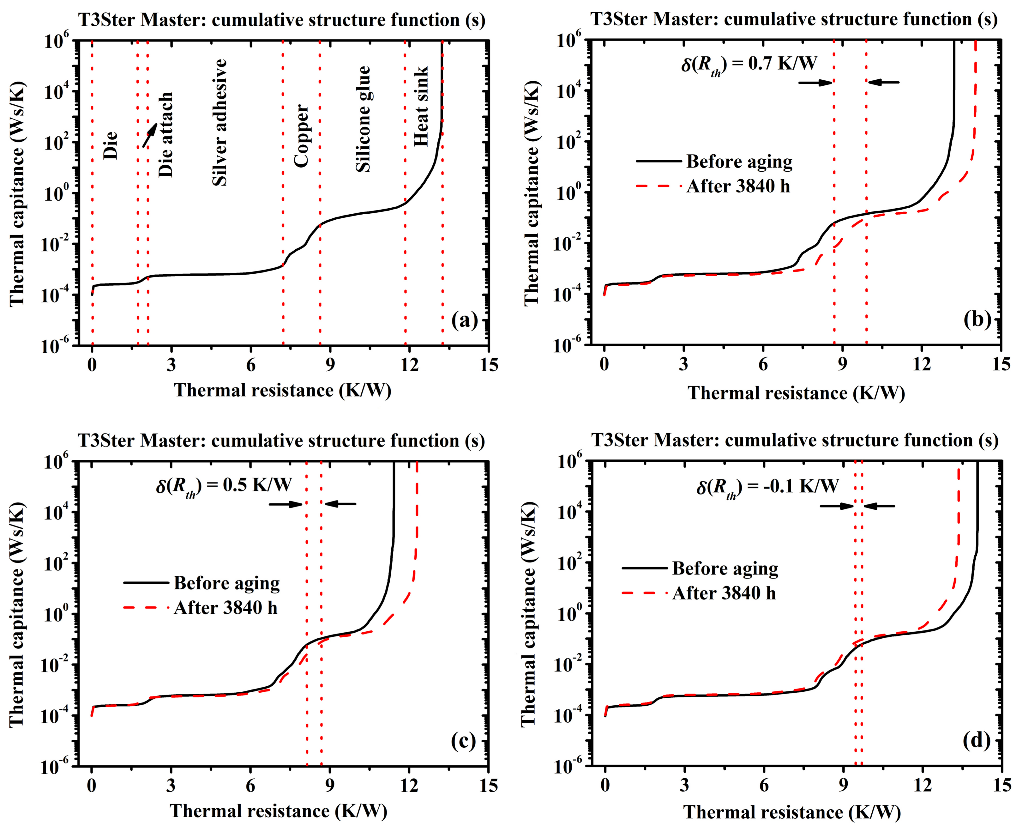
3.3. Thermal Analyses

We also perform thermal analyses on these hppc-WLEDs. Thermal resistances of samples are measured by the transient thermal tester (T3Ster). Based on the cumulative structure function by T3Ster software, plotted in Figure 7a, we can discern different thermal resistances in components of LEDs, including the die, the die attach, the silver adhesive, and the copper, respectively. Figure 7b–d show cumulative structure functions of hppc-WLEDs before and after aging for 3840 h in three cases. In comparison with respective initial values of thermal resistances, only small alterations ( δ ( R t h ) < 1 K/W) can be observed, indicating that the thermal property remains unchanged in three cases.

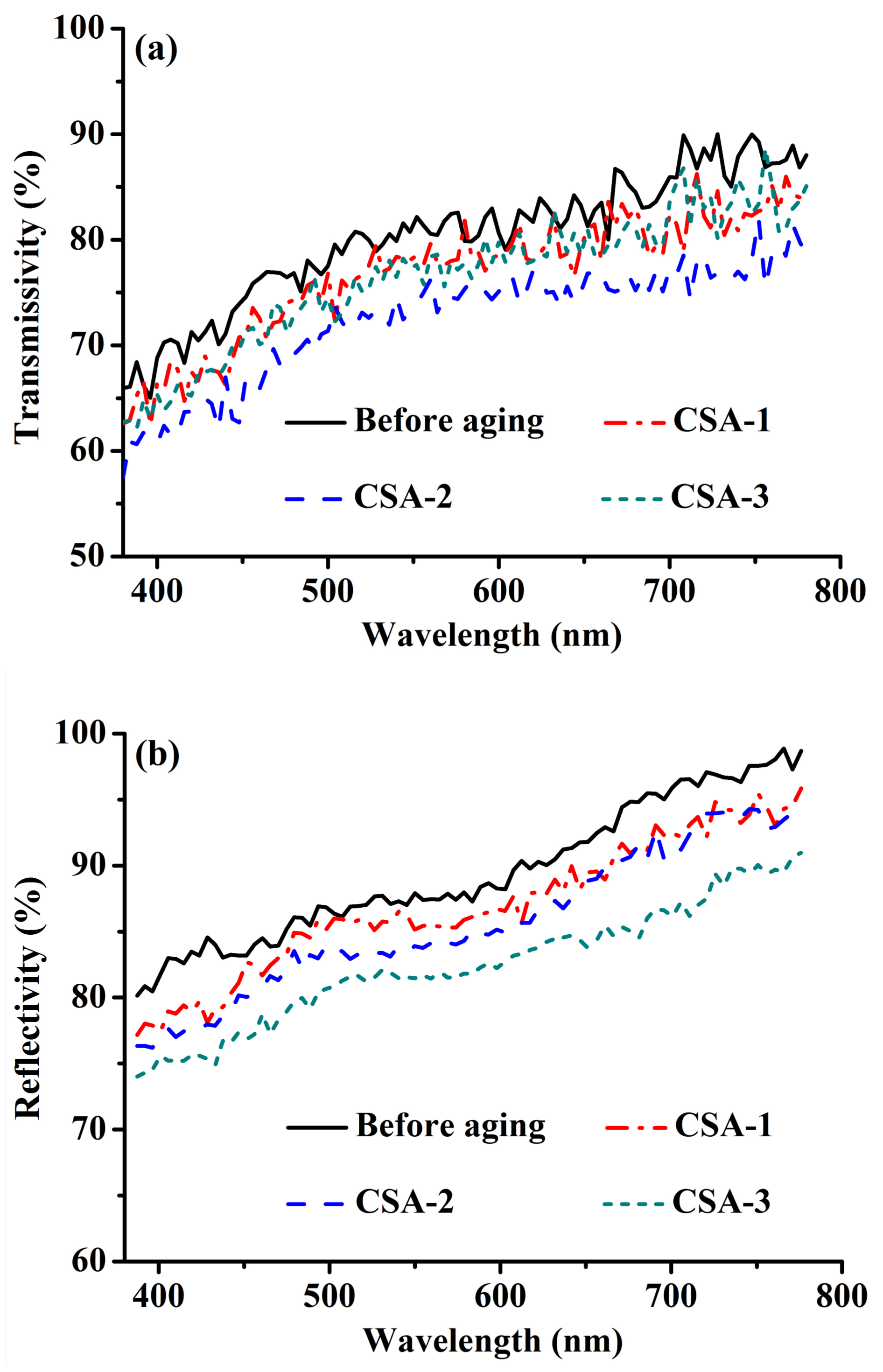
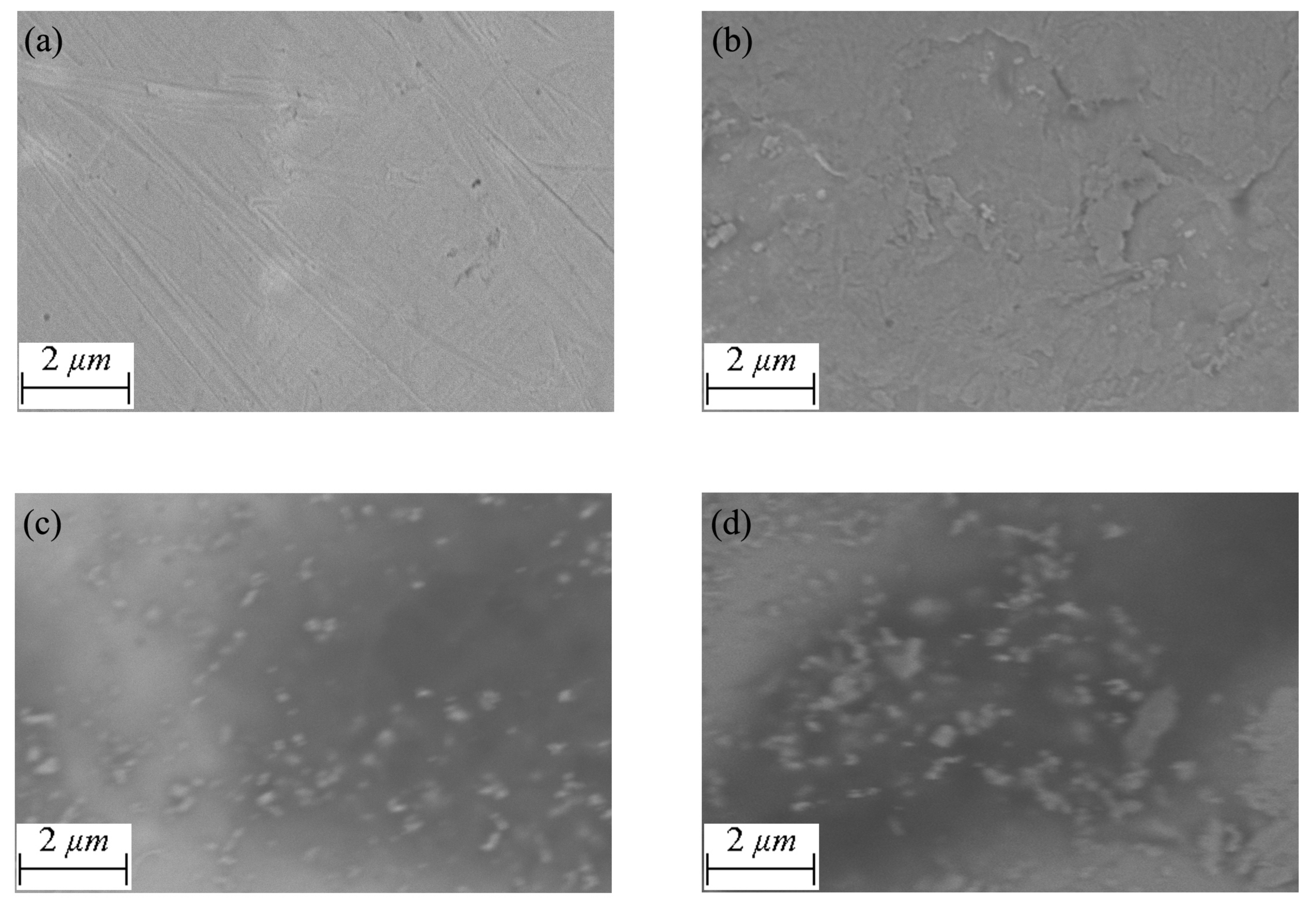
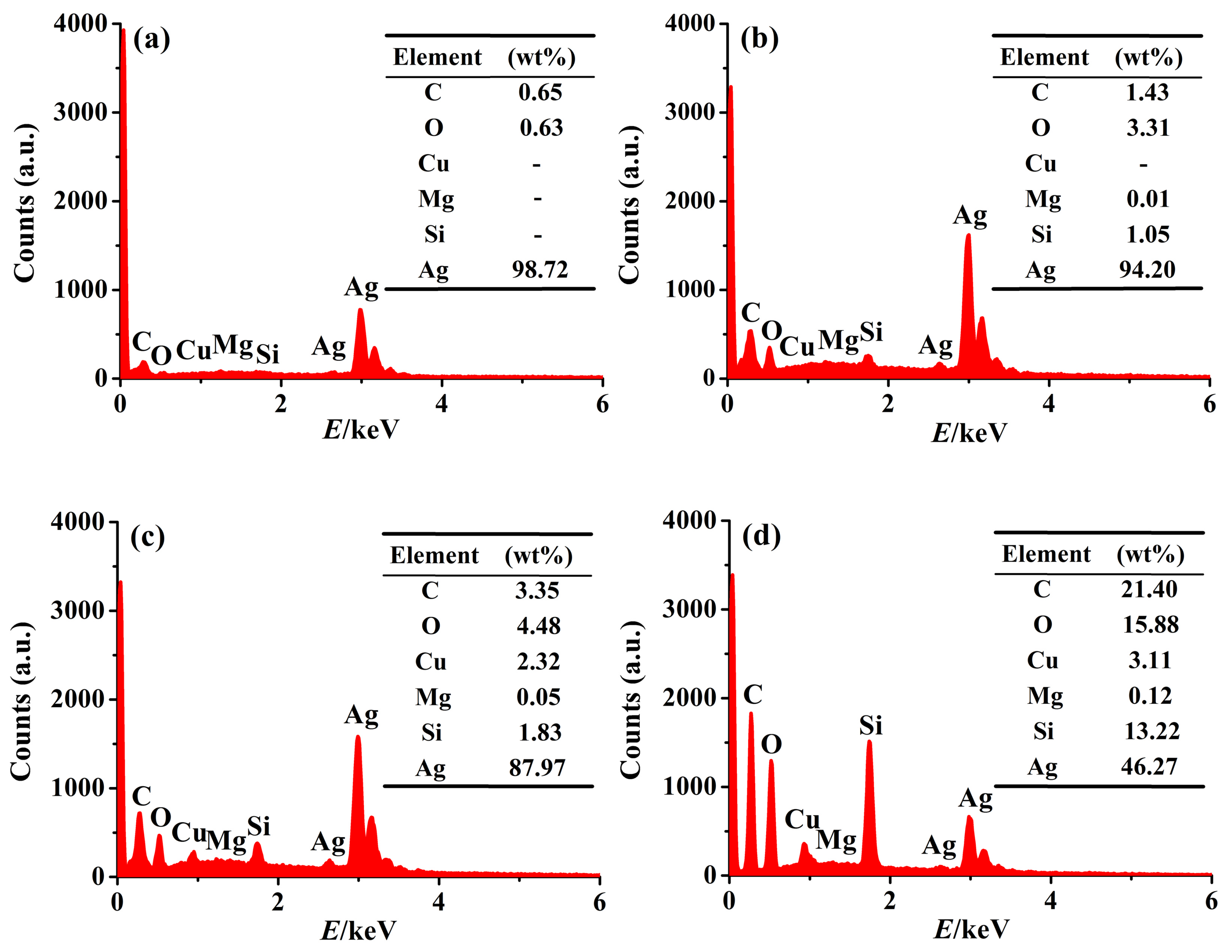
3.4. Packaging Analyses

Figure 8a depicts photographs of four representative samples corresponding to before and after aging for 3840 h in three cases, with sample number of analyzed samples as #6 (CSA-1), #16 (CSA-2), and #23 (CSA-3), respectively. Ratios of the optical power after 3840 h aging to the optical power before aging for #6, #16, and #23 are computed as 90.8%, 90.2%, and 80.7%, corresponding to 9.2%, 9.8%, and 19.3% optical decay, respectively. From the appearance in Figure 8a, the sample in CSA-2 exhibits remarkable yellow-browning in the optical lens, whereas that in CSA-3 demonstrates distinct darkening on the surface of the silver-coated reflective layer. Considering the optical decay and the surficial change, we rationalize that the darkening on the surface of the silver-coated reflective layer induces more serious degradation of the optical power than the yellow-browning in the silicone-based optical lens does.
Angular intensity distributions look like a pair of bat wings for peanut-shaped LEDs with maximum intensities at ±60 (Figure 8b). The largeness of view angles in these peanut-shaped LEDs clearly differs from that in conventional hemisphere-shaped LEDs [38]. Angles at which the maximum intensity occurs remain unchanged for all cases, whereas intensities in three aged cases display monotonic decreases at all tested angles as the current stress increases. These decreases may be attributed to the systematic degradation in hppc-WLEDs, including the yellow-browning of optical lenses, the darkening of silver-coated reflective layers, and the decomposition of phosphor-silicone mixtures.
We employ a white LED (with the current driven at 350 mA and the heat-sink temperature maintained at 25 C) to measure and compare transmissivities of silicone epoxy lenses and reflectivities of silver-coated reflective layers in an unaged device and three 3840 h-aged devices in CSA-1, CSA-2, and CSA-3, respectively. As shown in Figure 9a, all transmissivities of aged lenses experience a decrease in comparison with the unaged one at measured wavelengths ranging between 380 nm and 780 nm. Clearly, the transmissivity of the lens in CSA-2 lowers most severely among those of lenses in all aged cases. The reason for this loss lies in that the device in CSA-2 exhibits a prominent yellow-browning silicone epoxy lens. Besides, variations of reflectivities on surfaces of silver-coated reflective layers before and after aging are shown in Figure 9b. The reflectivity in CSA-3 is generally lower than those in CSA-1 and CSA-2 within the visible wavelength range due to the most severe darkening of the silver-coated reflective layer. Therefore, both decreases of the transmissivity of the silicone epoxy lens and the reflectivity of the silver-coated reflective layer are found to be strongly related to the optical power decays after aging.
To further investigate the degradation of silver-coated reflective layers, we employ a field emission scanning electron microscopy (FM-SEM) on surfaces of silver-coated reflective layers to observe microstructural changes of these surfaces before and after 3840 h aging, as shown in Figure 10. Results indicate that, in comparison with the surface of the un-aged sample (Figure 10a), dark areas are generated on those of aged silver-coated reflective layers (Figure 10b–d). Generally, the formation of dark areas can be primarily attributed to the carbonization effect of plastic encapsulation materials on surfaces of silver-coated reflective layers [39,40]. This effect reduces the intensity of the reflected light because the impinging light is absorbed by these dark areas. Compositional changes of silver-coated reflective layers have also been examined with an energy dispersive spectrometer (EDS). As shown in Figure 11a–d, some extra chemical elements, such as Cu, Mg, and Si, are found on surfaces of aged silver-coated reflective layers. By contrast, these elements are found absent on the unaged surface. Especially in CSA-3 (Figure 11d), the element C increases from 0.65 wt % to 21.40 wt %, and similarly, the element O increases from 0.63 wt % to 15.88 wt %. We deduce that increases of elements C and O can be associated with the degradation of silicone epoxy lenses. The element Si with 13.22 wt % in CSA-3 appears one order of magnitude higher than that with 1.05 wt % in CSA-1 and 1.83 wt % in CSA-2 only. Again, we conjecture that most of the element Si may deposit on surfaces of silver-coated reflective layers from phosphor-silicone mixtures. These significant increases of three elements can collectively demonstrate the highest degree of seriousness of the carbonization effect in CSA-3. In addition, small weight percentages of element Cu (CSA-1: none, CSA-2: 2.32 wt %, CSA-3: 3.11 wt %) and element Mg (CSA-1: 0.01 wt %, CSA-2: 0.05 wt %, CSA-3: 0.12 wt %) emerge on surfaces of aged silver-coated reflective layers. The emergence of the former stems from the exposure of the copper slug, whereas that of the latter stems from (a) the diffusion of the Mg dopant in p-GaN layer or/and (b) the cross-contamination during manufacturing and encapsulating processes of LEDs [41]. Conceivably, both elements Cu and Mg are highly correlated with high-current stresses.

4. Conclusions

We have investigated multiple degradation mechanisms of hppc-WLEDs under three current stresses (CSA-1, CSA-2, and CSA-3, respectively). Results indicate that the optical degradation is strongly correlated to the current stress. However, high current stresses do not necessarily cause severe optical decays. In the active layer of the LED chip, the Mg dopant reactivation and the annealing effect play positive roles in enhancing the optical power, whereas the increase of point defects plays a negative role in reducing the optical power. Packaging materials, such as silver-coated reflective layers, silicone epoxy lenses, and phosphor-silicone mixtures, degrade constantly when being subjected to the high-current stress. In addition, Ohmic contacts, thermal resistances, and angles of the maximum intensity remain unchanged, and contribute insignificantly to the degradation of LEDs during aging tests. Therefore, in this study, we have presented a comprehensive investigation of photometric, chromatic, electrical, thermal, and packaging analyses of hppc-WLEDs in current-stress aging processes. In practical applications, these experimental findings can provide LED communities with a guidance to develop reliable light sources.

Acknowledgments

This work was supported in parts by the International Science and Technology Cooperation Program of China (2015DFG62190), the Hong Kong, Macao, and Taiwan Special Science and Technology Cooperation Program (2015DFT10120), the National Natural Science Foundation of China (61504112, 11604285, and 51605404), the Science and Technology Project of the State Administration of Quality Supervision, Inspection and Quarantine (2014QK020), the Technological Innovation Project of Economic and Information Commission of Fujian Province, and the Strait Postdoctoral Foundation of Fujian Province.

Author Contributions

Hao-Chung Kuo and Zhong Chen proposed the main idea; Zhangbao Peng and Ziquan Guo performed all experiments and wrote the manuscript; Tingzhu Wu, Peng Zhuang, and Zhicheng Ye analyzed the data; Yuan Shi, Tien-Mo Shih, and Yijun Lu have contributed to the final revision.

Conflicts of Interest

The authors declare no conflict of interest.

References

  1. May, B.J.; Selcu, C.M.; Sarwar, A.T.M.G.; Myers, R.C. Nanoscale current uniformity and injection efficiency of nanowire light emitting diodes. Appl. Phys. Lett. 2018, 112, 093107. [Google Scholar] [CrossRef]
  2. Tsai, H.; Nie, W.; Blancon, J.C.; Stoumpos, C.C.; Soe, C.M.M.; Yoo, J.; Crochet, J.; Tretiak, S.; Even, J.; Sadhanala, A.; et al. Stable light-emitting diodes using phase-pure ruddlesden-popper layered perovskites. Adv. Mater. 2018, 30, 1704217. [Google Scholar] [CrossRef] [PubMed]
  3. Lin, H.Y.; Chen, K.J.; Wang, S.W.; Lin, C.C.; Wang, K.Y.; Li, J.R.; Lee, P.T.; Shih, M.H.; Li, X.L.; Chen, H.M.; et al. Improvement of light quality by DBR structure in white LED. Opt. Express 2015, 23, 27–33. [Google Scholar] [CrossRef] [PubMed]
  4. Guo, Z.Q.; Shih, T.M.; Lu, Y.J.; Gao, Y.L.; Zhu, L.H.; Chen, G.L.; Zhang, J.H.; Lin, S.Q.; Chen, Z. Studies of scotopic/photopic ratios for color-tunable white light-emitting diodes. IEEE Photonics J. 2013, 5, 8200409. [Google Scholar] [CrossRef]
  5. Kim, G.; Sun, M.C.; Kim, J.H.; Park, E.; Park, B.G. GaN-based light emitting diodes using p-type trench structure for improving internal quantum efficiency. Appl. Phys. Lett. 2017, 110, 021115. [Google Scholar] [CrossRef]
  6. Tsai, Y.L.; Liu, C.Y.; Krishnan, C.; Lin, D.W.; Chu, Y.C.; Chen, T.P.; Shen, T.L.; Kao, T.S.; Charlton, M.D.B.; Yu, P.; et al. Bridging the “green gap” of LEDs: Giant light output enhancement and directional control of LEDs via embedded nano-void photonic crystals. Nanoscale 2016, 8, 1192–1199. [Google Scholar] [CrossRef] [PubMed]
  7. Fadil, A.; Ou, Y.Y.; Iida, D.; Kamiyama, S.; Petersen, P.M.; Ou, H.Y. Combining surface plasmonic and light extraction enhancement on InGaN quantum-well light-emitters. Nanoscale 2016, 8, 16340–16348. [Google Scholar] [CrossRef] [PubMed]
  8. Wu, P.C.; Ou, S.L.; Horng, R.H.; Wuu, D.S. Improved performance of high-voltage vertical GaN LEDs via modification of micro-cell geometry. Appl. Sci. 2017, 7, 506. [Google Scholar] [CrossRef]
  9. Kim, T.; Seong, T.Y.; Kwon, O. Investigating the origin of efficiency droop by profiling the voltage across the multi-quantum well of an operating light-emitting diode. Appl. Phys. Lett. 2017, 108, 231101. [Google Scholar] [CrossRef]
  10. Guo, Z.Q.; Shih, T.M.; Gao, Y.L.; Lu, Y.J.; Zhu, L.H.; Chen, G.L.; Lin, Y.; Zhang, J.H.; Chen, Z. Optimization studies of two-phosphor-coated white light-emitting diodes. IEEE Photonics J. 2013, 5, 8200112. [Google Scholar] [CrossRef]
  11. Shen, W.Q.; Zhu, Y.W.; Wang, Z.L. Luminescent properties of Sr4Si3O8Cl4:Eu2+, Bi3+ phosphors for near UV InGaN-based light-emitting-diodes. Appl. Sci. 2015, 5, 1494–1502. [Google Scholar] [CrossRef]
  12. Meneghini, M.; Lago, M.D.; Trivellin, N.; Meneghesso, G.; Zanoni, E. Degradation mechanisms of high-power LEDs for lighting applications: An overview. IEEE Trans. Ind. Appl. 2014, 50, 78–85. [Google Scholar] [CrossRef]
  13. Renso, N.; Meneghini, M.; Buffolo, M.; Santi, C.D.; Meneghesso, G.; Zsnoni, E. Understanding the degradation processes of GaN based LEDs submitted to extremely high current density. Microelectron. Reliab. 2017, 76–77, 556–560. [Google Scholar] [CrossRef]
  14. Singh, P.; Tan, C.M. Degradation physics of high power LEDs in outdoor environment and the role of phosphor in the degradation process. Sci. Rep. 2016, 6, 24052. [Google Scholar] [CrossRef] [PubMed]
  15. Ruknudeen, F.; Asokan, S. Application of particle filter to on-board life estimation of LED lights. IEEE Photonics J. 2017, 9, 8201116. [Google Scholar] [CrossRef]
  16. Rahman, F.; George, A.F.; Drinkard, R. Short- and long-term reliability studies of broadband phosphor-converted red, green, and white light-emitting diodes. IEEE Trans. Device Mater. Rel. 2016, 16, 1–8. [Google Scholar] [CrossRef]
  17. Canale, L.; Dupuis, P.; Leng, S.; Zissis, G. Study of high-brightness LED samples aged under stress temperature conditions: Electrical characterizations and signature evolution analysis. IEEE Trans. Ind. Appl. 2016, 52, 502–510. [Google Scholar] [CrossRef]
  18. Fan, J.J.; Yu, C.H.; Qian, C.; Fan, X.J.; Zhang, G.Q. Thermal/luminescence characterization and degradation mechanism analysis on phosphor-converted white LED chip scale packages. Microelectron. Reliab. 2017, 74, 179–185. [Google Scholar] [CrossRef]
  19. Joglekar, S.; Azize, M.; Beeler, M.; Monroy, E.; Palacios, T. Impact of recess etching and surface treatments on ohmic contacts regrown by molecular-beam epitaxy for AlGaN/GaN high electron mobility transistors. Appl. Phys. Lett. 2016, 74, 041602. [Google Scholar] [CrossRef]
  20. Vaskuri, A.; Kärhä, P.; Baumgartner, H.; Kantamaa, O.; Pulli, T.; Poikonen, T.; Ikonen, E. Relationships between junction temperature, electroluminescence spectrum and ageing of light-emitting diodes. Metrologia 2018, 55, S86–S95. [Google Scholar] [CrossRef]
  21. Iqbal, F.; Kim, S.; Yie, H.Y.; Kim, Y.; Kim, H. Effect of alkali metal oxides on reliability and degradation of phosphor-in-glass encapsulants for white LEDs. Ceram. Int. 2016, 42, 10393–10398. [Google Scholar] [CrossRef]
  22. Neugebauer, S.; Hoffmann, M.P.; Witte, H.; Bläsing, J.; Dadgar, A.; Strittmatter, A.; Niermann, T.; Narodovitch, M.; Lehmann, M. All metalorganic chemical vapor phase epitaxy of p/n-GaN tunnel junction for blue light emitting diode applications. Appl. Phys. Lett. 2017, 110, 102104. [Google Scholar] [CrossRef]
  23. Lee, D.H.; Mitchell, B.; Fujiwara, Y.; Dierolf, V. Thermodynamics and kinetics of three Mg-H-VN complexes in Mg:GaN from combined first-principles calculation and experiment. Phys. Rev. Lett. 2014, 112, 205501. [Google Scholar] [CrossRef]
  24. Luo, X.B.; Hu, R.; Liu, S.; Wang, K. Heat and fluid flow in high-power LED packaging and applications. Prog. Energ. Combust. 2016, 56, 1–32. [Google Scholar] [CrossRef]
  25. Liu, L.L.; Yang, J.F.; Ling, M.J.; Zhong, J.W.; Teng, D.D.; Wang, G. Aggravated efficiency droop in vertical-structured gallium nitride light-emitting diodes induced by high temperature aging. J. Appl. Phys. 2013, 113, 083105. [Google Scholar] [CrossRef]
  26. Shimizu, K.T.; Böhmer, M.; Estrada, D.; Gangwal, S.; Grabowski, S.; Bechtel, H.; Kang, E.; Vampola, K.J.; Chamberlin, D.; Shchekin, O.B.; et al. Toward commercial realization of quantum dot based white light-emitting diodes for general illumination. Photonics Res. 2017, 5, A1–A6. [Google Scholar] [CrossRef]
  27. Yang, T.H.; Wu, S.M.; Sun, C.C.; Glorieux, B.; Chen, C.Y.; Chang, Y.Y.; Lee, X.H.; Yu, Y.W.; Chung, T.Y.; Lai, K.Y. Stabilizing CCT in pcW-LEDs by self-compensation between excitation efficiency and conversion efficiency of phosphors. Opt. Express 2017, 25, 29287–29295. [Google Scholar] [CrossRef]
  28. Cai, M.; Yang, D.G.; Huang, J.L.; Zhang, M.F.; Chen, X.P.; Liang, C.H.; Koh, S.; Zhang, G.Q. Color shift modeling of light-emitting diode lamps in step-loaded stress testing. IEEE Photonics J. 2017, 9, 8200114. [Google Scholar] [CrossRef]
  29. Borga, M.; Meneghini, M.; Rossetto, I.; Stoffels, S.; Posthuma, N.; Hove, M.V.; Marcon, D.; Decoutere, S.; Meneghesso, G.; Zanoni, E. Evidence of time-dependent vertical breakdown in GaN-on-Si HEMTs. IEEE Trans. Electron Dev. 2017, 64, 3616–3621. [Google Scholar] [CrossRef]
  30. Haller, C.; Carlin, J.F.; Jacopin, G.; Martin, D.; Butté, R.; Grandjean, N. Burying non-radiative defects in InGaN underlayer to increase InGaN/GaN quantum well efficiency. Appl. Phys. Lett. 2017, 111, 262101. [Google Scholar] [CrossRef]
  31. Ajia, I.A.; Edwards, P.R.; Pak, Y.; Belekov, E.; Roldan, M.A.; Wei, N.; Liu, Z.Q.; Martin, R.W.; Roqan, I.S. Generated carrier dynamics in V-pit-enhanced InGaN/GaN light-mitting diode. ACS Photonics 2018, 5, 820–826. [Google Scholar] [CrossRef]
  32. Bicanic, K.T.; Li, X.Y.; Sabatini, R.P.; Hossain, N.; Wang, C.F.; Fan, F.J.; Liang, H.Y.; Hoogland, S.; Sargent, E.H. Design of phosphor white light systems for high-power applications. ACS Photonics 2016, 3, 2243–2248. [Google Scholar] [CrossRef]
  33. Monti, D.; Meneghini, M.; Santi, C.D.; Meneghesso, G.; Zanoni, E. Degradation of UVA LEDs: Physical origin and dependence on stress conditions. IEEE Trans. Device Mater. Rel. 2016, 16, 213–218. [Google Scholar] [CrossRef]
  34. Spencer, P.; Clarke, E.; Murray, R. Carrier escape and the ideality factor in quantum dot p-n junctions. IEEE J. Quantum Elect. 2014, 50, 213–219. [Google Scholar] [CrossRef]
  35. Pfeiffer, L.N.; West, K.W. Quantum hall spin diode. Phys. Rev. Lett. 2017, 118, 186801. [Google Scholar] [CrossRef]
  36. Su, C.Y.; Tu, C.G.; Liu, W.H.; Lin, C.H.; Yao, Y.F.; Chen, H.T.; Wu, Y.R.; Kiang, Y.W.; Yang, C.C. Enhancing the hole-injection efficiency of a light-emitting diode by increasing Mg doping in the p-AlGaN electron-blocking layer. IEEE Trans. Electron Dev. 2017, 64, 3226–3233. [Google Scholar] [CrossRef]
  37. Chen, T.T.; Wang, C.P.; Fu, H.K.; Chou, P.T.; Ying, S.P. Electroluminescence enhancement in InGaN light-emitting diode during the electrical stressing process. Opt. Express 2014, 22, 1328–1333. [Google Scholar] [CrossRef] [PubMed]
  38. Yu, S.D.; Li, Z.T.; Liang, G.W.; Tang, Y.; Yu, B.H.; Chen, K.H. Angular color uniformity enhancement of white light-emitting diodes by remote micro-patterned phosphor film. Opt. Lett. 2016, 4, 140–145. [Google Scholar] [CrossRef]
  39. Tsai, M.Y.; Tang, C.Y.; Wang, C.H.; Tsai, Y.Y.; Chen, C.H. Investigation on some parameters affecting optical degradation of LED packages during high-temperature aging. IEEE Trans. Device Mater. Rel. 2015, 15, 335–341. [Google Scholar] [CrossRef]
  40. Jung, E.J.; Kim, M.S.; Kim, H. Analysis of contributing factors for determining the reliability characteristics of GaN-based white light-emitting diodes with dual degradation kinetics. IEEE Trans. Electron Dev. 2013, 60, 186–191. [Google Scholar] [CrossRef]
  41. Lu, Y.J.; Guo, Z.Q.; Shih, T.M.; Gao, Y.L.; Huang, W.L.; Lu, H.L.; Lin, Y.; Chen, Z. Optical degradation mechanisms of indium gallium nitride-based white light emitting diodes by high-temperature aging tests. IEEE Trans. Rel. 2016, 65, 256–262. [Google Scholar] [CrossRef]
Figure 1. The schematic structure of peanut-shaped hppc-WLEDs.
Applsci 08 00610 g001
Figure 2. The normalized optical power versus aging time in three cases.
Applsci 08 00610 g002
Figure 3. (a) The CCT variation versus aging time in three cases; SPDsof representative samples for three cases: (b) CSA-1; (c) CSA-2; and (d) CSA-3, respectively, prior to and after aging.
Applsci 08 00610 g003
Figure 4. The I-V curves of representative hppc-WLEDs before and after 3840 h aging in cases of (a) CSA-1; (b) CSA-2; and (c) CSA-3, respectively; (d) Optical decays at various currents in three cases.
Applsci 08 00610 g004
Figure 5. The forward voltage versus aging time in three cases.
Applsci 08 00610 g005
Figure 6. For the case of CSA-2: the normalized optical power versus aging time (black square, left vertical axis) and the ideality factor versus aging time (red circle, right vertical axis) with respective error bars.
Applsci 08 00610 g006
Figure 7. (a) The cumulative structure function of samples; and those of samples before and after 3840 h aging in cases of (b) CSA-1; (c) CSA-2; and (d) CSA-3, respectively.
Applsci 08 00610 g007
Figure 8. (a) Photographs of four representative samples; and (b) angular intensity distributions of hppc-WLEDs.
Applsci 08 00610 g008
Figure 9. Before and after 3840 h aging in CSA-1, CSA-2, and CSA-3, respectively: (a) transmissivities of silicone epoxy lenses; and (b) reflectivities of silver-coated reflective layers.
Applsci 08 00610 g009
Figure 10. The SEMimages on surfaces of silver-coated reflective layers: (a) one unaged sample; and three representative aged samples in (b) CSA-1; (c) CSA-2; and (d) CSA-3, respectively (after 3840 h aging).
Applsci 08 00610 g010
Figure 11. The EDS chemical element contents on surfaces of silver-coated reflective layers: (a) one unaged sample, and three representative aged samples in (b) CSA-1; (c) CSA-2; and (d) CSA-3; respectively (after 3840 h aging).
Applsci 08 00610 g011
Table 1. Various items and their characteristics of instruments used in the experimental study.
InstrumentModelCharacteristic
SpectrometerSpectro-320eWavelength: 170–1700 nm
Integrating SphereISP-500, ISP-150Sizes: 500 mm, 150 mm
Angular Distribution AnalyzerLEDGON 100Angle range: 360 ; Angle accuracy: 1
Transient Thermal Tester (T3Ster)T3Ster 2000/100Testing currents: 0–500 mA; Resolution: 0.1 C
Electric Source MeterKeithley 2611Maximum current: 1.5 A; Maximum voltage: 200 V
Temperature ControllerKeithley 2510Temperature range: 0–80 C; Resolution: 0.001 C
Field emission Scanning Electron Microscopy (FE-SEM)Sigma-HDMagnifications: 10–1,000,000×; Resolution: 1.0 nm
Energy Dispersive Spectrometer (EDS)X-Max N SDD detector: 50 mm 2 ; Accuracy: 5 nm

