1. Introduction
This is well known that thin (no thicker than a few tens of nanometers) metal layers sandwiched between two dielectrics having the same refraction indices (RI) support the propagation of long-range surface plasmon polaritons (LRSPP) appearing as a result of the interference of SPP pertinent to the two neighboring metal-dielectric interfaces [
1,
2,
3]. (For brevity, below we will usually omit the word polariton speaking simply about surface plasmons). Besides fundamental researches, during previous years this effect has been used also for sensing purposes, somewhat analogously (but with certain advantages caused by the long propagation distances in the case) to more standard surface plasmon resonance (SPR)-based sensors (see e.g., [
4,
5] for general reviews of the field). Both (almost) free-standing thin metal layers, and such layers working in water and deposited onto an appropriate substratum made from material having the same RI as the water (e.g., particular Teflon) were exploited [
6,
7]. However, certainly, the necessity to construct a symmetric “sandwich” structure to support the LRSPP propagation poses a serious problem to be overcome and limits further development of the method. This is true even when the exploitation of such an approach in water is at stake (water’s relatively low refraction index
n = 1.33 drastically limits the choice of appropriate supports) and makes the work almost impossible in gases is their RI is very close to unity.
The situation has changed completely when it was recognized that somewhat similar situation occurs when one of the dielectrics of a symmetrical sandwich structure is replaced with a specially designed Photonic Crystal (PC) [
8]. This enabled the launch and use of surface plasmons (in the red spectral region) for such “non-plasmonic” materials as palladium [
9,
10,
11] and cobalt [
12], as well as launch and use blue (at 405 nm [
13]) surface plasmons for gold. Note, that in all of the above cases, without the properly designed Photonic Crystal supporting LRSPP, there is simply no point in speaking about surface plasmons at all: their propagation distances would then be just of the order of the wavelength.
Another big topic is the use of PC-supported surface electromagnetic waves without any metal layer, which has numerous implications in sensorics, electromagnetic field control at the surface and so forth. This topic is relatively far from the research under discussion now, but for completeness, we still would like to indicate a few corresponding essential papers and reviews [
14,
15,
16,
17,
18,
19,
20,
21,
22], see further references therein.
In this paper, we report on the realization of PC-supported long-range surface plasmons for silver at the red wavelength of He-Ne laser, λ = 632.8 nm. Quite narrow plasmon resonances, attesting to the ultralong SPP propagation and high quality of silver films, were observed. From one point of view, silver is always considered as the best surface plasmon-supporting metal in the red and near-infrared spectral ranges. However, from another point of view, the difficulties in the preparation of high-quality thin layers of silver and rapid degradation of this material exposed to the atmosphere make its exploitation quite tricky. To the best of our knowledge, up to date LRSPP with thin silver nanofilms have been realized only with the (almost) symmetrical sandwich structures composed of silica and (very) thick layers of an index matching oil or polymer [
23,
24], so that their exploitation as sensors seems not possible.
We also profit a lot from the extensive experience of preparation of thin silver layers onto different dielectrics gained by the Australian team, especially in the course of the researches aiming at the optimization of thin film coatings for solar and thermal radiation control, see e.g., [
25,
26]. Important peculiarity here is the use of materials, which are not oxide materials, as adjacent layers for silver. Detailed discussion of this point is given in the next Section.
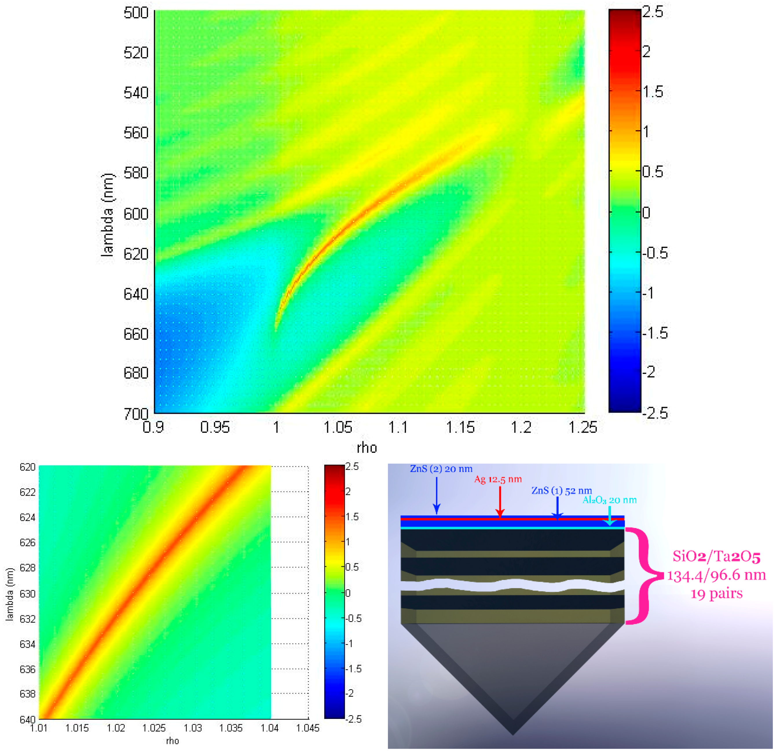
2. Photon Crystal Design
The following structure (see
Figure 1) has been designed and prepared to realize LRSPP propagation along silver-ZnS/air interface: SiO
2/(HL)
19/Al
2O
3/ZnS(1)/Ag/ZnS(2)/air, where SiO
2 are standard 2.3 mm thick fused silica plate, (HL)
19 are 19 pairs of tantalum pentoxide and silicon dioxide layers (that is transparent dielectrics having high and low refraction indices which form a 1D Photonic Crystal) with the thicknesses respectively 96.6 and 134.4 nm, Al
2O
3 layer has a thickness of 20 nm, ZnS layers 1 and 2 have the thicknesses respectively 52 and 20 nm, Ag is 12.5 nm-thick silver layer. SiO
2/(HL)
19 Photonic Crystal on silica substrate has been prepared by magnetron sputtering in one coating run, and afterward all other layers have been deposited on top of this finished structure also in one (but another) coating run.
In the Introduction, we already mentioned the usefulness of the exploitation of non-oxide materials together with metal nanofilms [
25,
26]. (Shortcomings related with the use of broadly accepted oxide materials for such purposes, e.g., an easy oxidation of ultrathin metal layers, strong tendency of such layers to form nanoparticle islands or agglomerates in the absence of any special “wetting layers” or the like, are discussed in the same references and elsewhere). Through extensive experimentation with ultrathin (sub-15 nm) Ag layers deposited by either thermal evaporation or sputtering, we have found that one possible solution to improve the thin layer morphology (preventing island-type growth) was to carefully select the underlying layer chemistry, and established that ZnS sublayers (substrate layers for Ag) led consistently to improving the layer morphology. In particular, the near IR reflection/transmission (R/T) spectra of custom-designed low-emissivity multilayer coatings employing them have been systematically studied. It is well-known that when the morphology of layers is compromised (island growth with holes in-between takes place), this unavoidably leads to the insufficient reflection of near-IR light by these layers and the coatings based on them. Only if the R/T spectra of multilayer coatings employing at least two Ag layers of thickness below 15 nm are fitted very closely with the spectra predicted using the data pertinent for idealized Ag layers (bulk
n and
k data), we could conclude that the morphology of growth is close to an ideal one. Exactly such a situation takes place in practice, which allows us to claim the quality of ultrathin silver layers when ZnS substrate layer was used. A thickness of 12.5 nm for the silver layer has been selected as the minimal thickness for which, according to our experience, high-quality of the film is achieved.
For the principles of optimal PC design see [
27]. The thicknesses of H and L layers forming PC were selected following the procedure optimizing the extinction per unit length (for a given wavelength and external media, of course), the thickness of the ZnS(2) layer of
dZnS2 = 20 nm was selected as “the smallest sufficient” to protect the silver layer from atmosphere. Al
2O
3 layer (of again the smallest reasonable thickness) was used to improve the quality and adhesion of the first ZnS(1) layer. Finally, we optimize the thickness of this same first internal ZnS(1) layer to achieve the most favorable conditions for LRSPP propagation, and optimize the number of pairs of layers in PC to have the maximal amplification of the light wave on the silver-ZnS interface.
An essential difference of the structure at hand in comparison with the earlier used PC supporting LRSPP propagation [
8,
9,
10,
11,
13] is the appearance of one additional protective ZnS(2) layer which necessitates the following modifications. In impedance representation [
27], the condition for the surface wave propagation remains the same:
Zleft +
Zright = 0, where
Zleft is an impedance of the system SiO
2/(HL)
19/Al
2O
3/ZnS(1)/Ag calculated using recursion formulae of Ref. [
27] together with the formula (13) describing impedance of the photonic crystal there (for current purposes we can consider this PC as an infinite one). However, now
Zright is
not an impedance of the infinite external media (air) equal to
but instead an impedance of the system ZnS(2)/air which is equal to
where
,
, and
is a “propagation parameter”, viz., an angular variable equal to
. This variable, according to the Snell’s law, remains the same for each layer having the refraction index
ni with
being an angle between the propagating light and the normal to all interfaces [
27]. This change is not negligible and must be taken into account because already for 20 nm-thick ZnS layer with the refraction index
nZnS = 2.318 and
we have comparable values of
αZnS2 = 0.41,
Zair = 0.1285
i and
ZZnS= 0.39. At the same time, for many practical purposes, the whole effect of this additional layer can be seen simply as a relatively slight modification of the refraction index of an infinite external medium. Comparing (1) and (2) we see that for
Equation (1) gives the same impedance as Equation (2) if one put
nair =
neff = 1.03 into Equation (1).
The results of our calculations are presented in
Figure 1. It is easy to see that for He-Ne laser wavelength of 632.8 nm we do have a LRSPP wave characterized by the angular variable (propagation parameter)
and possessing quite strong thirty-fold enhancement of the intensity of light.
3. Experimental Results and Discussion
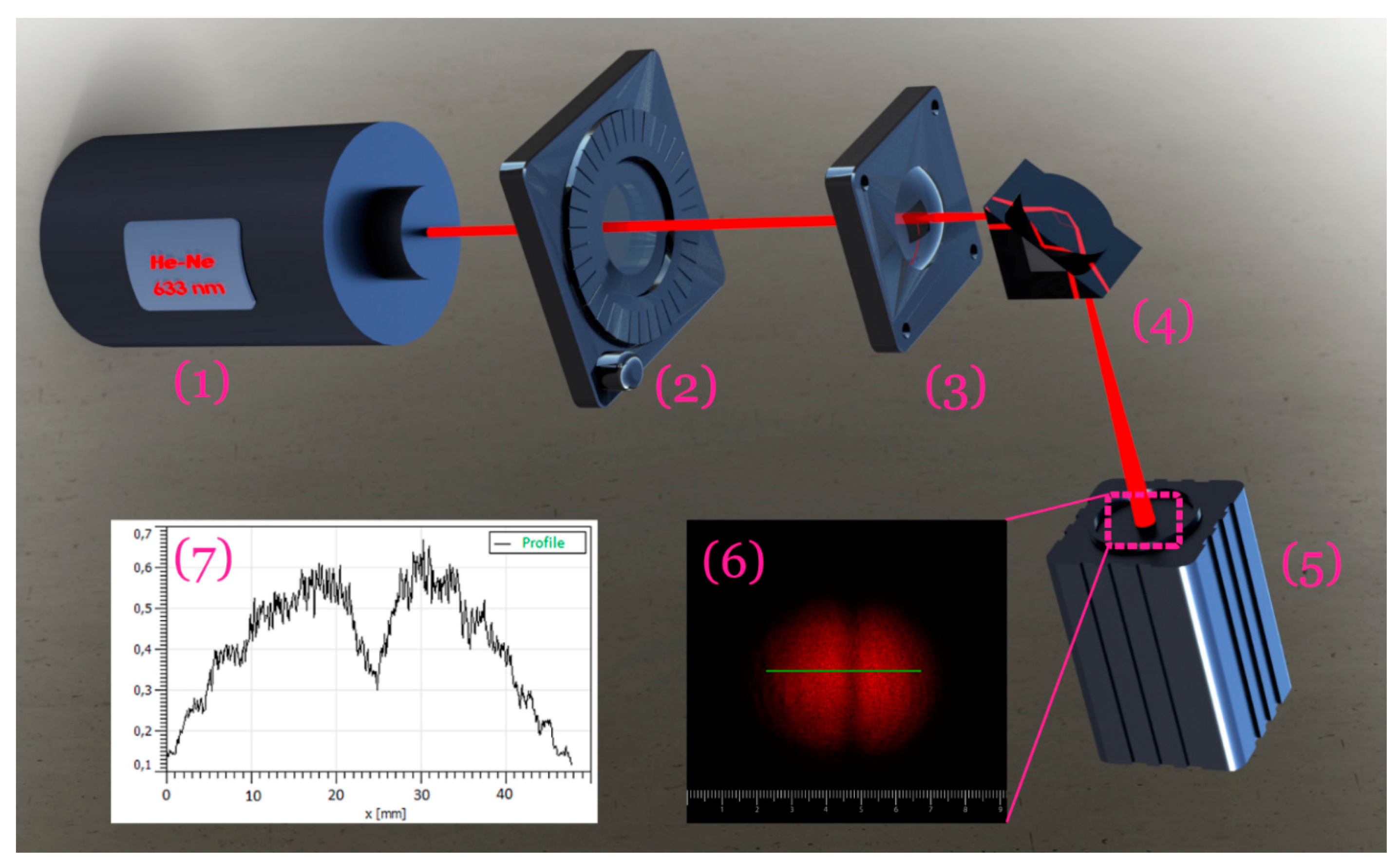
Schematic of an experimental setup together with the data attesting an observation of very narrow angular plasmon resonance in the light reflection from the aforementioned PC + Ag layer structure are presented in
Figure 2. For the measurements of LRSPP, standard Kretschmann configuration employing quartz 45
0 prism on which the structure at question has been “glued” via a droplet of phase matching oil has been used [
28]. Standard p-polarized He-Ne laser light (beam diameter around 5 mm) has been focused on the structure studied with 10 cm focal length lens, and the angular structure of the reflected light has been recorded observing the light spots at distances of 162 and/or 405 cm (both recordings of the light intensity with CMOS (complementary metal-oxide semiconductor) camera and processing of color digital photographs of the corresponding light spots were used leading to essentially the same results).
Surface plasmon excitation has been observed for conditions quite close to the normal incidence of the incoming light beam onto the prism entrance face: the corresponding angle was equal to 0.3° which results in the incidence angle onto the prism hypotenuse giving the propagation parameter . Deviation of this value from the theoretical one is due to the deviations of actual refraction indices and layer thicknesses from the (theoretical or “searched for”) values used in calculations, and this is quite common for the field.
Another indication of the narrowness of the plasmon resonance in our structure has been obtained when we, in the same configuration, used unfocused He-Ne laser beam: for an optimal adjustment, the intensity of reflected light dropped from 5.9 mW (out of resonance) to 2.6 mW (in resonance) thus attesting that more than one half of an incoming radiation power has been transferred into the surface wave. The same experiment also was used to demonstrate the polarization dependence of the observed reflection minimum: the difference in the intensity of light reflected for out of- and in-resonance conditions well followed the content of the p-polarized light in the incoming laser beam (it was changed by the rotation of He-Ne laser having the polarization ratio not smaller than 50:1 without a polarizer), and such a difference was completely undetectable for the pure s-polarization case.
The width of the angular resonance curve in
Figure 2 is equal to ca.
which corresponds to the surface plasmon propagation length
l of approximately 180 microns. (Standard formula
was used. Here, the subscript
pr corresponds to the values inside the prism; the value of
can be recalculated from the experimentally measured
by applying Snell’s law. For our case of almost normal incidence of light onto the prism catet
). Comparable, but slightly worse results with the angular width somewhat exceeding 10
−3 rad were obtained when using a semiconductor cw fiber Bragg grating laser diode at the wavelength of 636.7 nm (QPhotonics LLC, Ann Arbor, MI, USA). This is the main result of our research, and it unambiguously attests the first realization of LRSPP for PC-supported silver nanofilms. The long-term stability of the prepared structures was noticed: the reflection parameters remained virtually the same during nine months of observations; the sample has been kept in usual room conditions in a polyethylene packet (not hermetically sealed).
The experimentally observed value
enables to determine the actual distribution of the square
(EE*) of electric field of SPP both inside an external medium (air, for which we take the refraction index equal to unity) and PC. For the former, we have an exponential decrease with the characteristic length
, that is much larger than the thickness of the ZnS layer adjacent to the silver nanofilm. Inside the Photonic Crystal, we have a standing wave with an exponentially decreasing envelope
eKz. The value of
K can be found applying e.g., Formulae (2) of [
8]. An easy calculation gives
which corresponds, for the PC period
= 231 nm, to the characteristic decay length of
. (Actually, the same value can be obtained calculating the transmission coefficient for one period of PC, see Section 2.4 of [
27]). The precise field distribution inside a metal layer and, correspondingly, inside the dielectric layers immediately adjacent to it, is quite sensitive to the exact thickness of metal layer and its refraction index which define the location of the minimum of an electric field inside the nanofilm, see a detailed discussion in [
8,
27]. This question is not relevant for the present work and has not been specially studied.
Discussing the obtained results, we first want to note that the observed LRSPP propagation length in our silver nanofilm-based structures is quite comparable to the value of 160 microns reported in [
8] for LRSPP supported by a specially designed PC and ca. 5 nm—thick gold film at the wavelength of 710 nm. This is not surprising given the quite comparable “plasmonic qualities” of gold and silver at the (different) wavelengths at question: according to Palik’s book [
29], at 710 nm we have
which gives
for the quantity describing the dissipation for SPP propagating along the interface air—infinitely thick gold layer [
28]. For our case, using the experimentally measured (by our group) value of the silver refraction index for a given wavelength,
nAg = 0.1345 + 3.986
i, that is
= −15.8701 + 1.0722
i, we have
. However, one should also note more than two times smaller value of the metal layer thickness, ca. 5 nm, in experiments reported in [
8]: a very important factor, given the inverse quadratic dependence of the LRSPP dissipation on this same thickness [
1,
2,
3]. All this, again, should be considered as the demonstration of truly high-quality silver nanofilm in our case.
Indeed, comparable LRSPP propagation lengths have been observed also in experiments with Pd [
10] and Co [
12] nanofilms deposited onto the properly designed PC. The common characteristic feature here is that in all of these cases, the experimentally measured values, although are impressively large enough and much exceed the propagation lengths for simple metal—dielectric interfaces, turn out to be substantially smaller than those which could be achieved according to the theoretical predictions.
The latter can be estimated approximating the real system by a “symmetrical sandwich structure composed by an infinite medium with the refraction index
neff—thin, with the thickness
dm, metal layer with the refraction index
nm—an infinite medium with the refraction index
neff”, using the value
neff = 1.03 described above (varying of this value contributes to the result quite slightly). In the so called Leontovich approximation, see formula A3 from Konopsky paper [
27] and other details therein, we have:
As a function of , this is simple biquadratic equation
where
, and its solution gives us
corresponding to the theoretical propagation length of
, which is two orders of magnitude larger than the experimentally measured value. Similarly, for gold at 710 nm and for the thickness of 5 nm, cf. [
8], we have
, for palladium at 739 nm with
d = 8 nm and
nPd = 1.9 + 4.8
i [
10,
27] we have
, and so forth.
Certainly, for the case of nanofilms, additional damping mechanisms exist and should be taken into account. The most well-known and fundamental one is the collision-induced scattering of conducting electrons at the walls of the nanofilm (“anomalous skin- and size-effects”) which has been profoundly discussed starting from the end of the forties (see e.g., [
30,
31] and references therein; see also [
27]). For our purposes, it is sufficient to present here only the final formula pertinent for the imaginary part of the dielectric constant for a continuous thin film at a frequency
[
30]:
where
d is nanofilm thickness,
is plasma frequency,
—Fermi velocity and
p—the so called “scattering parameter” defined as a fraction of electrons specularly reflected on the walls. (Real part of the dielectric constant is practically non-affected by this same scattering). For a completely diffuse scattering,
p = 0, Formula (5) gives the following limit for small thicknesses:
Taking for estimations for our case of silver nanofilm
m/s [
32],
= 9 eV [
33],
d = 12.5 nm and the frequency corresponding to the He-Ne laser used, we have
. This is non-negligible but still not such a significant change given that
, and it results in the new value of an effective refractive index of the “gold in the nanofilm”
. Substitution of this value into formula (4) instead of
nAg = 0.1345 + 3.986
i leads only to a minor change in the dissipation giving
The same conclusion can be drawn applying formula (6) for other cases, such as gold and palladium.
This same aforementioned noticeable difference between the experimentally observed and theoretically possible propagation lengths of LRSPP supported by Photonic Crystals should not be considered as surprising, because the ideal matching of the design of the PC and a real structure parameters, as well as ideal quality of all interfaces and materials, are needed (not to mention that in reality we certainly have a finite PC only). In any case, obtained values are already quite impressive and suitable for practical applications. Nevertheless, we should bear in mind that apparently there is still significant room for improvements in this field.


 ,
, 
