Article

Formation of Micro- and Nano-Trenches on Epitaxial Graphene

1
State Key Laboratory for Mechanical Behavior of Materials, Xi’an Jiaotong University, Xi’an 710049, China
2
Collaborative Innovation Center of Suzhou Nano Science and Technology, Xi’an Jiaotong University, Suzhou 215123, China
3
School of Materials Science and Engineering, Zhengzhou University, Zhengzhou 450001, China
*
Authors to whom correspondence should be addressed.
Appl. Sci. 2018, 8(12), 2518; https://doi.org/10.3390/app8122518
Submission received: 5 November 2018 / Revised: 16 November 2018 / Accepted: 19 November 2018 / Published: 6 December 2018
(This article belongs to the Section Materials Science and Engineering)

Abstract

:
Catalytic cutting by metal particles under an atmosphere environment is a promising method for patterning graphene. Here, long straight micro-trenches are produced by the sliding of metal particles (Ag and In) on epitaxial graphene (EG) substrate under the ultra-high vacuum (UHV) annealing. The morphology and orientation relationship of the micro-trenches are observed by scanning electron microscopy (SEM), and the damage effect is confirmed by Raman scattering. Atomic force microscopy (AFM) and scanning tunneling microscopy (STM) are further adopted to atomically characterize the sliding behavior of metal particles, which resembles a similar etching method and can be used to make graphene nano-trenches. The study provides us with more understanding about the mutual effects between metals on EG, which hopes to pave the way for the applications of graphene-based devices.

1. Introduction

Due to the unique properties and practical potential applications [1,2,3], research involving graphene has become a fast developing field since its discovery in 2004 [4]. For that purpose, the patterning of graphene sheets is necessary as it is a fundamental step for the device applications in integrated circuits. Commonly, there are two kinds of approaches to make structured graphene: bottom-up synthesis [5] and top-down cutting [6]. Similar to lithography, the method of top-down cutting exhibits better scalability and controllability on size, shape and position during patterning [7]. Meanwhile, catalystic etching by metal particles, another top-down cutting method, is much more simple and direct than lithography in the fabrication process [8,9]. Various metal nano-particles, such as silver (Ag), nickel (Ni), cobalt (Co), platinum (Pt) and iron (Fe), can be used as catalysts to etch graphene sheets or highly oriented pyrolytic graphite (HOPG) at hydrogen (H2) or oxygen (O2) annealing environment [10,11,12,13,14]. The mechanism of catalysict etching has been discussed accordingly through experiments, and further demonstrated by computational simulations [15,16]. Along with hydrogenation or oxidation of carbon atoms in H2 or O2 gas environments, metal particles can be activated as catalysts to move forward and scissor graphene sheets gradually at elevated temperatures [17,18]. As a result, graphene patterns with different shapes can be achieved. The etching of graphene by metal catalysts demonstrates a significant research area between metals and graphene.
In fact, there are many studies focused on the influence of metals on graphene by both experiments and calculations. Usually, defects such as edges were considered as the preferred locations for the nucleation of metal particles on graphene or HOPG due to the high absorption energy [19,20,21]. Selective growth of metal particles on epitaxial graphene (EG)/SiC substrate was discovered, indicating the interaction between EG and metal particles [22,23]. Metals absorbed on graphene could act as doping source to modify the electronic structures as well as the magnetic property of graphene [24,25,26,27]. The migration of metal atoms adsorbed on graphene have been observed by electron microscopy and also been confirmed by first-principles calculation [28,29,30,31]. Although the production of large-scale uniform EG sheets as well as high electron mobility has been reported in many experiments [32,33,34], few studies have focused on the behavior of metals on graphene under vacuum annealing conditions. In this work, silver (Ag) and indium (In) were fabricated on the perfect EG substrate. The micro- and nano-trenches on EG layer formed through ultra-high vacuum (UHV) annealing are investigated by scanning electron microscopy (SEM), Raman scattering, atomic force microscopy (AFM) and scanning tunneling microscopy (STM). The study paves the way for the applications of graphene-based devices.

2. Experiments

Si-terminated 6H-SiC(0001) wafers purchased from Tianke Blue Semiconductor Co. Ltd. (Beijing, China) were degassed at ~820 K for at least 8 h by direct-current heating to obtain clean surface. EG samples were prepared through thermal annealing of SiC substrate at temperature of 1570 K in UHV (5.0 × 10⁻¹⁰ Torr) environment, which could be used as the substrate for metal growth. The growth of metals and annealing procedure were conducted in a molecular beam epitaxy system (MBE, USM-1400 from Unisoku Co., Osaka, Japan) at a base pressure of 10−10 Torr. The growth condition of Ag (In) flux was ~5 ML/min (~4.5 ML/min) controlled by the source temperature at ~1120 K (~1020 K), and the duration time for the growth was 16 min. After that EG substrate were fully covered by metal films. Then, samples were annealed at ~570 K in UHV environment for 30 min. SEM (JSM 6335f), AFM and STM were used to characterize the morphologies of metal particles on EG after annealing. Raman scattering (Nanofinder 30 system, Tokyo Instruments, INC., Nishikasai, Edogawa-ku, Tokyo, Japan) was also used to measure the influence of metal particles sliding on EG. A laser power of 1–5 mW and an integration time of 2–5 s were used. STM images were acquired with electrochemically etched W tips at ~77.2 K. The topographic images were taken at constant current (100 pA) mode.

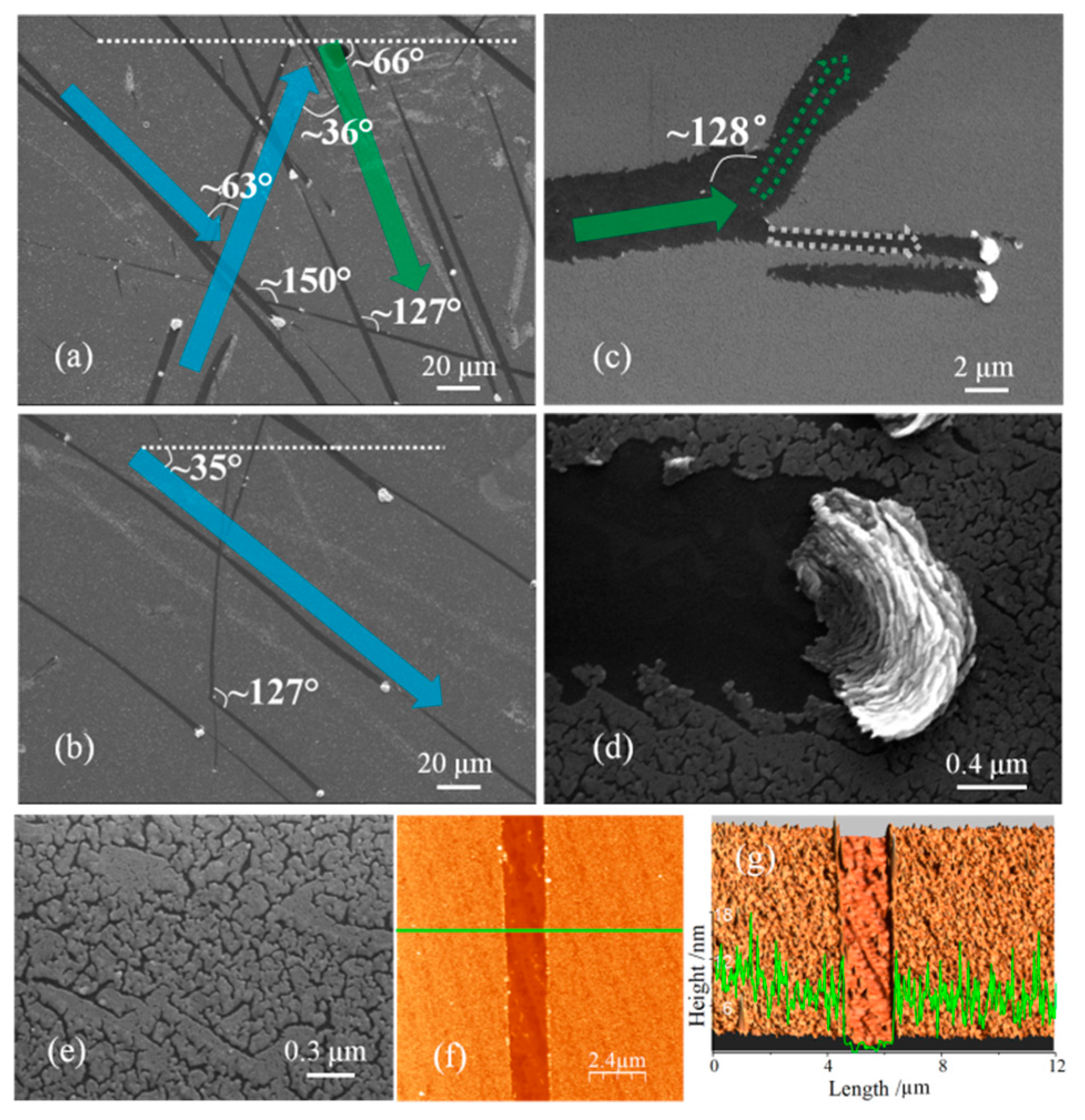
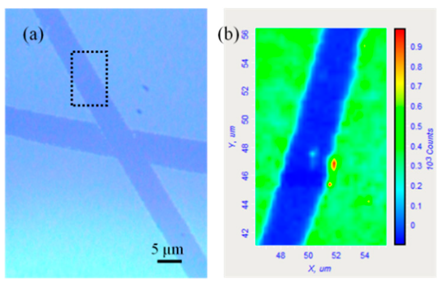
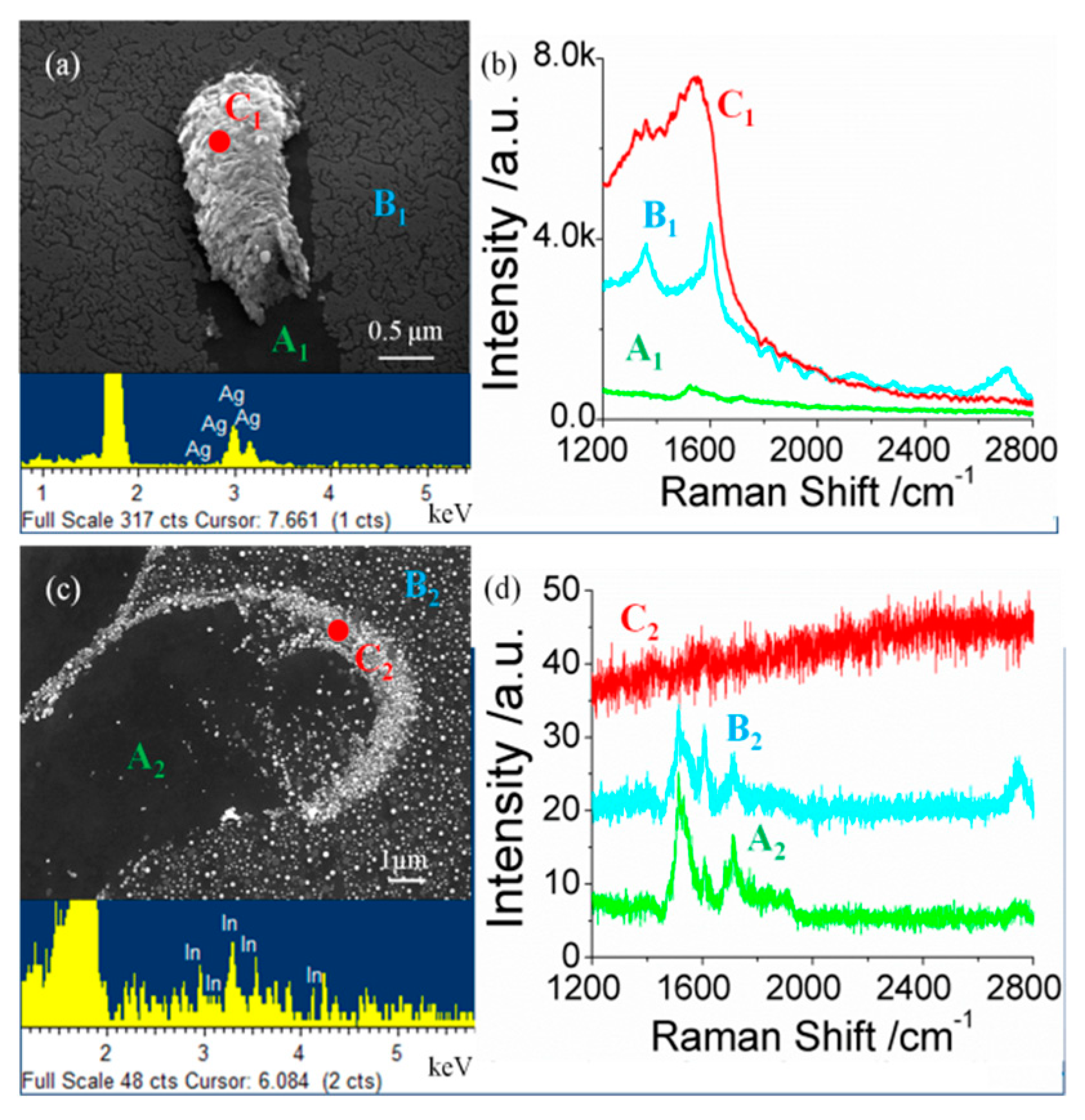
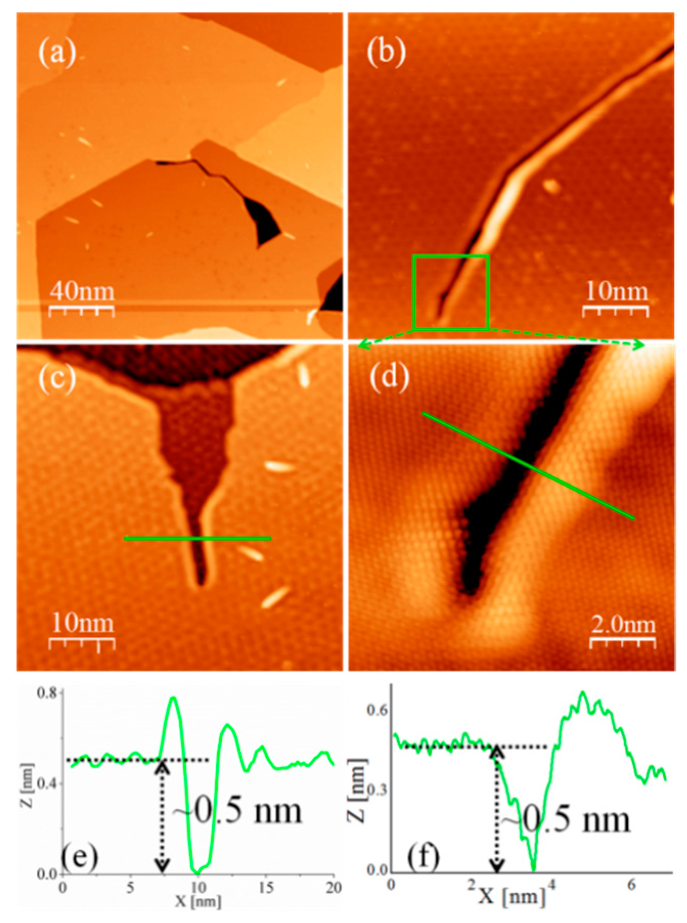
3. Results and Discussions

Figure 1 shows the results of the Ag/EG system observed by SEM and AFM. The formation of trenches is only motivated by sliding of Ag particles during high vacuum annealing. According to the hexagonal structure of the EG substrate, the angle between two armchair/zigzag directions is 60°, and the angle between an armchair and a zigzag is 30° [35]. Similarly, the slipping of metal particles is strictly along some particular directions, which are 30° or 60° with respect to one another. As marked by the green and blue arrows in Figure 1a,b, the slipping directions can be parallel to each other or intersect, and the width is in several microns. As shown in Figure 1a, the white dashed line is marked, from which the green arrow deviates by about ~66°. It indicates the directions of these trenches along the green arrow. The intersected trenches with an angle of ~127° from the green arrow are marked by the green arrow. Some trenches are identified with other directions as marked by the blue arrows, which deviate from the green arrows by ~36° and ~150°. The angle between the two blue arrows in Figure 1a is ~63°. Figure 1b shows another region of the same sample on which the trench directions are parallel to each other. There is an including angle of 35° between the blue arrow and the white dashed line, and the sliding direction can be swerved (~127°) into another one across some defects [36]. Apparently, all these micro-trenches are long and straight. Most of these trenches are parallel and stay in one direction when sliding happens, and the sliding directions might correspond to the some crystallographic orientations of graphene [37].
Figure 1c,d show more details of trenches in an enlarged area by SEM images. Some particles can be swerved or branched into two as indicated by the dashed green and white arrows in Figure 1c. The marked angle of 128° means the diversion of the trenches, and the moving particle can also introduce the parallel sliding of another Ag particle, as shown under the white dashed arrow. Figure 1d displays the head of Ag trench in a magnified area. The large bright particles on the trench is the aggregation of metal particles during sliding, and the wrinkles caused by push and press are clearly evidenced. It rightly demonstrates the sliding direction. That is to say, vacuum annealing can induce the migration of metal particles, because the annealing temperature (~570 K) is much smaller than that of the melting point of Ag (1234 K); it can be deduced that some small Ag particles would be melted partly at such high vacuum annealing [38], and a tiny perturbation would push Ag particles to move forward and form a trench on graphene sheets. Moreover, the small Ag particles would merge into larger ones gradually as a result of a snowballing effect during sliding as shown in Figure 1d. After that, the large particle with wrinkles ahead of the trench can be clearly visible in the SEM images. Figure 1e displays the surface area without trenches, only showing the morphology of Ag thin films on EG after annealing. The sliding of Ag particles breaks the continuity of Ag films. Figure 1f,g show the AFM morphology and corresponding 3D image, from which SiC steps inside the trench is clearly observed. The straight trench is in depth of ~8.0 nm and in width of ~4.0 μm as marked by the green profile. Even across SiC steps, the vacuum annealing is still enough to make the sliding of Ag particles.
Similarly, trenches can be produced by the sliding of In particles, too. Figure 2a,b display the macroscopic morphology of trenches on EG, in which the white dashed lines are also used to denote one direction. Figure 2a shows large numbers of paralleling trenches with an angle of ~7° from the white dashed line, and the distance between each channel is randomly. The trenches with the direction highlighted by the green arrow in Figure 2b deviates from the white dashed line by an angle of ~67°, other trenches have an angle of 116°–118° with the green arrow. Meanwhile, some trenches are formed with an angle of ~35° using the green arrow. Figure 2c shows the enlarged image of the paralleling and straight channels, in which the clean substrate after sliding can be observed. As shown in Figure 2d, the sliding can be also swerved at some defects. Figure 1e displays the surface area without trenches, only showing the morphology of In particles on EG. Because the annealing temperature (~570 K) is higher than the melting point (430 K) of In, which is enough to melt In islands on EG, the migration of In particles is extremely easy, and they will be solidified into ball-shaped morphology after annealing. As a result, the sliding of In particles is much easier and a few randomly orientated trenches will be observed as marked by the dashed cycles in Figure 2b. Moreover, the morphology of the In trench head is greatly different from those of Ag trenches. Many small In particles instead of one large particle are scattered around the trench heads. The bright and small particles shown in Figure 2e are the starting sites for particle sliding for the formation of In trenches. Figure 1f,g show the AFM morphology and corresponding 3D image, from which the trench as well as In partilces are clearly observed. As exhibited by the green height profile, the depth and width of In trench are is ~10 nm and ~2.0 μm. It indicates that vacuum annealing is enough to move the In particles to form macro-trenches.
At first sight, the micro-trenches should be surface scratches. Actually, they are produced through the sliding of metal particles which happens only though high vacuum annealing. In previous reports, nano-particles induced etching of graphene was commonly under catalytic gas. For example, particle cutting happens in H2 gas after annealing, and the etching can be controlled along zigzag or armchair directions [37], but most of the cutting direction is uncontrollable and randomly distributed, especially under O2 gas, owing to the anisotropic interactions [36]. However, the formation of micro-trenches in this research is only through high vacuum annealing without any catalytic gas. It is extremely simple for the sliding of metal particles regardless of graphene pits or SiC steps, and most of the trenches are highly orientated and parallel. As shown by the image of Figure 3a tested through optical microscopy (OM), the trenches are stable even exposed under atmosphere for many days. Figure 3b displays the Raman mapping of 2D-band measured from the dashed black rectangle region in Figure 3a. For the Raman mapping tested inside the trench, the intensity of 2D-band is much weaker than of the flat area. It is indicated that graphene sheets are damaged by the friction and a similar etching effect is achieved.
Figure 4 shows more details about the two types of trenches by enlarged SEM images and corresponding Raman spectra. As shown in Figure 4a, there are three different regions, inside trench, Ag film without sliding and the trench head, which are marked as A1, B1 and C1, respectively. As shown in the lower part of Figure 4a, elemental analysis (EDS) is conducted to prove Ag particles which is measured from the red point marked in Figure 4a. Figure 4b shows the Raman spectra detected from each site, and a big difference can be distinguished. On region (B1) covered by Ag films without any sliding, it exhibits the classical Raman peaks of EG located at ~1350 cm−1, ~1590 cm−1 and ~2700 cm−1. The enhanced intensity around 1200 cm−1 to 1800 cm−1 represents the surface enhanced Raman spectra (SERS) by Ag particles, which is commonly observed [39,40,41]. There are big difference inside trench (A1) and on Ag trench head (C1). Raman peaks of graphene nearly disappears inside trench, only showing fairly weak Raman peaks of SiC substrate. The Raman peak on Ag trench head exhibits a typical structure of diamond-like carbon (DLC), which means amorphous carbon (α-C) is merged into Ag particle [42,43]. The difference of Raman spectra rightly demonstrates that graphene sheets can be damaged during the sliding of Ag particles. Carbon atoms can transform to amorphous carbon and merge into Ag particles. Figure 4c,d display the similar phenomenon on In/EG system. As shown in Figure 4c, inside trench, In particles without sliding and the trench head are also marked by A2, B2 and C2, respectively. As shown in the lower part of Figure 4c, EDS analysis measured from the red point marked in Figure 4c can prove In particles on EG sheets. As shown in Figure 4d, normal Raman feature of EG is observed on the region of In particles without sliding. The Raman spectra of A2 and B2 do not differ strongly between each other. The peaks located at 1550 and 1700 cm−1 in A2 and B2 are related to the SiC substrate. Different from Ag particles, there is no enhanced intensity observed in In/SiC system due to special metals for SERS detection. hence, the graphene peaks are weak, and the 1350 cm−1 peak is very close to the noise threshold, it is not clearly visible in either A2 and B2 spectrum. But, the graphene peaks in A2 spectrum is much weaker than that in B2 one, which also indicates the damage influence of sliding In particles to EG sheets. Therefore, the sliding behavior of metal particles on EG is only motivated by high vacuum annealing resembles the catalystic etching effect, by which EG can be easily patterned.
It is also found that the EG layer tends to be etched by the metal particles in the process of long time annealing in UHV, and nano-trenches are formed. Figure 5a,b displays the macro-morphology of EG, on which all the metals have been evaporated. Meanwhile, there exist a narrow channel originating from the edge of pits. It is deduced that EG has been scratched and broken by the sliding metal particles even during long term annealing (more than 24 h). The etching always happens at the high energy sites of edges and defective points. Figure 5c shows an enlarged image of one etched channel, and Figure 5d shows the atomic structure of the etched channel zoomed in from the green square in Figure 5b. As exhibited by the height profiles in Figure 5e,f acquired from the green lines in Figure 5c,d, the depth of the channel is about 0.5 nm, consistent with the interlayer distance of graphene. Meanwhile, the edge region is higher than the flat EG, indicating the edge structure caused by the broken of EG sheet. As shown in Figure 5d, there exist interference scattering patterns along the channel [44], meaning that a broken of continuity of EG layer and new edge has been formed. The profile heights and the atomically resolved structures prove that only the top EG layer has been etched.
The formation mechanism of nano-trenches on EG layers is complex, but the most possible reason may also be related to oxidation of carbon atoms, and metal particles can be activated to move forward and scissor graphene sheets gradually at elevated temperatures [17,18]. Oxygen may be released from the chamber or the sample surface, and only a very small amount is contained. That is why the etching cannot be commonly observed, and happens only around the edges or defective sites because of high energy dangling bonds. The etching also happens on the terrace and the defective point is considered as the triggered sites. The formation mechanism of nano-trenches is helpful for the patterning of graphene.

4. Conclusions

In summary, an interesting sliding behavior of metal particles (Ag and In) and long straight micro-trenches on EG induced by UHV annealing are investigated. Most of the micro-trenches are highly orientated and parallel to each other. Meanwhile, the EG structure can be scratched and erased easily because of friction during sliding and confirmed by Raman mapping and spectra. Combined with the characterization of atomically resolved STM, a similar etching effect can be evidenced and achieved. The finding will help us to understand more properties about the mutual effect of metals on EG, and might provide us a new and easy way to make structured EG.

Author Contributions

Conceptualization, K.X. and F.M.; Methodology, T.H.; Software, D.M.; Validation, T.H. and F.M.; Formal Analysis, T.H.; Investigation, X.L. and R.W.; Resources, K.X.; Data Curation, F.M.; Writing-Original Draft Preparation, T.H.; Writing-Review & Editing, F.M.; Visualization, F.M.; Supervision, K.X.; Project Administration, K.X.; Funding Acquisition, T.H. and F.M.

Funding

This work was jointly supported by National Natural Science Foundation of China (Grant Nos. 51601142, 51771144, 51471130), China Postdoctoral Science Foundation (2016M592785), Natural Science Foundation of Shaanxi Province (No. 2017JZ015), Fundamental Research Funds for the Central Universities and Collaborative Innovation Center of Suzhou Nano Science and Technology.

Conflicts of Interest

The authors declare no conflicts of interest.

References

  1. Novoselov, K.S.; Fal’ko, V.I.; Colombo, L.; Gellert, P.R.; Schwab, M.G.; Kim, K. A roadmap for graphene. Nature 2012, 490, 192–200. [Google Scholar] [CrossRef]
  2. Zhang, T.; Wu, S.; Yang, R.; Zhang, G. Graphene: Nanostructure engineering and applications. Front. Phys. 2017, 12, 127206. [Google Scholar] [CrossRef]
  3. Yu, R.; Manjavacas, A.; Garcia de Abajo, F.J. Ultrafast radiative heat transfer. Nat. Commun. 2017, 8, 2. [Google Scholar] [CrossRef] [PubMed]
  4. Novoselov, K.S.; Geim, A.K.; Morozov, S.V.; Jiang, D.; Zhang, Y.; Dubonos, S.V.; Grigorieva, I.V.; Firsov, A.A. Electric field effect in atomically thin carbon films. Science 2004, 306, 666–669. [Google Scholar] [CrossRef] [PubMed]
  5. Cai, J.; Ruffieux, P.; Jaafar, R.; Bieri, M.; Braun, T.; Blankenburg, S.; Muoth, M.; Seitsonen, A.P.; Saleh, M.; Feng, X.; et al. Atomically precise bottom-up fabrication of graphene nanoribbons. Nature 2010, 466, 470–473. [Google Scholar] [CrossRef] [PubMed]
  6. Yang, W.; Chen, G.; Shi, Z.; Liu, C.; Zhang, L.; Xie, G.; Cheng, M.; Wang, D.; Yang, R.; Shi, D.; et al. Epitaxial growth of single-domain graphene on hexagonal boron nitride. Nat. Mater. 2013, 12, 792–797. [Google Scholar] [CrossRef]
  7. Zheng, Y.; Wang, H.; Hou, S.; Xia, D. Lithographically defined graphene patterns. Adv. Mater. Technol. 2017, 2, 1600237. [Google Scholar] [CrossRef]
  8. Geng, D.; Wang, H.; Wan, Y.; Xu, Z.; Luo, B.; Xu, J.; Yu, G. Direct top-down fabrication of large-area graphene arrays by an in situ etching method. Adv. Mater. 2015, 27, 4195–4199. [Google Scholar] [CrossRef]
  9. Wang, X.; Dai, H. Etching and narrowing of graphene from the edges. Nat. Chem. 2010, 2, 661–665. [Google Scholar] [CrossRef] [PubMed]
  10. Chen, K.; Chu, T.; Wu, C.; Lee, S.; Lin, S. Atomic layer etchings of transition metal dichalcogenides with post healing procedures: Equivalent selective etching of 2D crystal hetero-structures. 2D Mater. 2017, 4, 034001. [Google Scholar] [CrossRef]
  11. Lukas, M.; Meded, V.; Vijayaraghavan, A.; Song, L.; Ajayan, P.M.; Fink, K.; Wenzel, W.; Krupke, R. Catalytic subsurface etching of nanoscale channels in graphite. Nat. Commun. 2013, 4, 1379. [Google Scholar] [CrossRef] [PubMed] [Green Version]
  12. Oberhuber, F.; Blien, S.; Schupp, F.; Weiss, D.; Eroms, J. Anisotropic etching of graphene in inert and oxygen atmospheres. Phys. Status Solidi A 2017, 214, 1600459. [Google Scholar] [CrossRef]
  13. Schröder, U.A.; Grånäs, E.; Gerber, T.; Arman, M.A.; Martínez-Galera, A.J.; Schulte, K.; Andersen, J.N.; Knudsen, J.; Michely, T. Etching of graphene on Ir(111) with molecular oxygen. Carbon 2016, 96, 320–331. [Google Scholar] [CrossRef]
  14. Leong, W.S.; Gong, H.; Thong, J.T.L. Low-contact-resistance graphene devices with nickel-etched-graphene contacts. ACS Nano 2014, 8, 994–1001. [Google Scholar] [CrossRef]
  15. Ma, L.; Wang, J.; Yip, J.; Ding, F. Mechanism of transition-metal nanoparticle catalytic graphene cutting. J. Phys. Chem. Lett. 2014, 5, 1192–1197. [Google Scholar] [CrossRef]
  16. Qiu, Z.; Song, L.; Zhao, J.; Li, Z.; Yang, J. The nanoparticle size effect in graphene cutting A “Pac-Man” mechanism. Angew. Chem.-Int. Ed. 2016, 55, 9918–9921. [Google Scholar] [CrossRef] [PubMed]
  17. Jin, J.E.; Lee, J.-H.; Choi, J.H.; Jang, H.-K.; Na, J.; Whang, D.; Kim, D.-H.; Kim, G.T. Catalytic etching of monolayer graphene at low temperature via carbon oxidation. Phys. Chem. Chem. Phys. 2016, 18, 101–109. [Google Scholar] [CrossRef]
  18. Cheng, G.; Calizo, I.; Hacker, C.A.; Richter, C.A.; Hight Walker, A.R. Fe-catalyzed etching of exfoliated graphite through carbon hydrogenation. Carbon 2016, 96, 311–315. [Google Scholar] [CrossRef] [Green Version]
  19. Manadé, M.; Viñes, F.; Illas, F. Transition metal adatoms on graphene: A systematic density functional study. Carbon 2015, 95, 525–534. [Google Scholar] [CrossRef]
  20. Liu, X.; Wang, C.-Z.; Hupalo, M.; Lin, H.-Q.; Ho, K.-M.; Tringides, M. Metals on graphene: Interactions, growth morphology, and thermal stability. Crystals 2013, 3, 79–111. [Google Scholar] [CrossRef]
  21. Legesse, M.; Mellouhi, F.E.; Bentria, E.T.; Madjet, M.E.; Fisher, T.S.; Kais, S.; Alharbi, F.H. Reduced work function of graphene by metal adatoms. Appl. Surf. Sci. 2017, 394, 98–107. [Google Scholar] [CrossRef] [Green Version]
  22. Liu, X.T.; Hu, T.W.; Miao, Y.P.; Ma, D.Y.; Chu, P.K.; Ma, F.; Xu, K.W. Selective growth of Pb islands on graphene/SiC buffer layers. J. Appl. Phys. 2015, 117, 065304. [Google Scholar] [CrossRef]
  23. Hu, T.; Hui, X.; Zhang, X.; Liu, X.; Ma, D.; Wei, R.; Xu, K.; Ma, F. Nanostructured Bi Grown on Epitaxial Graphene/SiC. J. Phys. Chem. Lett. 2018, 9, 5679–5684. [Google Scholar] [CrossRef] [PubMed]
  24. Oh, J.; Kim, K.; Yeom, G. Graphene doping methods and device applications. J. Nanosci. Nanotechnol. 2014, 14, 1120–1133. [Google Scholar] [CrossRef] [PubMed]
  25. Kim, S.; Shin, S.; Kim, T.; Du, H.; Song, M.; Kim, K.; Lee, S.; Seo, S. A reliable and controllable graphene doping method compatible with current CMOS technology and the demonstration of its device applications. Nanotechnology 2017, 28, 175710. [Google Scholar] [CrossRef] [PubMed]
  26. Dianat, A.; Liao, Z.; Gall, M.; Zhang, T.; Gutierrez, R.; Zschech, E.; Cuniberti, G. Doping of graphene induced by boron/silicon substrate. Nanotechnology 2017, 28, 215701. [Google Scholar] [CrossRef]
  27. Hu, T.; Fang, Q.; Zhang, X.; Liu, X.; Ma, D.; Wei, R.; Xu, K.; Ma, F. Enhanced n-doping of epitaxial graphene on SiC by bismuth. Appl. Phys. Lett. 2018, 113, 011602. [Google Scholar] [CrossRef]
  28. Hardcastle, T.P.; Seabourne, C.R.; Zan, R.; Brydson, R.M.D.; Bangert, U.; Ramasse, Q.M.; Novoselov, K.S.; Scott, A.J. Mobile metal adatoms on single layer, bilayer, and trilayer graphene: An ab initio DFT study with van der Waals corrections correlated with electron microscopy data. Phys. Rev. B 2013, 87, 195430. [Google Scholar] [CrossRef]
  29. Asadi, K.; Timmering, E.C.; Geuns, T.C.; Pesquera, A.; Centeno, A.; Zurutuza, A.; Klootwijk, J.H.; Blom, P.W.; de Leeuw, D.M. Up-scaling graphene electronics by reproducible metal-graphene contacts. ACS Appl. Mater. Interfaces 2015, 7, 9429–9435. [Google Scholar] [CrossRef]
  30. Anithaa, V.S.; Shankar, R.; Vijayakumar, S. Adsorption of Mn atom on pristine and defected graphene: A density functional theory study. J. Mol. Model. 2017, 23, 132. [Google Scholar] [CrossRef]
  31. García-Rodríguez, D.E.; Mendoza-Huizar, L.H.; Díaz, C. A DFT study of Cu nanoparticles adsorbed on defective graphene. Appl. Surf. Sci. 2017, 412, 146–151. [Google Scholar] [CrossRef]
  32. Pallecchi, E.; Lafont, F.; Cavaliere, V.; Schopfer, F.; Mailly, D.; Poirier, W.; Ouerghi, A. High electron mobility in epitaxial graphene on 4H-SiC(0001) via post-growth annealing under hydrogen. Sci. Rep. 2014, 4, 4558. [Google Scholar] [CrossRef]
  33. Baringhaus, J.; Ruan, M.; Edler, F.; Tejeda, A.; Sicot, M.; Taleb-Ibrahimi, A.; Li, A.P.; Jiang, Z.; Conrad, E.H.; Berger, C.; et al. Exceptional ballistic transport in epitaxial graphene nanoribbons. Nature 2014, 506, 349–354. [Google Scholar] [CrossRef] [PubMed] [Green Version]
  34. Hu, T.W.; Liu, X.T.; Ma, F.; Ma, D.Y.; Xu, K.W.; Chu, P.K. High-quality, single-layered epitaxial graphene fabricated on 6H-SiC (0001) by flash annealing in Pb atmosphere and mechanism. Nanotechnology 2015, 26, 105708. [Google Scholar] [CrossRef] [PubMed]
  35. Hass, J.; de Heer, W.A.; Conrad, E.H. The growth and morphology of epitaxial multilayer graphene. J. Phys.-Condes. Matter 2008, 20, 323202. [Google Scholar] [CrossRef]
  36. Severin, N.; Kirstein, S.; Sokolov, I.M.; Rabe, J.P. Rapid trench channeling of graphenes with catalytic silver nanoparticles. Nano Lett. 2009, 9, 457–461. [Google Scholar] [CrossRef] [PubMed]
  37. Ci, L.; Xu, Z.; Wang, L.; Gao, W.; Ding, F.; Kelly, K.F.; Yakobson, B.I.; Ajayan, P.M. Controlled nanocutting of graphene. Nano Res. 2008, 1, 116–122. [Google Scholar] [CrossRef]
  38. Courty, A.; Henry, A.I.; Goubet, N.; Pileni, M.P. Large triangular single crystals formed by mild annealing of self-organized silver nanocrystals. Nat. Mater. 2007, 6, 900–907. [Google Scholar] [CrossRef]
  39. Zhao, H.; Guo, Y.; Zhu, S.; Song, Y.; Jin, J.; Ji, W.; Song, W.; Zhao, B.; Yang, B.; Ozaki, Y. Facile synthesis of silver nanoparticles/carbon dots for a charge transfer study and peroxidase-like catalytic monitoring by surface-enhanced Raman scattering. Appl. Surf. Sci. 2017, 410, 42–50. [Google Scholar] [CrossRef]
  40. Sun, Q.; Zhang, Y.; Sun, L.; Yang, Y.; Min, C.; Zhu, S.; Yuan, X. Microscopic surface plasmon enhanced raman spectral imaging. Opt. Commun. 2017, 392, 64–67. [Google Scholar] [CrossRef]
  41. Xu, W.; Mao, N.; Zhang, J. Graphene: A platform for surface-enhanced Raman spectroscopy. Small 2013, 9, 1206–1224. [Google Scholar] [CrossRef] [PubMed]
  42. Hatakeyama, T.; Kometani, R.; Warisawa, S.i.; Ishihara, S. Selective graphene growth from DLC thin film patterned by focused-ion-beam chemical vapor deposition. J. Vac. Sci. Technol. B 2011, 29, 06FG04. [Google Scholar] [CrossRef]
  43. Chu, P.K.; Li, L. Characterization of amorphous and nanocrystalline carbon films. Mater. Chem. Phys. 2006, 96, 253–277. [Google Scholar] [CrossRef]
  44. Tesch, J.; Leicht, P.; Blumenschein, F.; Gragnaniello, L.; Bergvall, A.; Löfwander, T.; Fonin, M. Impurity scattering and size quantization effects in a single graphene nanoflake. Phys. Rev. B 2017, 95, 075429. [Google Scholar] [CrossRef]
Figure 1. (a,b) macro view of Ag trenches after UHV annealing. (c) swerved and branched particle due to the defective point. (d) the details of Ag trench heads. (e) surface morphology of Ag thin film on EG without sliding trenches. (f) AFM image of trench after the sliding of Ag particles. (g) corresponding 3D image. The scale bars are marked in each image.
Applsci 08 02518 g001
Figure 2. (a,b) Macro view of In trenches. (ce) Magnified image showing more details about In trenches. (f) AFM image of one trench after the sliding of In particles. (g) Corresponding 3D image. The scale bars are marked in each image.
Applsci 08 02518 g002
Figure 3. (a) The morphology of EG under optical microscopy. (b) Raman mapping of 2D-band measured from the dashed black rectangle region in (a).
Applsci 08 02518 g003
Figure 4. SEM image and corresponding Raman spectroscopy. (a,b) For Ag/EG system, inside trench, Ag film without sliding and the trench head are marked by A1, B1 and C1, respectively. (c,d) for In/EG system, inside trench, In particles without sliding and the trench head are marked by A2, B2 and C2, respectively. EDS results are displayed in the insets.
Applsci 08 02518 g004
Figure 5. (a,b) The macro-morphology of EG with etched channels. (c) An enlarged image about one etched channel. (d) The atomic structure of the etched channel. (e,f) The height profiles acquired from the green lines in (c,d).
Applsci 08 02518 g005

