Article

Experimental Analyses on Multiscale Structural and Mechanical Properties of ε-Si/GeSi/C-Si Materials

1
Tianjin Key Laboratory of Modern Engineering Mechanics, Department of Mechanics, Tianjin University, Tianjin 300072, China
2
Department of Electrical and Computer Engineering, University of Nebraska-Lincoln, Lincoln, NE 68588-0511, USA
3
Institute of Applied Mechanics, Zhejiang University, Hangzhou 310027, China
4
Institute of Microelectronics, Tsinghua University, Beijing 100084, China
*
Authors to whom correspondence should be addressed.
Appl. Sci. 2018, 8(12), 2333; https://doi.org/10.3390/app8122333
Submission received: 30 October 2018 / Revised: 19 November 2018 / Accepted: 19 November 2018 / Published: 22 November 2018
(This article belongs to the Special Issue Precision Dimensional Measurements)

Abstract

:
Strained silicon (ε-Si) is a promising material that could extend Moore’s law by enhancing electron mobility. A ε-Si material is usually composed of multiscale, multilayer heterostructures, where the strained-silicon film or strap is tens-of-nanometers thick, and its buffer layers are of the micrometer scale. The structural properties determine the electrical performance and reliability of ε-Si-based devices. Inhomogeneous residual stress is induced during the preparation, which induces ε-Si structure failure. In this work, biaxial strained-silicon films that contain graded and relaxed germanium-silicon buffer layers were prepared on monocrystalline silicon wafers through reduced-pressure chemical-vapor epitaxy. The layer components and thicknesses were measured using energy-dispersive spectroscopy and scanning-electron microscopy. Crystal and lattice characters were observed by using high-resolution transmission-electron microscopy and micro-Raman spectroscopy. The residual stress distribution along cross-sections of the ε-Si multilayer structures was examined by using micro-Raman mapping. The experimental results showed that, with a gradual increase in germanium concentration, the increasing residual stress was suppressed owing to dislocation networks and dislocation loops inside the buffer layers, which favored the practical application.

1. Introduction

Strained silicon (ε-Si) is regarded as a promising material that could extend Moore’s law [1]. Because introduced strain leads to an increased carrier mobility and reduced resistance [2], the performance of ε-Si-based devices is improved significantly [3]. In recent years, with continuous developments in ε-Si technology, semiconductor chips have become smaller, faster, and more energy efficient [4]. Strained-silicon technology has been applied widely in core chips inside mobile phones, personal computers, laptops, tablets and even televisions [5].
The ε-Si structure complexity determines the difficulty of the manufacturing process. In general, ε-Si is achieved by manufacturing a set of multiscale, multilayer heterogeneous two- or three-dimensional structures [6]. The manufacture of such a complex structure requires a strict and well-designed control of process parameters to ensure that each processing procedure step may yield a material/structure that meets the design requirements of geometrical dimensions and structural-mechanical properties [7,8]. Furthermore, the design, manufacture, performance evaluation and control technologies for microelectronics with non-uniform and local-singular stress distribution is regarded as the future of the microelectronics industry [9].
The (equal biaxial or uniaxial) strain state and its magnitude determine the optical/electrical properties of ε-Si-based devices [10]. The strain state and magnitude of the ε-Si depend heavily on the buffer-layer properties (such as the element composition, thickness, lattice quality, defects and residual stress) and interfacial properties (such as mismatch and shear stress) [11]. Size miniaturization of a ε-Si-based device leads to increased defect densities and residual stress, which results in a degraded optoelectronic performance and structure reliability of the entire integrated device [12].
Experimental studies of multilayer heterogeneous structures, such as strained-silicon, face two major challenges, namely, “multiscale” and “multiproperty coupling”. A strained-silicon layer is usually several to tens-of-nanometers thick, whereas the buffer-layer thickness tends to be of the micrometer scale, and the substrate is typically several hundreds of microns thick. Unique key physical and mechanical behaviors that interact exist at each spatial scale. Cross-scale interactions between the multiscale physical–mechanical properties increase the complexity of experimental studies of strain silicon.
A number of methods at different spatial scales have been applied to experimental studies on multilayer heterogeneous structures [13,14,15,16]. The profiler has been used to measure the average residual stress from the mesoscale [17]. By using (scanning- and transmission-) electron microscopy, the structural morphology and dislocation distribution in the microscale have been determined [18]. At the same scale, nano-indentation has been used to measure the modulus [19], whereas Raman microscopy has been applied to characterize the lattice quality and residual stress [20,21,22]. High-resolution transmission-electron microscopy (TEM) has been used to analyze the lattice structure and local strain of materials at the nanoscale [23].
However, most widely used experimental methods can measure or characterize only one or several material parameters at their respectively applicable scales. These techniques do not provide sufficient understanding of the multiscale structure properties, such as strained silicon, and it is difficult to discover the interaction between the different structural and mechanical properties at different spatial scales. Therefore, there is a need for collaborative analysis using methods at different spatial scales to investigate the interaction mechanisms of multiproperty coupling.
In this work, a biaxial strained-silicon material with germanium–silicon as a buffer layer was prepared and studied experimentally. The structural properties, including the components and thickness of each layer at the microscale and the crystal and lattice characteristics and quality at the nanoscale, was characterized by energy-dispersive spectroscopy (EDS), scanning-electron microscopy (SEM), micro-Raman spectroscopy (MRS) and TEM. The residual stress distribution at different depths was analyzed by using micro-Raman mapping on the sample cross-section.

2. Materials and Methods

The ε-Si/GeSi/C-Si materials were prepared through reduced pressure chemical vapor epitaxy (CVE) [24]. SiH2Cl2 was used as the Si precursor, GeCl4 was the Ge precursor, and H2 was the carrier gas. The monocrystalline Si (100) wafer was pre-treated using an H2SO4:H2O2 = 3:1 solution for 10 min to remove contaminants and then dipped in 10% HF solution to remove the oxide layer. The CVE growth temperature was 900 °C, and the pressure was 1.33 × 10⁴ Pa. In the beginning, the Ge component increased linearly to form a graded germanium-silicon (GexSi1−x, x = 0→0.2) buffer layer of ~3 μm thickness. The growth rate slowed and the Ge concentration was fixed at 20% to form a Ge0.2Si0.8 buffer layer of ~0.8 μm thickness. A 10 nm strained-silicon cap layer was deposited at 750 °C and 1.33 × 10⁴ Pa. Figure 1a provides a schematic structure of the prepared ε-Si/GeSi/C-Si material.
The cross-sectional samples were prepared as follows. A Si-based ε-Si/GeSi wafer was cut to approximately 10 mm × 10 mm square pieces. Two wafers were pasted by using epoxy resin with the ε-Si films face-to-face. Then, two C-Si pieces, cut from another (100) silicon wafer with a 430 μm thickness were pasted outside the two ε-Si/GeSi wafers, respectively. Then, this piece group was cut to some thin slices about a ~1 mm thickness. The two cross-section surfaces of each thin slice were polished by using the chemical-mechanical polishing technique (CMP). Samples for TEM analysis were thinned further by using sandpaper (3M, Maplewood, Minnesota, USA), lapping film (Allied High Tech Products, Rancho Dominguez, CA) and a precise ion-polishing machine (Gatan, Pleasanton, CA, USA).
A ZEISS EVO MA15 system and a JEOL 2100 system were used for the SEM and TEM tests, respectively. Raman experiments for the cross-sectional samples were conducted by using a laser confocal micro-Raman system (InVia Reflex, Renishaw, Gloucestershire, UK) with a 532 nm laser exciting light. A 50× Leica objective (N.A. 0.8) was used, and hence, the spot size of the incident laser was about 1 μm in diameter. Besides, Raman tests on the untreated surface of the strained-silicon samples used the same system, but with a 325-nm laser and a 40× Leica ultraviolet (UV) objective (N.A. 0.5). The sampling spot of the incident laser was about 5 μm in diameter.

3. Results and Discussion

3.1. Microscale Structural Properties

Figure 1b shows an SEM image of the multilayer vicinity of the cross-sectional sample. Because of differences in the electrical resistance of each layer, distinctive monocrystalline silicon, GexSi1−x, Ge0.2Si0.8 and epoxy resin layers were observed. A narrow black strip of ~1 μm thickness is the adhesive layer of epoxy resin that adheres the two multilayer wafers. The region with uniform and relatively deeper greyscale, at the left of the image and far from the adhesive layer, is the C-Si substrate. From the C-Si substrate to the wafer edge (~3.6 μm thickness), the grayscale becomes brighter gradually, which is the graded and relaxed buffer layers. The C-Si/GexSi1−x interface is clear and straight, but that of the GexSi1−x/Ge0.2Si0.8 interface is barely distinguishable visible in this SEM image. The strained-silicon layer (~10 nm thick) is not recognized in the SEM image, because of the resolution limitation of the SEM system.
The SEM image also shows that there is no visible fluctuation on the surface of the sample cross-section. The cross-sectional surface roughness was measured by using an atomic-force microscope (AFM, Dimension Icon, Bruker, Billerica, Massachusetts, USA) and a white-light interferometer (WLI, NewView 8300, Zygo, Middlefield, Connecticut, USA). 
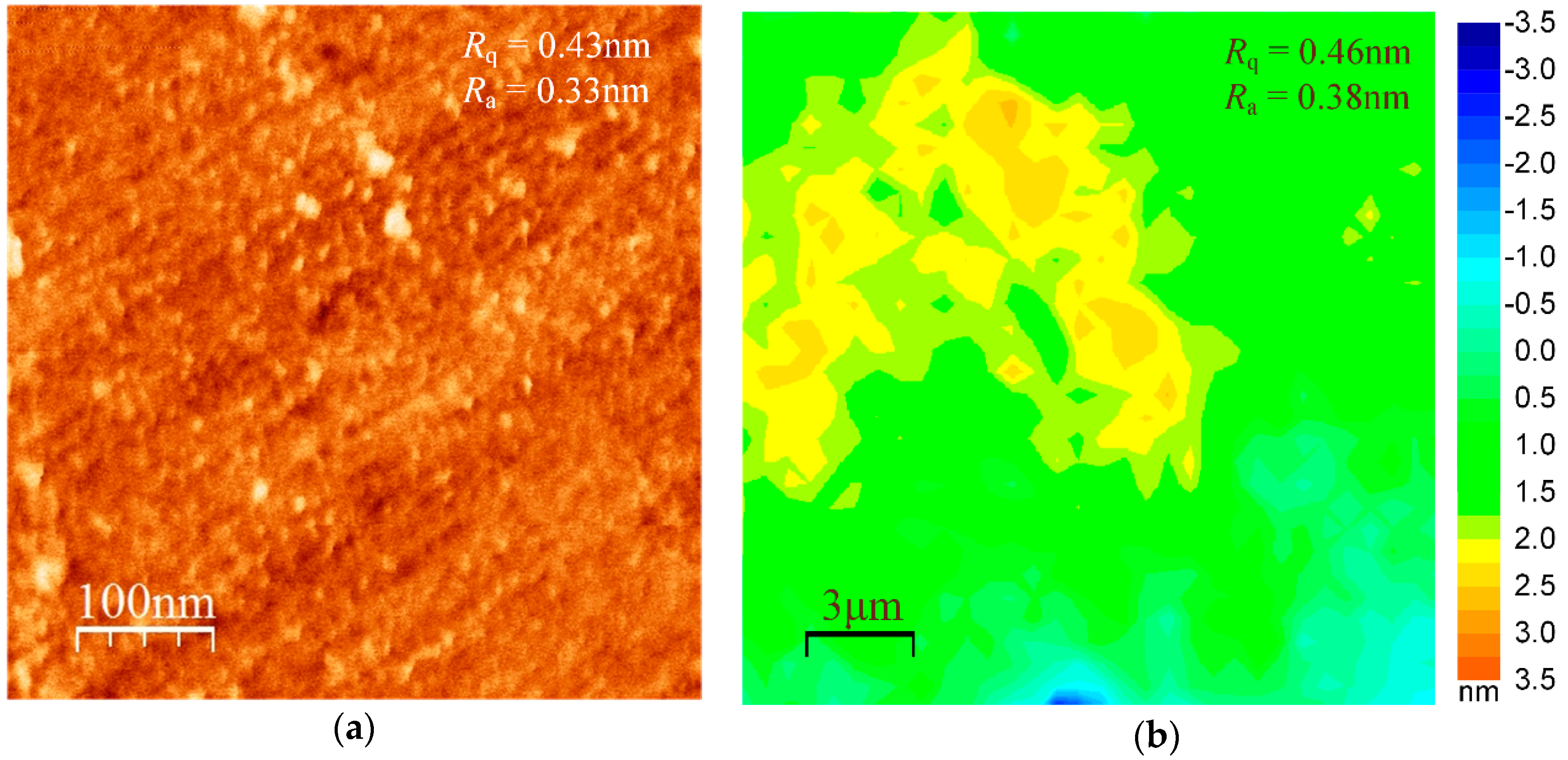
Figure 2a gives the height data of a random 500 nm × 500 nm area on the cross-sectional surface detected by AFM. The root-mean-square deviation of the height data (Rq) is 0.43 nm, and the arithmetical mean deviation of the height data (Ra) is 0.33 nm. Figure 2b gives the height data of a random 21 μm × 21 μm area on the cross-sectional surface detected by using a white-light interferometer with a spatial resolution of 0.34 μm in the X/Y direction and 0.01 nm in the Z direction (root-mean-square repeatability). Rq and Ra are essential surface-roughness parameters. The experimental results showed that the surface roughness of the sample cross-section was less than 0.5 nm, regardless of the nano- or microscale area.
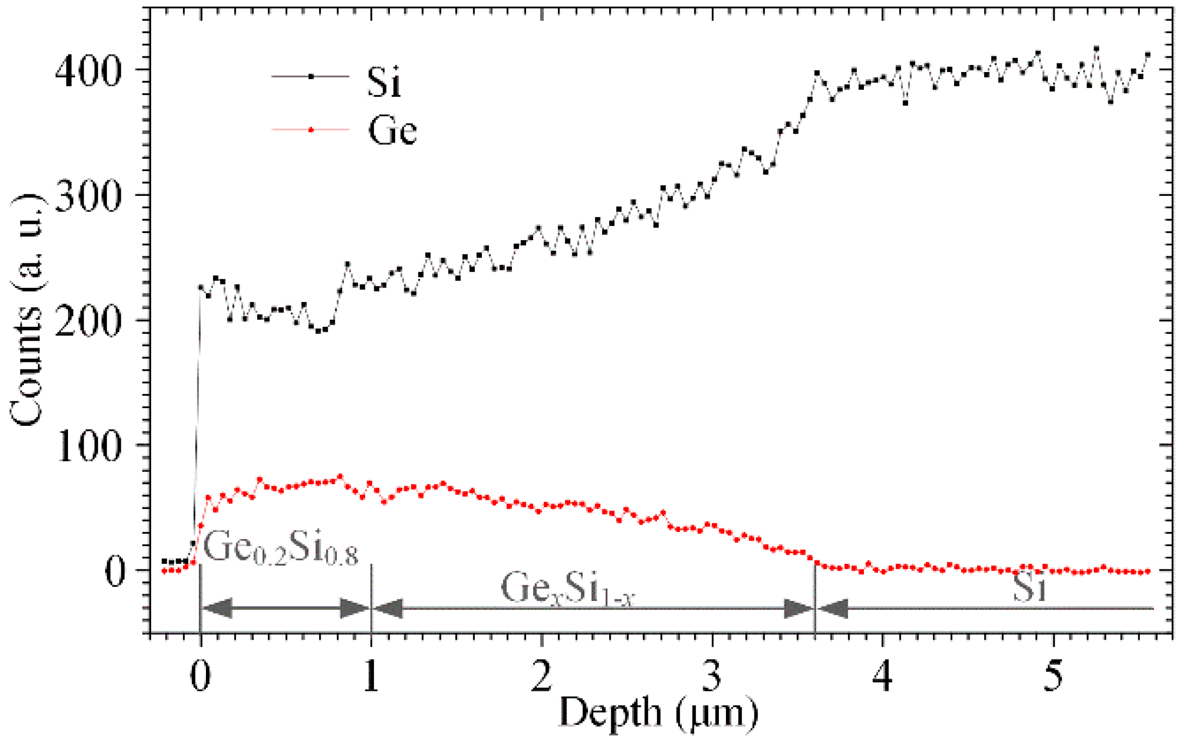
The elemental distribution along the depth direction of the sample cross-section is shown in Figure 3 as determined by EDS (Oxford Instruments, Oxford, UK) with a 42-nm step length. When the EDS sampling point on the cross-section surface approaches the wafer edge, the elemental silicon content exhibits an approximately linear decrease and that of elemental germanium shows a linear increase. Such linear variations of the elemental components that are sustained inside a region of ~2.6 μm in thickness, corresponding to the graded buffer layer (via the GexSi1−x layer).
The content of elemental silicon increased slightly and gradually until the sampling point reached the wafer edge. The opposite behavior resulted in the content of elemental germanium. The thickness of this region was ~1 μm, which corresponds to the relaxed buffer layer (viz. the Ge0.2Si0.8 layer). In this layer, the actual distributions of elemental Si and Ge did not agree with, but were not distinct from, the design shown in Figure 1. The EDS result showed that it was difficult to recognize the interface between the two buffer layers, and the exact thickness of the two buffer layers. The sudden drop of the Si component at a 1 μm depth may have been caused by parameter alternation during the ultra-high-vacuum chemical-vapor epitaxy, which helps to locate the GexSi1−x/Ge0.2Si0.8 interface.
Both elements decreased to zero because the EDS sampling point entered the epoxy resin layer of the sample cross-section. The EDS data did not show the signal from the ε-Si layer, which should be because the ε-Si layer thickness (~10 nm) was less than the EDS sampling step length.
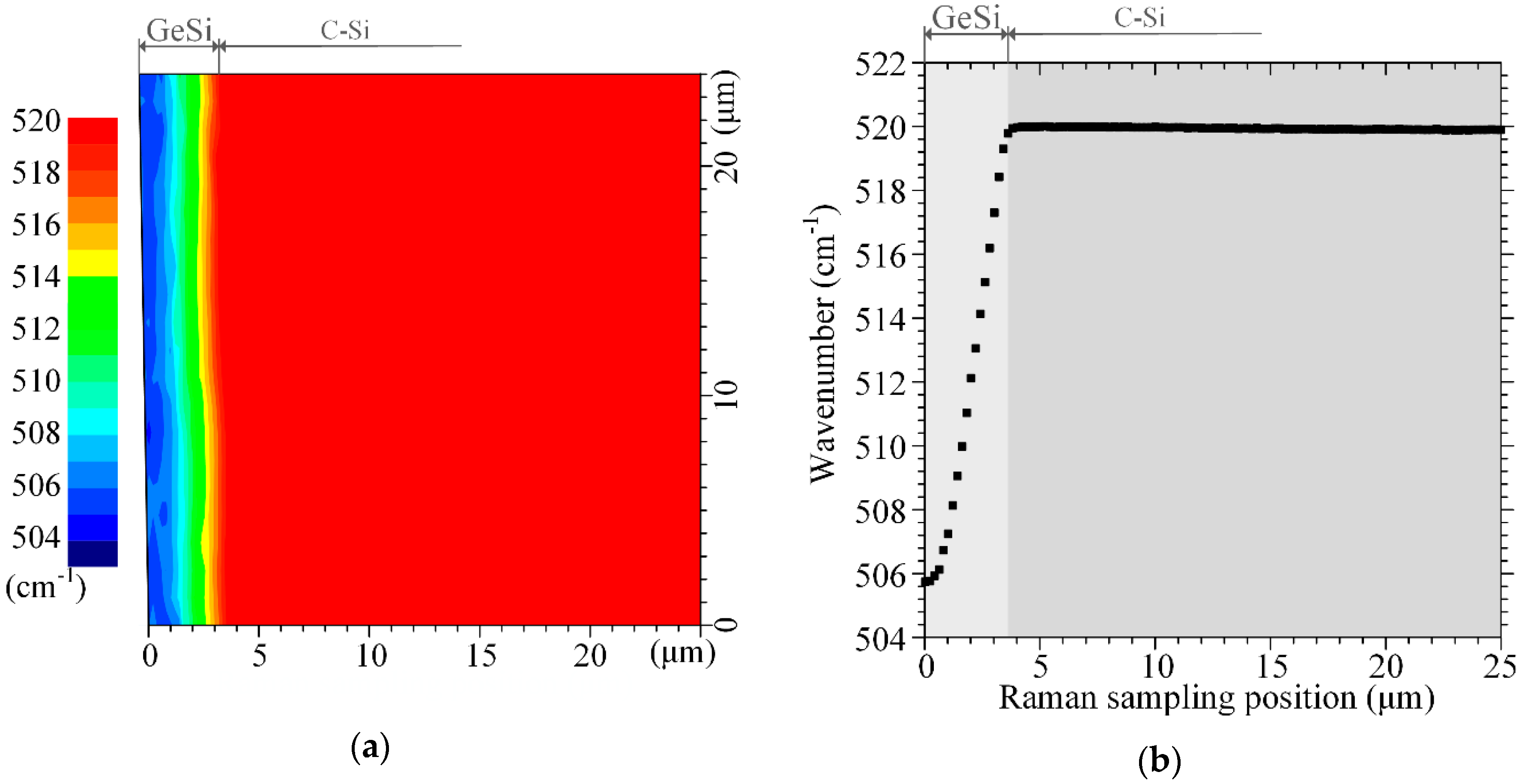
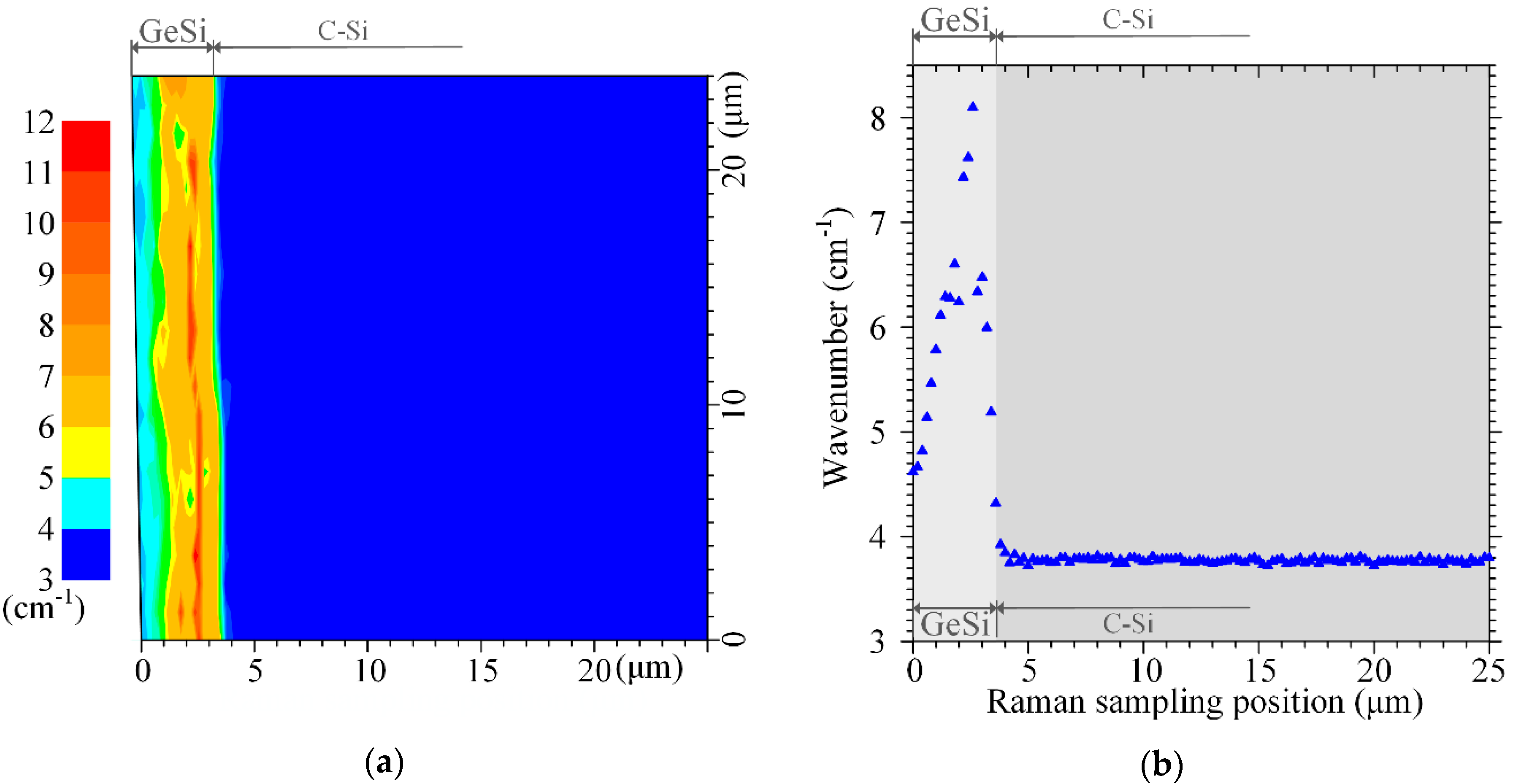
Figure 4a shows the wavenumber image of the Si-Si band (~520 cm−1) that was obtained by Raman mapping at a 25 μm × 24 μm region near the multilayer interfaces on the sample cross-section. The step lengths for Raman mapping along the parallel and vertical direction to the interfaces were 1.2 μm and 0.2 μm, respectively. Figure 4b shows the mean values of the wavenumbers at different locations along the depth direction based on Figure 4a. Figure 4a,b shows that the wavenumber at ~520 cm−1 changes slightly inside the Si substrate, acutely in the buffer layers, and continuously at the interfaces. When the scanning spot originated from the Si substrate into the buffer layers, the wavenumber showed a sharp and linear decrease with a speed of −4.97 ± 0.07 cm−1/μm. However, this rapidly decreasing trend stopped within a region of ~1 μm next to the epoxy layer (compared with the top surface of the strained-silicon wafer), where the wavenumber decreased gently with a speed of −0.83 ± 0.28 cm−1/μm. Hence, from the wavenumber image, the thickness of the rapidly decreased wavenumber region is ~2.6–2.8 μm, and that of the gently decreased wavenumber region is ~0.8–1 μm. The former region is the GexSi1−x layer and the latter is the Ge0.2Si0.8 layer. The strain distribution can be achieved by using the wavenumber results, as discussed below.
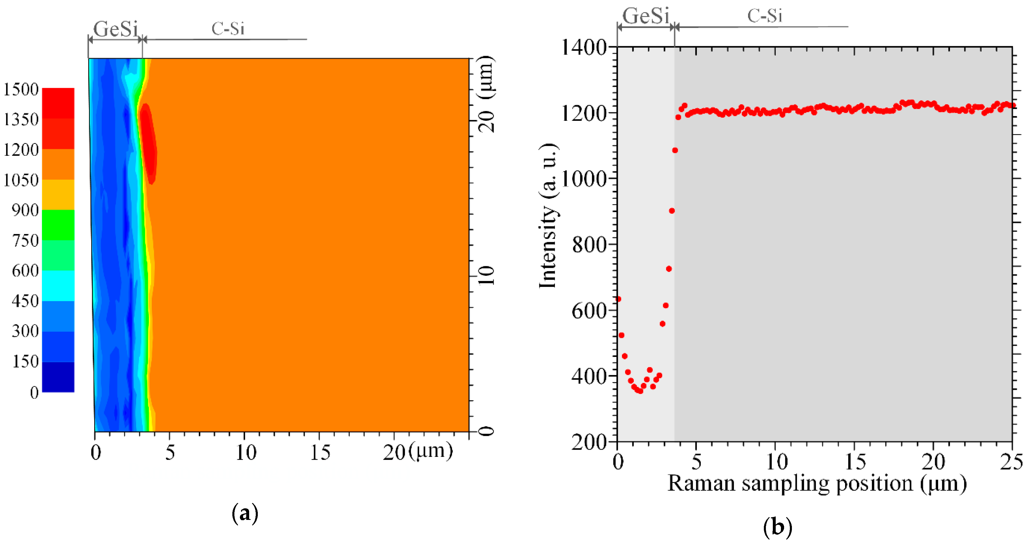
Figure 5a shows the Raman intensity image of the same region in Figure 4a. Figure 5b shows the mean values at different locations along the depth direction based on Figure 5a. In Figure 5, when the sampling spot for Raman mapping from the Si substrate crossed the buffer layer, the Raman intensity of the Si-Si band decreased first and then increased. The Raman-intensity-decreased region in Figure 5 is almost the same as that of the wavenumber rapid-decreased region in Figure 4, so the Raman intensity-increased region to the wavenumber gently-decreased region. This result indicates that the quantity of elemental Si in the monocrystalline stage decreased with a continuous enhancement of elemental Ge in the graded-buffer (GexSi1−x) layer, and then improved gradually inside the relaxed-buffer (Ge0.2Si0.8) layer even though the elemental content of the materials did not change any more.
Figure 6a shows the full-width-at-half-maximum (FWHM) image of the same region of Figure 4a. Figure 6b gives the mean values at different locations along the depth direction based on Figure 6a. In Figure 6, the FWHM of the Si-Si band broadened first and then narrowed when the sampling spot of Raman mapping from the Si substrate crossed the buffer layer. The FWHM broadened region in Figure 6 is different from (smaller than) the wavenumber rapid-decreased region in Figure 4 and the Raman-intensity-decreased region in Figure 5. Therefore, with a continuous enhancement of elemental Ge, the average lattice quality of the Si element in the monocrystalline stage in the graded-buffer (GexSi1−x) layer decreased to an extreme and then improved continuously. This tendency was retained in the relaxed-buffer (Ge0.2Si0.8) layer.

3.2. Nanoscale Structural Properties

The structural properties at the nanoscale were investigated by using TEM. Figure 7 and Figure 8 give high- and low-resolution TEM images of the sample cross-section, respectively. 
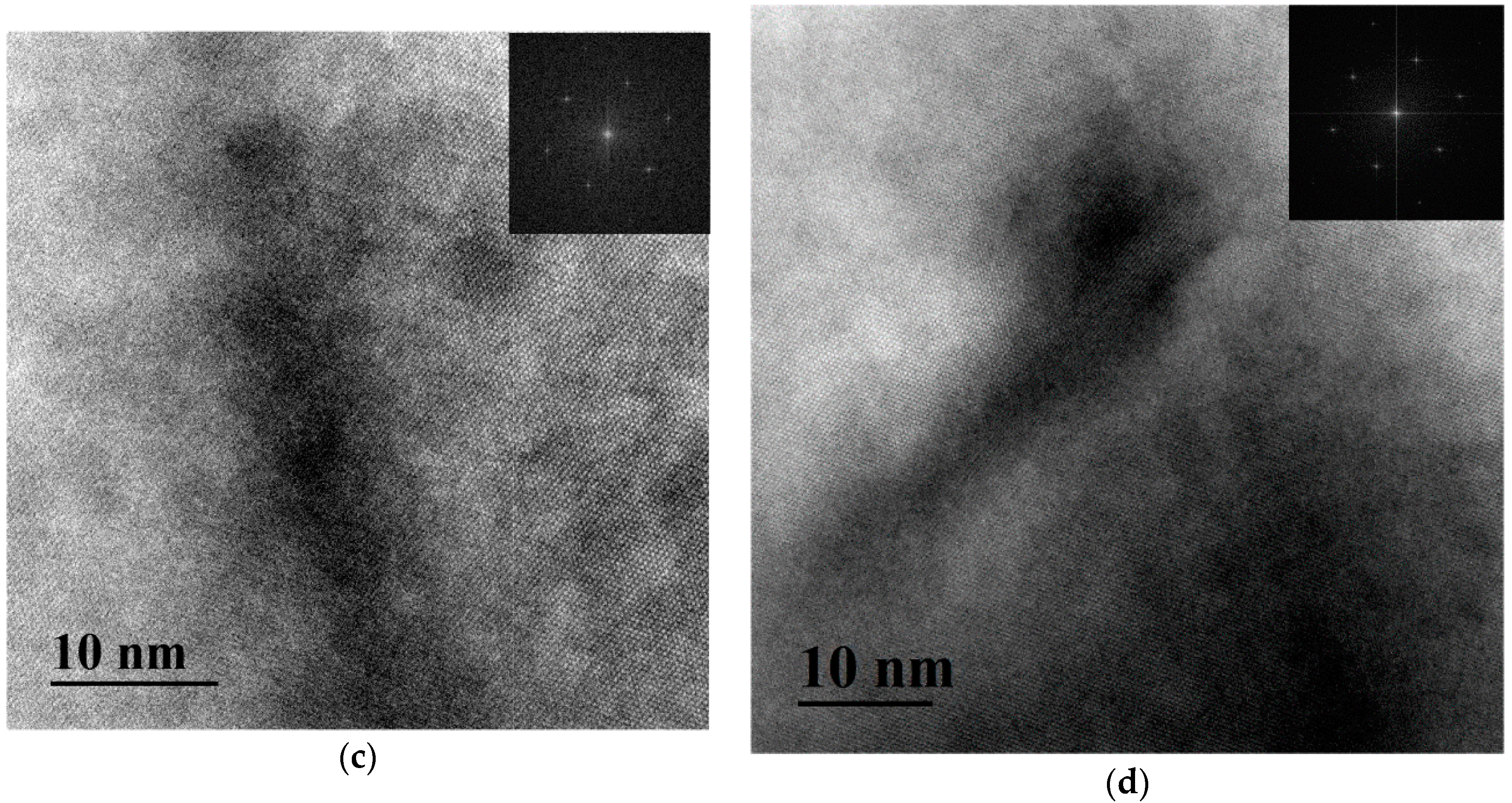
Figure 7a shows a high-resolution TEM image, including the ε-Si and Ge0.2Si0.8 layers. Three regions exist, each of which has a uniform contrast grade, and which corresponds to a dissimilar layer. The left lower region, which is brightest, is an epoxy resin layer of the sample that serves as the adhesive for the two wafers. The image shows no regular lattice structure in this region. The region adjacent to the epoxy is the ε-Si layer. The largest region in the image is the Ge0.2Si0.8 layer. Inside the ε-Si layer, the lattice structure is complete and clear, and shows a regular mesh of the monocrystalline state. The growth surface is in the same atomic sheet. No visible defects exist in this layer. Moreover, the interface of the ε-Si/Ge0.2Si0.8 layers appears clear, straight and almost atomically flat, where the lattices match well. The ε-Si layer thickness is relatively uniform at ~8.67 nm. Figure 7 also shows that the cross-section is a (100) crystal plane.
Figure 8a shows a low-resolution TEM image around the Ge0.2Si0.8 layer, and Figure 7b shows a high-resolution enlarged image of spot A in Figure 8a, which is inside the Ge0.2Si0.8 layer. In the low-resolution TEM image, no obvious defect exists inside the Ge0.2Si0.8 layer. The interface between the GexSi1−x and Ge0.2Si0.8 layers is clearly recognizable, which shows that the Ge0.2Si0.8 layer thickness is uniform, at ~0.96 μm (~1 μm). According to the SEM, EDS and Raman results, as shown in Figure 1b, Figure 3 and Figure 4, Figure 5, Figure 6 and Figure 7, the total thickness of the two GeSi buffer layers is 3.6 μm, and hence, that of the graded layer (GexSi1−x) is ~2.6 μm.
In the high-resolution TEM images Figure 7a,b, the lattice phenomena in the Ge0.2Si0.8 layer are analogous to those in the ε-Si layer. The two layers have the same lattice structure and dimensions and can only be distinguished according to differences in the contrast grades. The lattice maintained a good and similar crystal structure, which indicates that the stress in the ε-Si and Ge0.2Si0.8 layers is not released by defects or dislocations.
Figure 8b,c presents low-resolution TEM images around the GexSi1−x layer. Figure 7c,d presents high-resolution enlarged images at the GexSi1−x/Ge0.2Si0.8 interface and at spot B in Figure 8b, respectively, where spot B is inside the GexSi1−x layer. In the low-resolution TEM image in Figure 8b,c, the interface between the GexSi1−x layer and C-Si substrate appears clear and straight. Numbers of dislocations exist in the GexSi1−x layer, especially close to the GexSi1−x/Si interface. Some appear as dislocation loops, such as the one in Figure 8d. Most dislocations connect and form dislocation networks inside the layer. Some vertical threading dislocation lines reach the GexSi1−x/C-Si interface.
Dislocation lines can only be terminated on the inner surface of the interface or on the free crystal surface, but they may not stop inside the crystal and appear in the form of isolated sections. Therefore, inside the crystal, any dislocation must be closed to form a dislocation ring or be connected to form a dislocation network, or move toward a surface/edge to form a threading dislocation.
All TEM images of the ε-Si layer, Ge0.2Si0.8 layer and Si substrate of the sample are clean and flat, without visible defects/dislocations. In contrast, dislocations are concentrated in the GexSi1−x layer with the highest dislocation intensity near the GexSi1−x/C-Si interface. The dislocations first arose in the beginning of the GexSi1−x epitaxial growth. With an increase in thickness during the epitaxial growth, some (existing and/or new born) dislocation lines connected with others, to form dislocation networks, and remained within the crystal. Some connected and became dislocation loops, or they continued extending to the sample edges. Because of the existence of dislocation in the GexSi1−x, especially near the GexSi1−x/C-Si interface, the average lattice quality of monocrystalline silicon deteriorated rapidly in the beginning of the graded buffer layer, which leads the FWHM of the Raman peak to broaden (as shown in Figure 6). With the gradual reduction in dislocations, the lattice quality improved.
Each type of dislocation helps to relax internal/residual stresses that are induced by the change in lattice dimension [25,26]. However, the threading dislocation is harmful to the structural reliability and performance of semiconductor devices, so it is necessary to avoid the appearance of threading dislocations. By using the manufacturing process to produce a strained silicon, dislocation lines mainly form rings or networks inside the crystal structure, which avoids the generation of threading dislocations.

3.3. Distribution of Residual Stress with Depth

The residual stress inside the samples was analyzed, using MRS, which was regarded as an effective method for residual stress analysis of any semiconductor material, such as silicon. The basic Raman-mechanical model for crystal silicon (C-Si) follows the secular equation of the lattice dynamics [21,27]. According to existing investigations, the Raman-mechanical relationship of C-Si depends on the crystal plane and the stress state for measurement. In this work, the UV Raman tests were performed on the surface of the strained-silicon film, whose crystal plane was (100). 
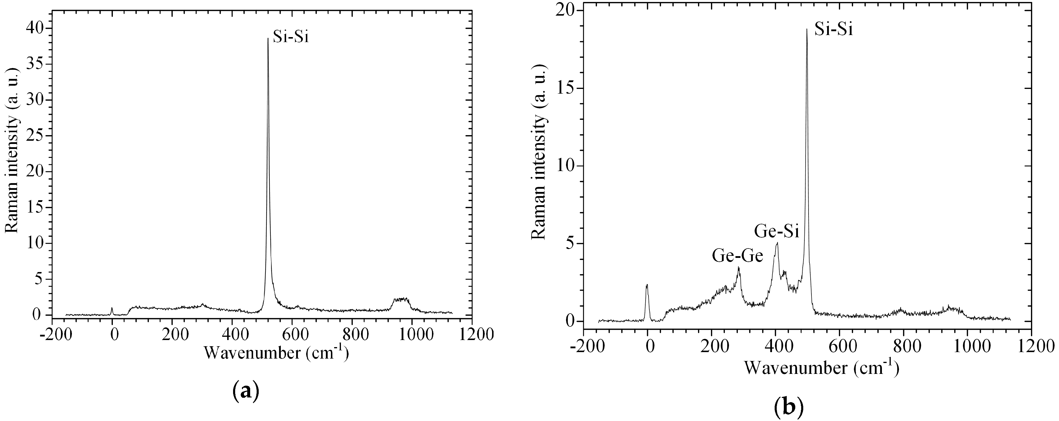
Figure 9a shows a typical spectrum from the UV Raman tests. The 325-nm UV laser can only penetrate the crystal silicon to a depth of ~10 nm, which is similar to the thickness of the strained silicon. Hence, the wavenumber detected by the 325-nm laser achieves a mean wavenumber of 511.98 cm−1 based on results from 66 different sampling spots, which originated solely from the ε-Si layer and were characterized by the average strain and stress of this layer. The residual stress in the ε-Si layer can be treated as a biaxial stress state, with stress components σx = σy = σ and strain components εx = εy = ε, where x and y denote the in-plane directions. According to the Raman-mechanical relationship of C-Si with the (100) crystal plane [28],
ε = 1.204 × 10 3 Δ w σ = 217.28 Δ w   ( MPa ) .
According to Equation (1), ε = −1.204 × 10−3 × (511.98–519.78) = 9.39‰ ≈ 1% and σ = −217.28 × (511.98–519.78) ≈ 1.69 GPa, where wavenumber 519.78 cm−1 was calibrated on a silicon wafer of the same production batch with the ε-Si/GeSi/C-Si samples and on the same day of the measurements above. The results showed that the real in-plane strain in the ε-Si layer was ~1%.
For the Raman measurement on the cross-section with a (110) crystal plane, the applicable Raman-mechanical relationship of (110) C-Si was given as Equation (2), where the residual stress is treated as a uniaxial stress state, because the normal component on the cross-section surface (denoted as σx) was released during the sample preparation, σx = 0, σy = σ and strain components εx = εy = ε, where x and y denote the in-plane directions [28].
ε = 2.58 × 10 3 Δ w σ = 434.58 Δ w   ( MPa ) .
The cross-sectional stress analyses for the Raman data from the sampling spot inside the C-Si layer can use the Raman-mechanical relationship shown as Equation (2), whereas those from the GeSi layers cannot use Equation (2) directly. Figure 9b shows a typical Raman spectrum of the germanium silicon alloy, which includes three major peaks: A Si-Si band at ~500 cm−1, a Ge-Si band at ~400 cm−1 and a Ge-Ge band at ~300 cm−1. If elemental Si dominated the Ge-Si alloy, just like the buffer layers in this work, the Raman peak of the Si-Si band would be strong and sufficiently narrow (shown in Figure 5 and Figure 6) for mechanical measurement. However, Equation (2) is not applicable directly for the Si-Si band of germanium silicon alloy. As shown in Figure 4, the Raman wavenumber decreases sharply inside the GeSi layers, whose increment is up to 14 cm−1, denoting more than 6 GPa by using Equation (2). This is inconsistent with the reality of C-Si or GeSi strength. In fact, due to the influence of phonon confinement, the change in the wavenumber of the Si-Si band in the Raman spectrum of germanium silicon is not only induced by the strain, but also by the influence of phonon confinement. Tsang [29] presented an empirical relationship for the wavenumber wSi-Si, the Ge content x and the strain ε, which is regarded as suitable for the germanium-silicon alloy with 0 < x < 0.25. Meanwhile, the elastic parameters of the germanium–silicon alloy followed the modulus-content linear model proposed by Kasper et al. [30].
C i j = x C i j , Ge + ( 1 x ) C i j , Si , i , j = 1 6 ,
where Cij, Cij,Ge and Cij,Si were components of the elastic coefficient tensors of the Ge-Si alloy, germanium and silicon, respectively. Hence the Raman-mechanical relationship suitable for the stress analysis inside the GeSi layers on the (110) cross-section in this work is given by Equation (4) [11].
σ = ( 100 x 435 ) ( Δ w + 62 x ) ( MPa ) .
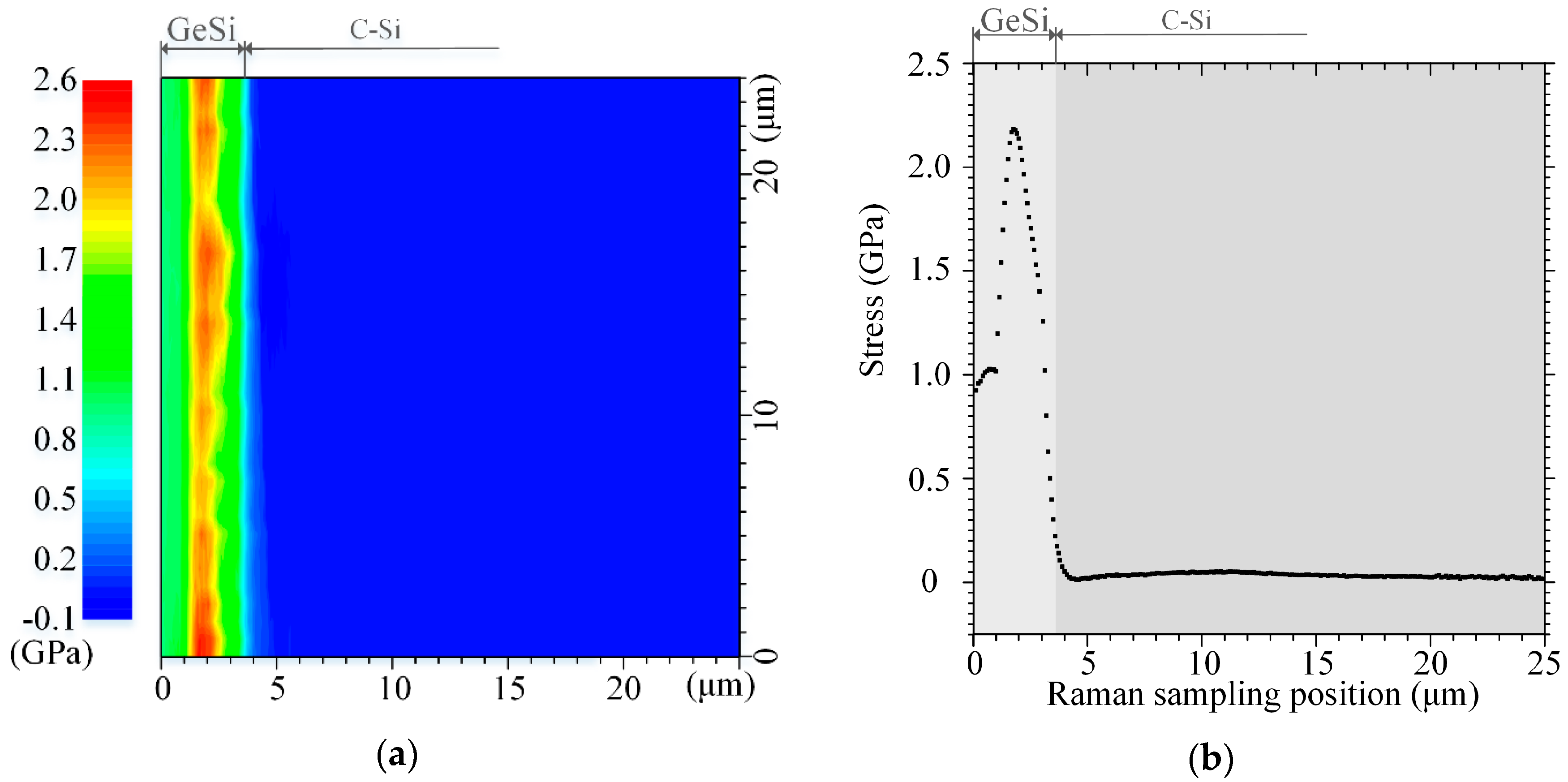
The residual stress distribution along the deepness direction of this multilayer structure is given as Figure 10, where the stress inside the C-Si substrate was achieved by using Equation (2), and that inside the germanium-silicon buffer layers was achieved by using Equation (4). Figure 10 shows that there exists serious residual stress inside the buffer layers. The residual stress increases rapidly in the beginning of the epitaxial growth. The mean stress gradient during the first 2 μm of the graded buffer layer was 777.5 MPa/μm. With further growth of the GexSi1−x layer, the residual stress stopped increasing and then began to decrease, which reduced the stress gradients and even turned them negative, until the beginning of the relaxed buffer layer. In the Ge0.2Si0.8 layer, the residual stress was stable compared with that in the GexSi1−x layer. The mean residual stress in the relaxed buffer layer was ~1.01 GPa.

4. Discussion

The stress distribution achieved by using Raman mapping showed that the residual stress did not increase continuously with the gradual rise in germanium content. The diameter of elemental germanium is larger than that of the silicon, and so is the lattice size of the Ge crystal. In the germanium–silicon layer prepared by reduced-pressure CVE, most silicon maintained its monocrystalline stage according to the Raman FWHM results (shown in Figure 7) and high-resolution TEM image (shown in Figure 7b,d). Therefore, some strain, and hence residual stress, was introduced into the buffer layer. The maximum residual tensile stress introduced by doping Ge in Si was 2.2 GPa, which did not induce any visible break or crack in each layer or interface, because of the birth and propagation of the dislocation, which was coincident with the GeSi alloy growth. Dislocation networks and dislocation loops helped to release the residual stress induced by the change in lattice dimension during the growth of a graded buffer layer where the germanium content increased gradually, which was positive for the reliability and stability of the ε-Si structure during its application.
In the GexSi1−x layer, the germanium component started from zero at the GexSi1−x/C-Si interface and increased with a linear gradient (shown in Figure 3a), which resulted in a gradual change in lattice constant, avoided a sudden difference in lattice constant at the interface and reduced the mismatch strain and dislocation nucleation density compared with other growth methods. When the epitaxial GexSi1−x layer grew accompanied by a linear increase in Ge content, the mismatch strain relaxed gradually, and slowed down the extent of dislocation lines and the formation of dislocation networks. The dislocation lines stopped when the strain energy was released, which made the dislocation networks limited inside the GexSi1−x layer and unable to extend into the Ge0.2Si0.8 and ε-Si. Thus, the growth of the gradient-graded component can be effective for confining dislocations within the buffer layer.
As shown by the Raman results, the residual stress remained stable and the lattice quality improved inside the relaxed buffer layer. No obvious dislocation existed in this layer in the TEM images. These results proved that it was helpful to reduce the negative effect of germanium, and to improve the liability and performance of the microdevice based on strained-silicon technology.

5. Conclusions

In this work, multiscale structural and mechanical properties of a ε-Si/GeSi/C-Si material were investigated by several experimental methods. Based on sample cross-sections, the components and thickness of each layer were measured by EDS and SEM and the crystal and lattice characteristics and quality were observed by TEM and MRS. The residual stress distribution inside this multilayer material was achieved through micro-Raman mapping. The experimental results showed that the residual stress introduced during the heteroepitaxial growth was effectively controlled inside the buffer layers within a safe magnitude. The twin (graded plus relaxed) GeSi alloy structure provided a stable and reliable buffer for the manufacture of a strained-silicon film/ribbon in microelectronic devices.

Author Contributions

Conceptualization, W.Q. and Y.-S.Z.; methodology, W.Q., H.-T.W. and Y.-C.Z.; validation, L.-L.M.; resources, R.-R.L.; data curation, L.-L.M.; writing—original draft preparation, W.Q.; writing—review and editing, W.Q. and Y.-S.Z.

Funding

This research was funded by the National Key Research and Development Program of China (2018YFB0703500) and the National Natural Science Foundation of China (Grant Nos. 11827802, 11772223 and 11772227).

Acknowledgments

We thank Yongfeng Lu from the University of Nebraska-Lincoln for providing the experimental facilities, Dawei Li from the University of Nebraska-Lincoln for the AFM and WLI tests, and Laura Kuhar, from Liwen Bianji, Edanz Group China (www.liwenbianji.cn/ac), for editing the English text of a draft of this manuscript.

Conflicts of Interest

The authors declare no conflict of interest.

References

  1. Roldan, R.; Castellanos-Gomez, A.; Cappelluti, E.; Guinea, F. Strain engineering in semiconducting two-dimensional crystals. J. Phys. Condens. Matter 2015, 27, 313201. [Google Scholar] [CrossRef] [PubMed] [Green Version]
  2. Cao, T.; Wang, D.; Geng, D.S.; Liu, L.M.; Zhao, J. A strain or electric field induced direct bandgap in ultrathin silicon film and its application in photovoltaics or photocatalysis. Phys. Chem. Chem. Phys. 2016, 18, 7156–7162. [Google Scholar] [CrossRef] [PubMed]
  3. Saran Yalamarthy, A.; Senesky, D.G. Strain- and temperature-induced effects in AlGaN/GaN high electron mobility transistors. Semicond. Sci. Technol. 2016, 31, 035024. [Google Scholar] [CrossRef] [Green Version]
  4. Dzuba, J.; Vanko, G.; Babchenko, O.; Lalinský, T.; Horvát, F.; Szarvas, M.; Kováč, T.; Hučko, B. In Strain induced response of AlGaN/GaN high electron mobility transistor located on cantilever and membrane. Int. Conf. Adv. Semicond. Devices Microsyst. 2017, 227–230. [Google Scholar] [CrossRef]
  5. Shen, T.; Penumatcha, A.V.; Appenzeller, J. Strain Engineering for Transition Metal Dichalcogenides Based Field Effect Transistors. ACS Nano 2016, 10, 4712. [Google Scholar] [CrossRef] [PubMed]
  6. Wen, H.; Borlaug, D.; Wang, H.; Ji, Y.; Jalali, B. Engineering Strain in Silicon Using SIMOX 3-D Sculpting. IEEE Photonics J. 2016, 8, 1–9. [Google Scholar] [CrossRef]
  7. Tian, P.; Edwards, P.R.; Wallace, M.J.; Martin, R.W.; McKendry, J.J.D.; Gu, E.; Dawson, M.D.; Qiu, Z.-J.; Jia, C.; Chen, Z.; et al. Characteristics of GaN-based light emitting diodes with different thicknesses of buffer layer grown by HVPE and MOCVD. J. Phys. D Appl. Phys. 2017, 50, 075101. [Google Scholar] [CrossRef] [Green Version]
  8. Kaganer, V.M.; Jenichen, B.; Ramsteiner, M.; Jahn, U.; Hauswald, C.; Grosse, F.; Fernández-Garrido, S.; Brandt, O. Quantitative evaluation of the broadening of x-ray diffraction, Raman, and photoluminescence lines by dislocation-induced strain in heteroepitaxial GaN films. J. Phys. D Appl. Phys. 2015, 48, 385105. [Google Scholar] [CrossRef]
  9. Lin, T.; Wang, F.; Cheng, C.-H.; Chen, S.; Feng, Z.C.; Lin, G.-R. Strain-related recombination mechanisms in polar InGaN/GaN MQWs on amorphous SixC1-x buffers. Opt. Mater. Express 2018, 8, 1100. [Google Scholar] [CrossRef]
  10. Guo, Q.L.; Di, Z.F.; Lagally, M.G.; Mei, Y.F. Strain engineering and mechanical assembly of silicon/germanium nanomembranes. Mater. Sci. Eng. R 2018, 128, 1–31. [Google Scholar] [CrossRef]
  11. Qiu, W.; Cheng, C.L.; Liang, R.R.; Zhao, C.W.; Lei, Z.K.; Zhao, Y.C.; Ma, L.L.; Xu, J.; Fang, H.J.; Kang, Y.L. Measurement of residual stress in a multilayer semiconductor heterostructure by micro-Raman spectroscopy. Acta Mech. Sin. 2016, 32, 805–812. [Google Scholar] [CrossRef]
  12. Lockwood, D.J.; Wu, X.; Baribeau, J.M.; Mala, S.A.; Wang, X.; Tsybeskov, L. Si/SiGe Heterointerfaces in One-, Two-, and Three-Dimensional Nanostructures: Their Impact on SiGe Light Emission. Front. Mater. 2016, 3. [Google Scholar] [CrossRef]
  13. Cen, H.; Kang, Y.L.; Lei, Z.K.; Qin, Q.H.; Qiu, W. Micromechanics analysis of Kevlar-29 aramid fiber and epoxy resin microdroplet composite by Micro-Raman spectroscopy. Compos. Struct. 2006, 75, 532–538. [Google Scholar] [CrossRef]
  14. Wang, M.; Hu, X.F.; Wu, X.P. Internal microstructure evolution of aluminum foams under compression. Mater. Res. Bull. 2006, 41, 1949–1958. [Google Scholar] [CrossRef]
  15. Li, X.; Peng, Y. Investigation of capillary adhesion between the microcantilever and the substrate with electronic speckle pattern interferometry. Appl. Phys. Lett. 2006, 89, 234104. [Google Scholar] [CrossRef]
  16. Li, X.D.; Su, D.C.; Zhang, Z. A novel technique of microforce sensing and loading. Sens. Actuators A Phys. 2009, 153, 13–23. [Google Scholar] [CrossRef]
  17. Stoney, G.G. The Tension of Metallic Films Deposited by Electrolysis. Proc. R. Soc. Lond. 1909, 82, 40–43. [Google Scholar] [CrossRef]
  18. Van, A.S.; Batenburg, K.J.; Rossell, M.D.; Erni, R.; Van, T.G. Three-dimensional atomic imaging of crystalline nanoparticles. Nature 2011, 470, 374–377. [Google Scholar] [CrossRef] [Green Version]
  19. Nawaz, A.; Mao, W.G.; Lu, C.; Shen, Y.G. Mechanical properties, stress distributions and nanoscale deformation mechanisms in single crystal 6H-SiC by nano-indentation. J. Alloys Compd. 2017, 708, 1046–1053. [Google Scholar] [CrossRef]
  20. Qiu, W.; Li, Q.; Lei, Z.K.; Qin, Q.H.; Deng, W.L.; Kang, Y.L. The use of a carbon nanotube sensor for measuring strain by micro-Raman spectroscopy. Carbon 2013, 53, 161–168. [Google Scholar] [CrossRef]
  21. Kang, Y.L.; Qiu, Y.; Lei, Z.K.; Hu, M. An application of Raman spectroscopy on the measurement of residual stress in porous silicon. Opt. Laser Eng. 2005, 43, 847–855. [Google Scholar] [CrossRef]
  22. Qiu, W.; Kang, Y.L. Mechanical behavior study of microdevice and nanomaterials by Raman spectroscopy: A review. Sci. Bull. 2014, 59, 2811–2824. [Google Scholar] [CrossRef]
  23. Zhao, C.; Wen, S.; Hou, Q.; Qiu, W.; Xing, Y.; Su, S.; Cheng, B. Strain status of epitaxial Ge film on a Si (001) substrate. J. Phys. Chem. Solids 2016, 90, 87–92. [Google Scholar] [CrossRef]
  24. Liang, R.; Zhang, T.; Wang, J.; Xu, J. High-Resolution Light-Emitting Diode Array Based on an Ordered ZnO Nanowire/SiGe Heterojunction. IEEE Trans. Nanotechnol. 2016, 15, 539–548. [Google Scholar] [CrossRef]
  25. Shubhakar, K.; Bosman, M.; Neucheva, O.A.; Loke, Y.C.; Raghavan, N.; Thamankar, R.; Ranjan, A.; O’Shea, S.J.; Pey, K.L. An SEM/STM based nanoprobing and TEM study of breakdown locations in HfO2/SiOx dielectric stacks for failure analysis. Microelectron. Reliab. 2015, 55, 1450–1455. [Google Scholar] [CrossRef]
  26. Zhao, C.W.; Xing, Y.M.; Zhou, C.E.; Bai, P.C. Experimental examination of displacement and strain fields in an edge dislocation core. Acta Mater. 2008, 56, 2570–2575. [Google Scholar] [CrossRef]
  27. De Wolf, I. Relation between Raman frequency and triaxial stress in Si for surface and cross-sectional experiments in microelectronics components. J. Appl. Phys. 2015, 118, 053101. [Google Scholar] [CrossRef]
  28. Qiu, W.; Ma, L.L.; Li, Q.; Xing, H.D.; Cheng, C.L.; Huang, G.Y. A general metrology of stress on crystalline silicon with random crystal plane by using micro-Raman spectroscopy. Acta Mech. Sin. 2018. [Google Scholar] [CrossRef]
  29. Tsang, J.C.; Mooney, P.M.; Dacol, F.; Chu, J.O. Measurements of alloy composition and strain in thin GexSi1−x layers. J. Appl. Phys. 1994, 75, 8098–8108. [Google Scholar] [CrossRef]
  30. Dismukes, J.P.; Ekstrom, L.; Paff, R.J. Lattice Parameter and Density in Germanium-Silicon Alloys. J. Phys. Chem. 1964, 68, 3021–3027. [Google Scholar] [CrossRef]
Figure 1. (a) Schematic structure of prepared ε-Si/GeSi/C-Si material, (b) scanning-electron microscopy (SEM) image of multilayer vicinity of sample cross-section. CVE, chemical vapor epitaxy.
Applsci 08 02333 g001
Figure 2. The surface roughness of cross-sectional surface measured by (a) atomic-force microscope (AFM) and (b) white-light interferometer.
Applsci 08 02333 g002
Figure 3. Elemental distribution along the depth direction achieved by using energy-dispersive spectroscopy (EDS).
Applsci 08 02333 g003
Figure 4. (a) Si-Si band wavenumber image obtained by Raman mapping on the sample cross-section, (b) wavenumber distribution along the depth direction.
Applsci 08 02333 g004
Figure 5. (a) Si-Si band Raman-intensity image obtained by Raman mapping on the sample cross-section, (b) Raman-intensity distribution along the depth direction.
Applsci 08 02333 g005
Figure 6. (a) Si-Si band full-width-at-half-maximum (FWHM) image obtained by Raman mapping on the sample cross-section, (b) FWHM distribution along the depth direction.
Applsci 08 02333 g006
Figure 7. High-resolution transmission-electron microscopy (TEM) images of sample cross-section (a) at the ε-Si and Ge0.2Si0.8 layers, (b) inside the Ge0.2Si0.8 layer, (c) at the Ge0.2Si0.8/GexSi1−x interface and (d) inside the GexSi1−x layer.
Applsci 08 02333 g007aApplsci 08 02333 g007b
Figure 8. Low-resolution TEM images of sample cross-section (a) around Ge0.2Si0.8 layer, (b,c) at GexSi1−x/C-Si interface and (d) inside GexSi1−x layer with a dislocation loop.
Applsci 08 02333 g008
Figure 9. Raman spectra of (a) strained silicon (surface) and (b) germanium-silicon (cross-section).
Applsci 08 02333 g009
Figure 10. (a) Distribution image of residual stress on sample cross-section, (b) mean residual stress along the depth direction.
Applsci 08 02333 g010

