1. Introduction
Filters occupy a key place in microwave communication systems. Their roles include suppression of unwanted signals or isolation of certain parts of a system. There is a demand to develop compact, efficient and low cost filters, for which substrate integrated waveguide (SIW) technology [
1] offers a good compromise between high performance but bulky waveguides and compact planar lines such as microstrip. SIW technology was first implemented on classic Printed Circuit Board (PCB) [
2], then on ceramic substrates, for which laser cutting or drilling is necessary [
3,
4]. In this paper, we present SIW filters based on cyclo-olefin polymers (COP). The goal was to combine high and low thicknesses to associate high quality factor cavities with microstrip accesses compatible with monolithic microwave integrated circuits (MMIC). The objective is to minimize the length of the bonding wires between the components, allowing an optimal integration of the filter in a global system. Cyclo-olefin polymers offer many interesting properties for the design of microwave passive devices in the millimeter wave range. First, their permittivity is low and very stable over a large frequency range and their dielectric losses are very low, even at high frequencies. They have been used for antenna applications [
5] and even for terahertz applications [
6].
When designing conventional SIW passive devices, one of the main limitations is the substrate height, which conditions their electrical performance and compatibility with the other components of the system. This limitation leads to the need to find a compromise. To overcome this constraint, we propose the innovative solution of using a material compatible with a standard molding process. Molding the device makes it possible to vary its thickness between different zones, therefore achieving a higher quality factor in the thicker part and 50 Ω microstrip lines in the thinner access parts. Once the dielectric structure is molded, the laser direct structuring (LDS) technique is used to selectively activate the piece before using an autocatalysis bath to metalize the LDS zones. Just before the metallization steps, we use mechanical drillings to make a set of via holes, defining the expected electrical response.
The aim of this paper is to show that it is possible to build high performance millimeter wave filters with COP by combining molding, mechanical drilling and 3D laser direct structuring metallization. The paper is organized as follows: In the first part, we present the main particularities of the chosen COP and the benefits of using them to design millimeter resonant cavities. Then, we present the design steps taken to realize two bandpass filters.
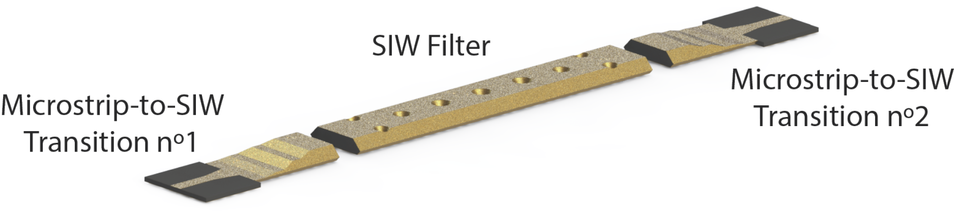
Figure 1 presents the exploded view of the proposed topology divided in two different parts: The SIW inductive post filter core, and two transitions with planar microstrip access. As each part was designed independently, we present the ideal filter synthesis, the manufacturing specifications to be taken into account, and the design of the transition in turn. The microstrip-to-SIW transition is designed to work over a wide bandwidth. We conceived two narrow-band filters (w < 10%), to obtain a good dynamic for the evaluation of the insertion losses (IL), and thus of the quality factors of the cavities. Finally, we present the experimental data and compare them with simulations. In choosing a central frequency of around 38 GHz for the filters, the goal was to demonstrate the efficiency up to millimeter frequency range of the selected thermoplastics coupled with industrial technologies.
For the design of millimeter SIW filters, it must be mentioned that other materials can be used. To our knowledge, the solutions realized with RO5880 are state-of-the-art [
7]. At the end of the paper, our results are compared with such solutions [
7,
8]. Due to their very good electrical properties at very high frequency, benzocyclobutene (BCB) and liquid crystal polymer (LCP) are also considered by some authors. In References [
9,
10], Ku-band SIW BCB filters with embedded silicon vias and K-band LCP SIW filters, respectively, are presented. However, despite interesting performances, these solutions use planar substrates with low thickness between 100 and 400 μm, leading to limited quality factors. Low Temperature Co-fired Ceramic (LTCC) is also a very convenient solution to minimize the footprint and to provide new freedom degrees in the design. Very interesting filters, designed at 60 GHz, are presented in Reference [
11], but once again present limited quality factors, below 100.
2. Thermoplastics and SIW Filters
Cyclo-olefin polymers or copolymers (COP/COC) have excellent optical and microwave characteristics and are widely used in a broad range of applications, including packaging of films, lenses, displays, and medical devices. They also offer other chemical and physical advantages, and are low in cost. Topas® (Frankfurt-Höchst, Germany), Mitsui Chemicals® (Tokyo, Japan), Arton® (Tokyo, Japan), and Zeon® (Tokyo, Japan) are the main manufacturers. Among these, Zeon® was the first to propose a COP, RS420-LDS, compatible with the LDS metallization technique under patent and commercialized by the company LPKF®.
To make it possible to exploit this property, a pure COP is loaded with organometallic particles, which implies some changes to the electrical and optical properties. Inevitably, the dielectric losses increase slightly, and the materials become opaque and fully black, hence changing the optical properties of the polymer.
Table 1 compares the dielectric permittivity and loss tangent of the loaded COP RS420-LDS with the conventional COP 480R. In [
12], we used a cavity-perturbation method and a Ka-band waveguide method to extract dielectric properties, at 7 GHz and in the 26–40 GHz frequency band respectively. The accuracy of waveguide method is known to be too low to extract loss tangent values lower than 10
−3. However, both methods give similar values of permittivity from 7 to 40 GHz.
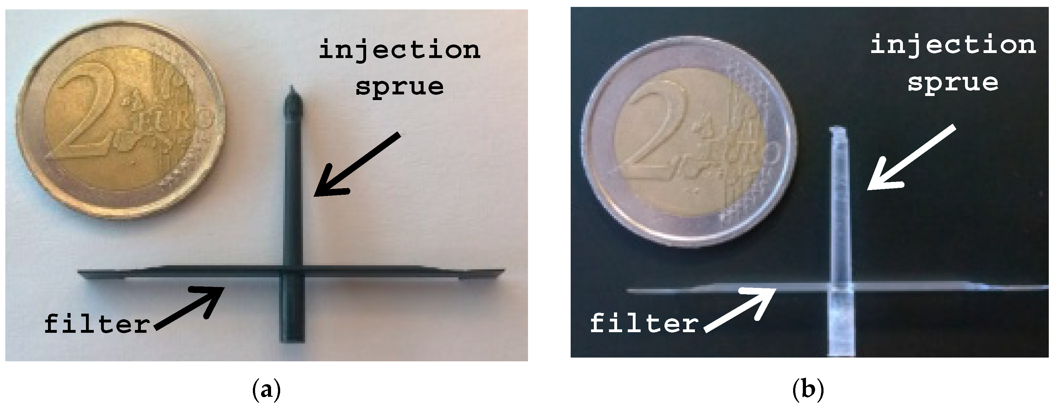
To illustrate the difference in appearance,
Figure 2 shows pictures of the two filters after molding and before drilling. The black and the transparent filters are the loaded and the conventional, and are respectively presented in
Figure 2a,b. Each picture is a side view of the filter, showing the vertical injection sprue which must be suppressed.
As the electromagnetic fields are entirely confined in the dielectric, the loss tangent is a significant parameter for the development of SIW filters.
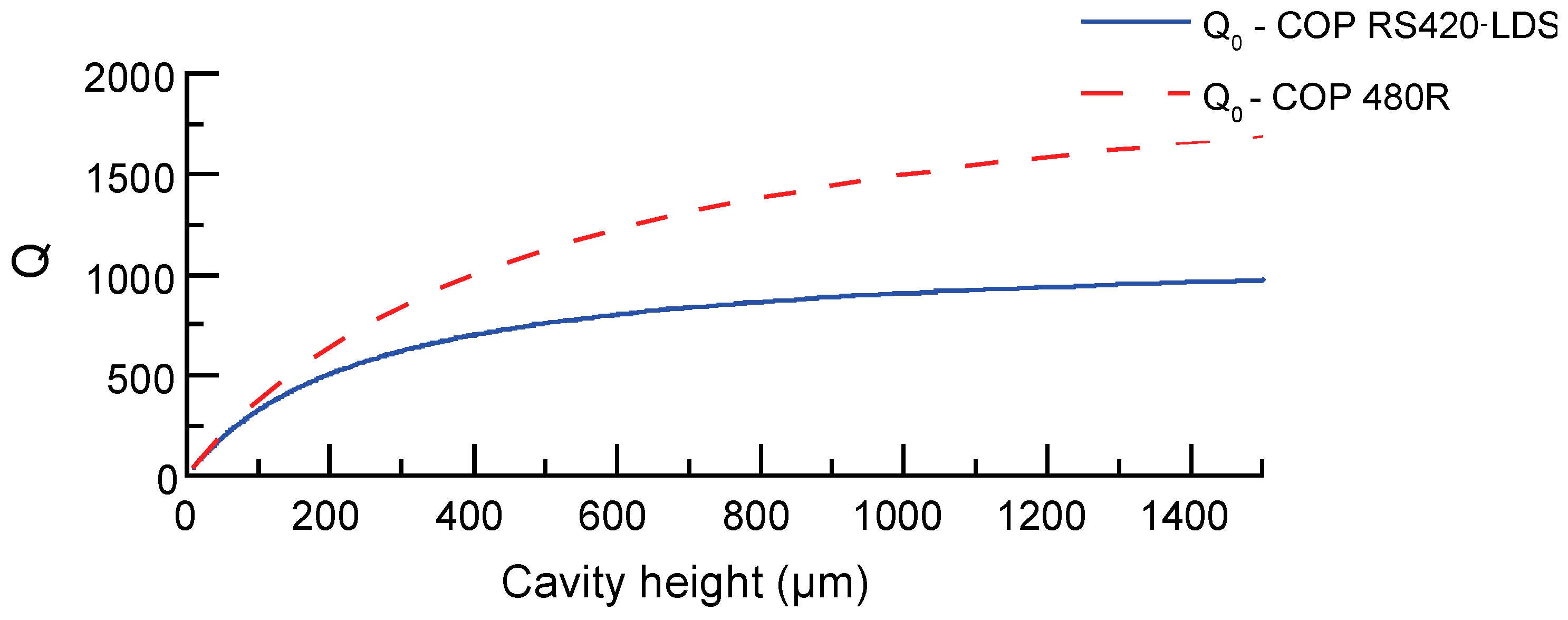
Figure 3 shows (in blue) the evolution at 38 GHz of the unloaded quality factor of a parallelepiped cavity for a TE101 resonant mode in COP RS420-LDS substrate. The Q factor increases significantly with the height of the cavity. We also plotted the same curve for COP RS420-LDS (in red), in order to show the impact of a better loss tangent. Indeed, the curves are limited by the value of the dielectric quality factor (Qd), equal to 1/tan δ. For COP RS420-LDS and COP 480R, the values of Qd are around 1300 and 3000, respectively. Therefore, this encourages developing filters on low loss material with high thickness substrates. The limit is to avoid a resonant mode other than the desired one appearing in the cavity.
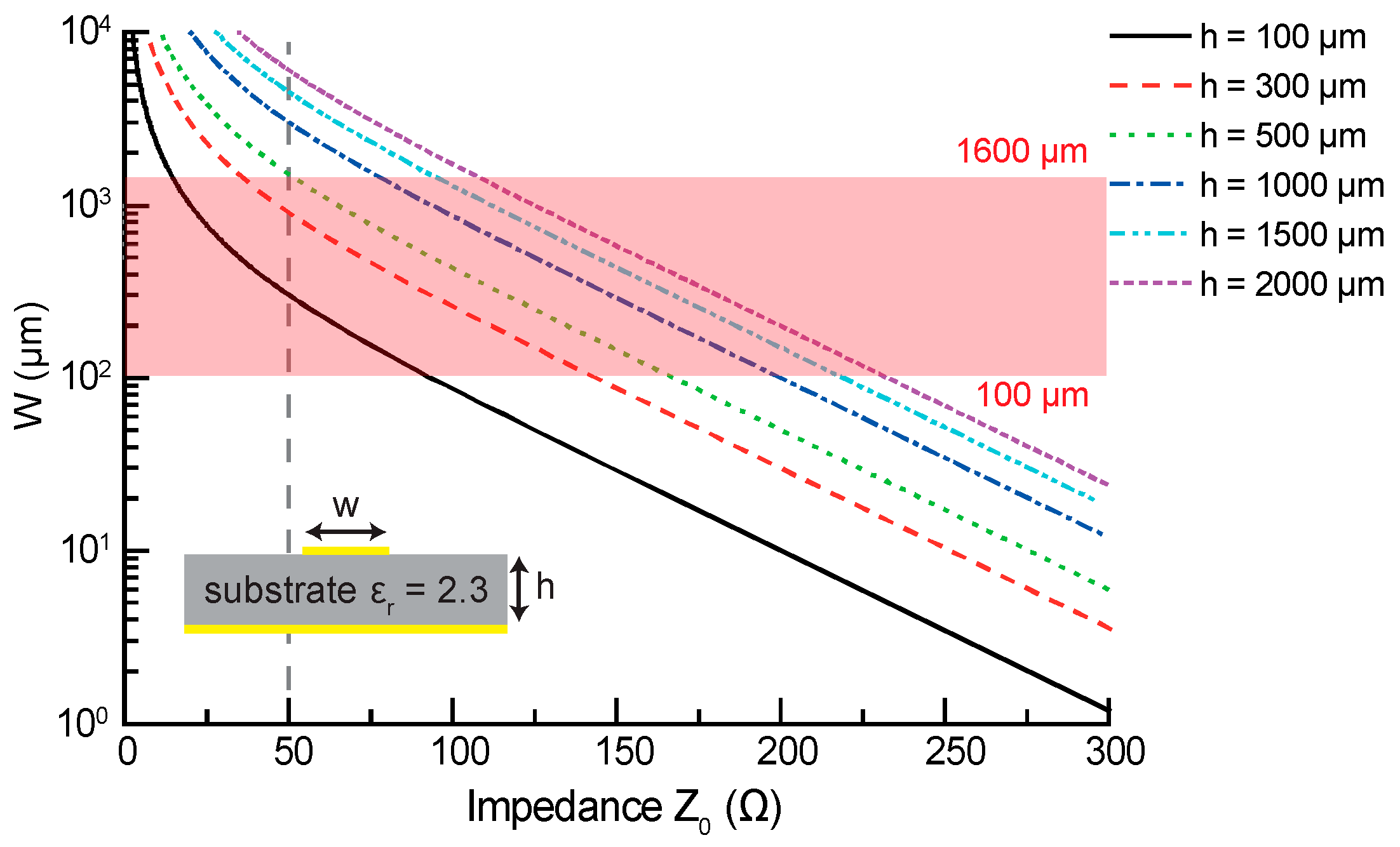
Figure 4 shows the width of microstrip line against characteristic impedance, calculated for a permittivity of 2.3, for the COP 480R. As the dielectric constants of the two materials are not very different, 2.3 against 2.48, very similar values and conclusions would be obtained and drawn for the COP RS420-LDS. Depending on the substrate characteristics (height, permittivity, metallization limitations), some line impedances can be correctly realized and others not. For our 38 GHz filters, the width of the microstrip-line must be between 100 μm and 1600 μm. The lower bound, equal to 100 μm, was chosen to limit the sensitivity to technological dispersions when using the LDS technique for metallization. The higher bound, equal to 1600 μm, is the limitation due to our chosen in-out connector. Moreover, it is important for us to limit the width of our microstrip lines to avoid discontinuity effects as much as possible. As we see in
Figure 4, only heights below 500 μm allowed us to obtain a 50 Ω line impedance while also limiting the Q factor. The problem can be solved through molding techniques, allowing a 3-dimensional transition to be built between the low thickness microstrip parts, with the high thickness cavities constituting the heart of the filter. Compared with previous work carried out in our laboratory [
3,
4], the possibility of modulating the thickness offers new opportunities in terms of electrical performances, since we are able to design an efficient microstrip-to-SIW transition.
3. Filter Design
3.1. Filter Synthesis
The SIW filter is obtained by forming cavities inside the substrate, and coupled by inductive posts, whose equivalent models were presented by Marcuvitz [
13]. The synthesis is fully described in chapter eight of Reference [
14]. Previous inductive post filters have been built in our laboratory using other materials [
3,
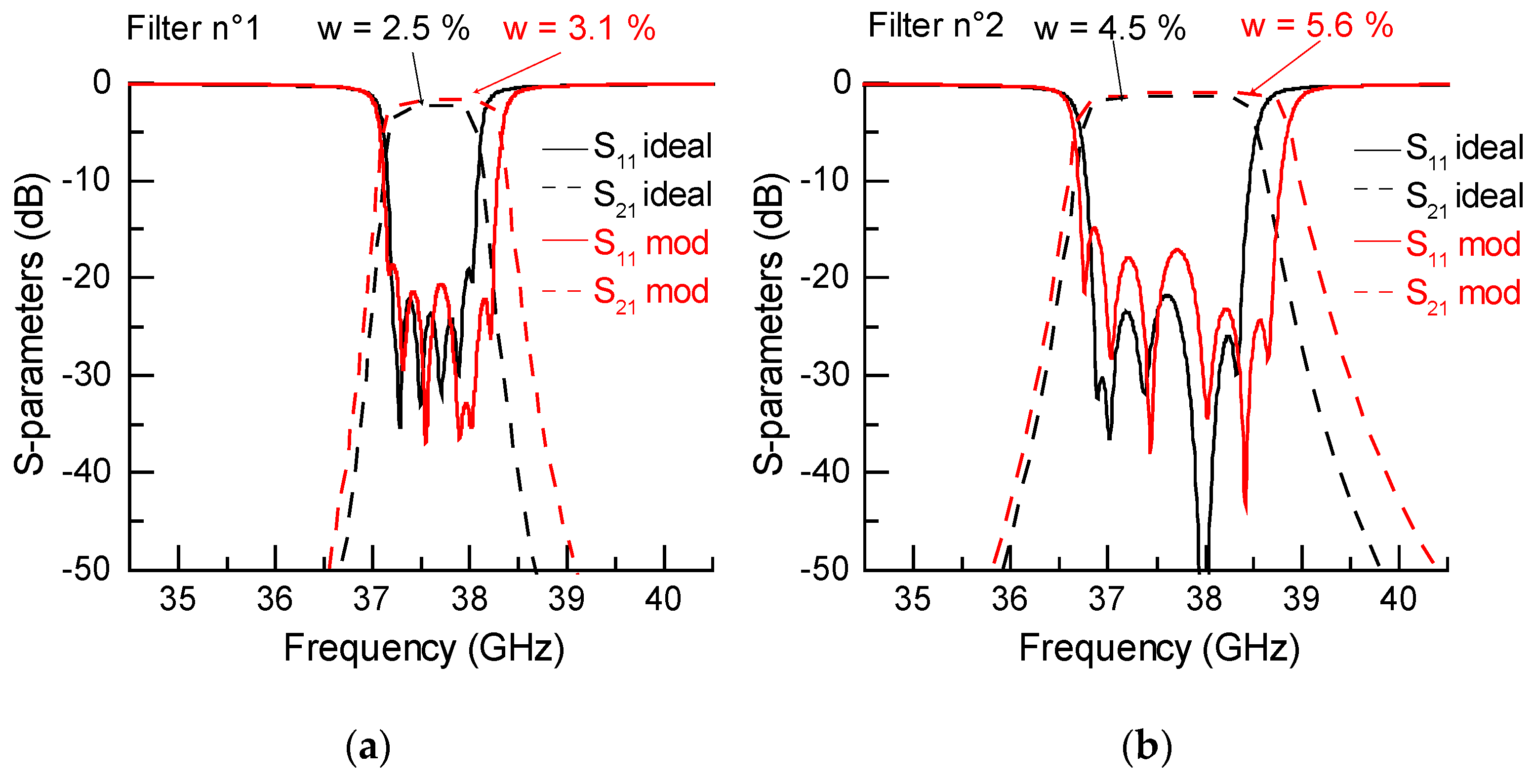
4]. Here we chose a six-pole Chebyshev SIW filter with a narrow relative bandwidth, under 10%. This filter operates at 37.5 GHz and we synthesized two electrical responses with relative bandwidths 2.5% and 4.5%, respectively. The order of the filter is arbitrary. It was chosen at six, in order to be sufficiently representative in our demonstration.
3.2. Manufacturing Specifications
A thermoplastic of this type cannot withstand high temperatures. For example, the glass transition temperature of COP RS420-LDS is 136 °C. For this reason, low temperature selective metallization techniques were needed. The one used here was laser direct structuring (LDS), under patent and commercialized by the company LPKF.
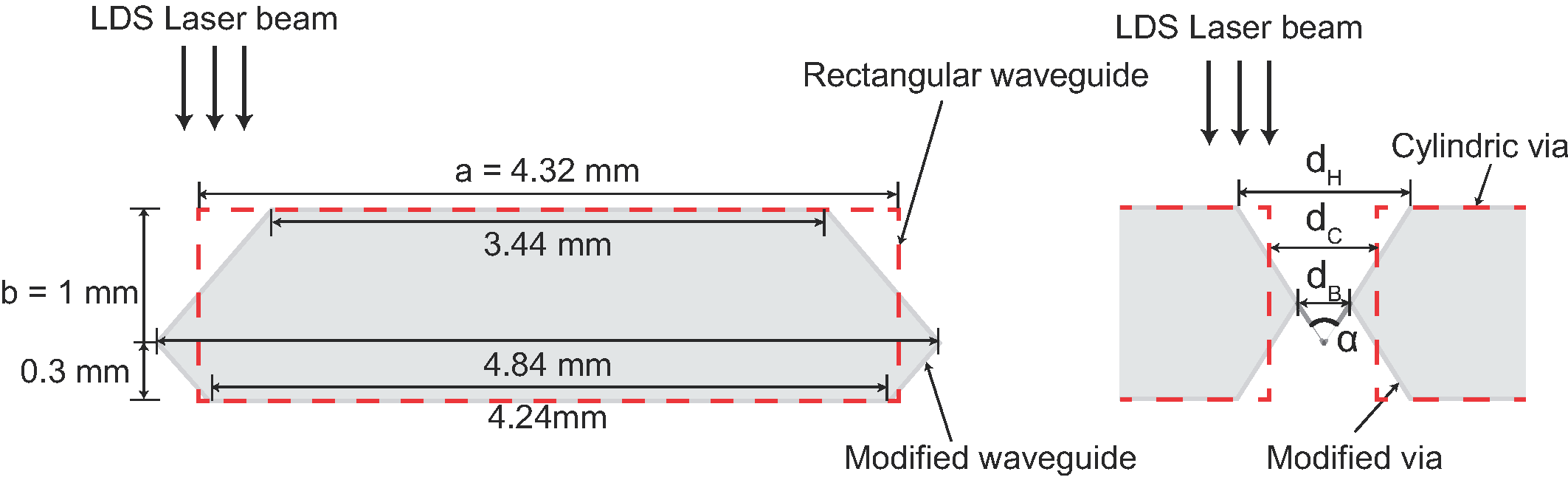
The principle is to activate the substrate locally, using a laser beam. The COP RS420-LDS used here, loaded with additional organometallic particles, permits the activation, and subsequently the electroless metal deposition, of the activated surfaces. The addition of the particles to the polymer modifies some of the characteristics of the material. It becomes fully black. In addition, the relative dielectric permittivity and the dielectric losses increase. One constraint of this technique is that it does not allow vertical walls to be activated. We thus had to rework the shape of walls and vias. We substituted cylindrical vias with hourglass shaped vias, which had an alpha angle of 70°.
The molding process also has its own specifications. One of these is the capability of the injection press to correctly fill the entire mold, especially in low thickness areas. In fact, the structure is easier to mold with low relative differences of thickness.
To better fit with standard MMIC dimensions, with which the filter could be interfaced in a system, we chose an access thickness of 300 μm. Moreover, the injection mold is in two parts, creating a surface joint, which has to be kept at the same height as the access line. To illustrate the overall changes,
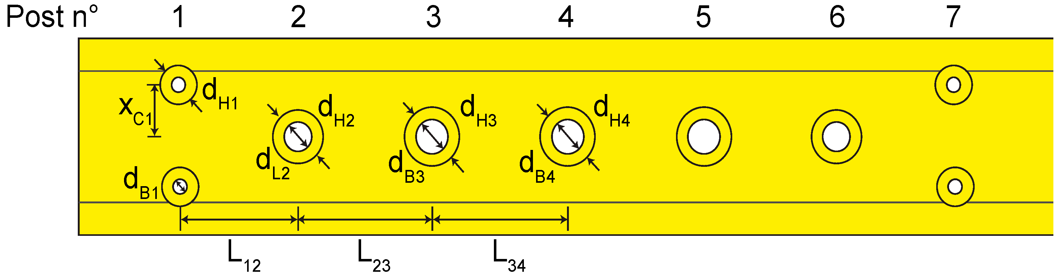
Figure 5 compares the modified filter with inclined walls (in grey) with the traditional rectangular SIW (in dotted red lines). Moreover, all the shape modifications were made, taking care to keep the same resonant modes and, obviously, the same electrical response. The diameters of the inductive posts depend on the electrical requirements and also the characteristics of the waveguide. One critical point here was the diameters of posts 1 and 7, at the extremities of the filter, which were too tiny to be drilled. To overcome this issue, one solution is to substitute each of these posts with a pair of posts, as shown in
Figure 6.
All these technological requirements inevitably modify the electrical response of the filter, and require the structure to be re-adjusted in order to retrieve the original electrical response given by an ideal rectangular SIW filter. The work of re-adjustment of the electrical response is necessarily made with the commercial electromagnetic software ANSYS HFSS. Without any experience, this can be time consuming and it is not easy to obtain exactly the same response. Some differences, such as modification of the bandwidth, can be difficult to eliminate. In this case, the problem needs to be foreseen when designing the prototype. This work was done for the modified SIW filters in our study (dimensions given in
Table 2). The responses of the two filters with relative bandwidths of 2.5% and 4.5%, before and after modifications, are shown in
Figure 7a,b, respectively. As mentioned above, we can obviously observe a slight increase of the bandwidth, but it is important to note that the insertion losses in both cases remain nearly unchanged, meaning that the quality factor was not significantly impacted by the technological modifications. The next step is to design a low loss microstrip-to-waveguide transition.
3.3. Tapered Transition Design
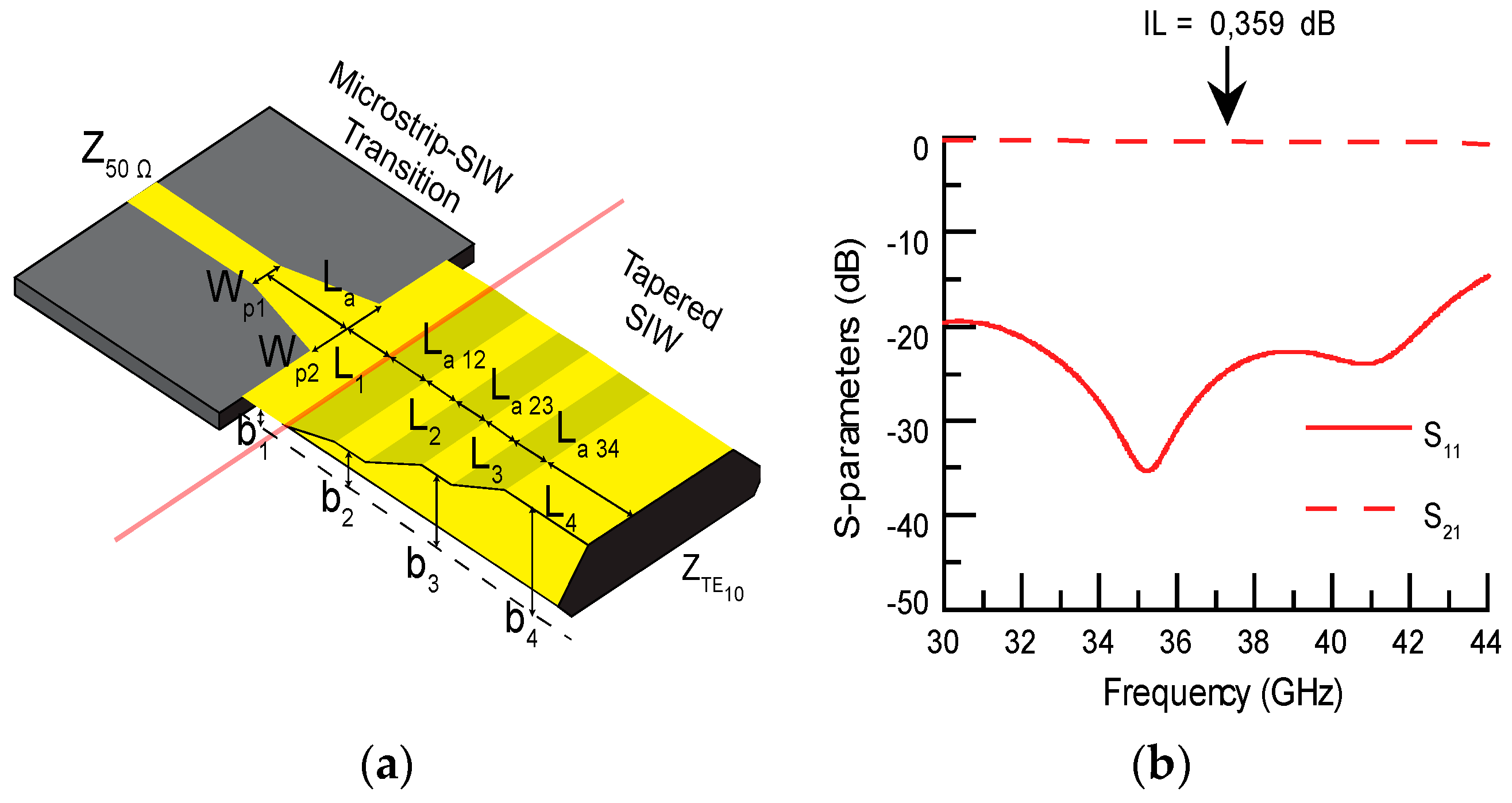
We broke down the transition into two parts. The first one, considering the same thickness of 300 μm, connects the microstrip line to a waveguide via a taper line [
1]. The second part is a waveguide transition, inspired by Reference [
13], on which several regular steps are made from the extremity of the last planar transition to reach a thickness of 1 mm. A good choice of shape of the transition is a key point to ensure correct modal transformation between microstrip TEM and TE10 SIW modes, and vice versa. However, a phase of optimization with an electromagnetic simulator was necessary to correctly adjust all the dimensions in order to obtain a sufficient bandwidth while minimizing insertion losses. The shape of the transition is displayed in
Figure 8a, and the dimensions are given in
Table 3. The electrical response of the transition, given in
Figure 8b, shows a 20 dB relative bandwidth better than 30%, for a central level of insertion losses better than 0.4 dB. It is important to note that, once it is designed, the transition is transparent whatever the filter chosen. This means that the assembly of the whole structure, one filter and two transitions, does not require any modifications.
4. Simulations and Results
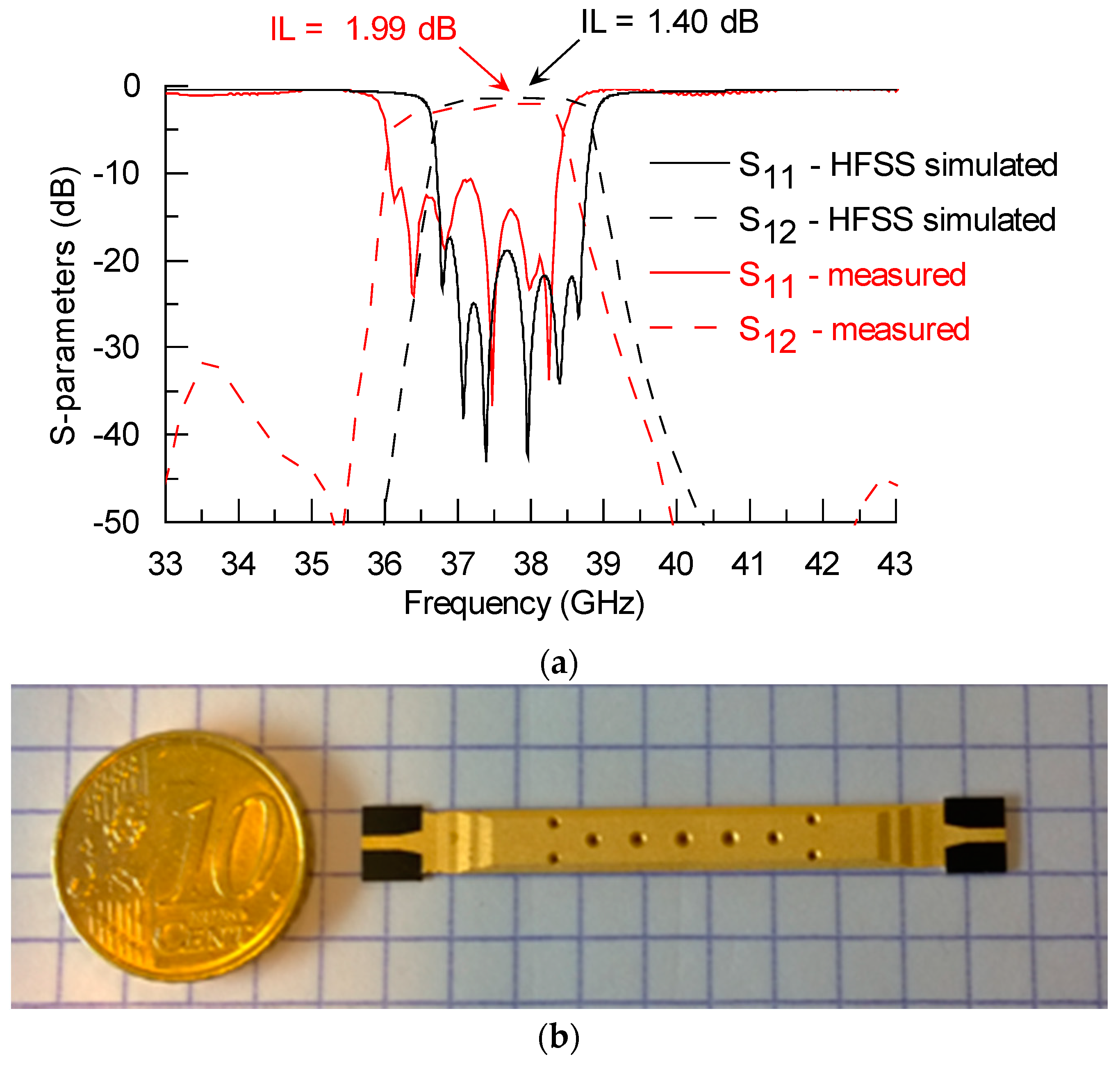
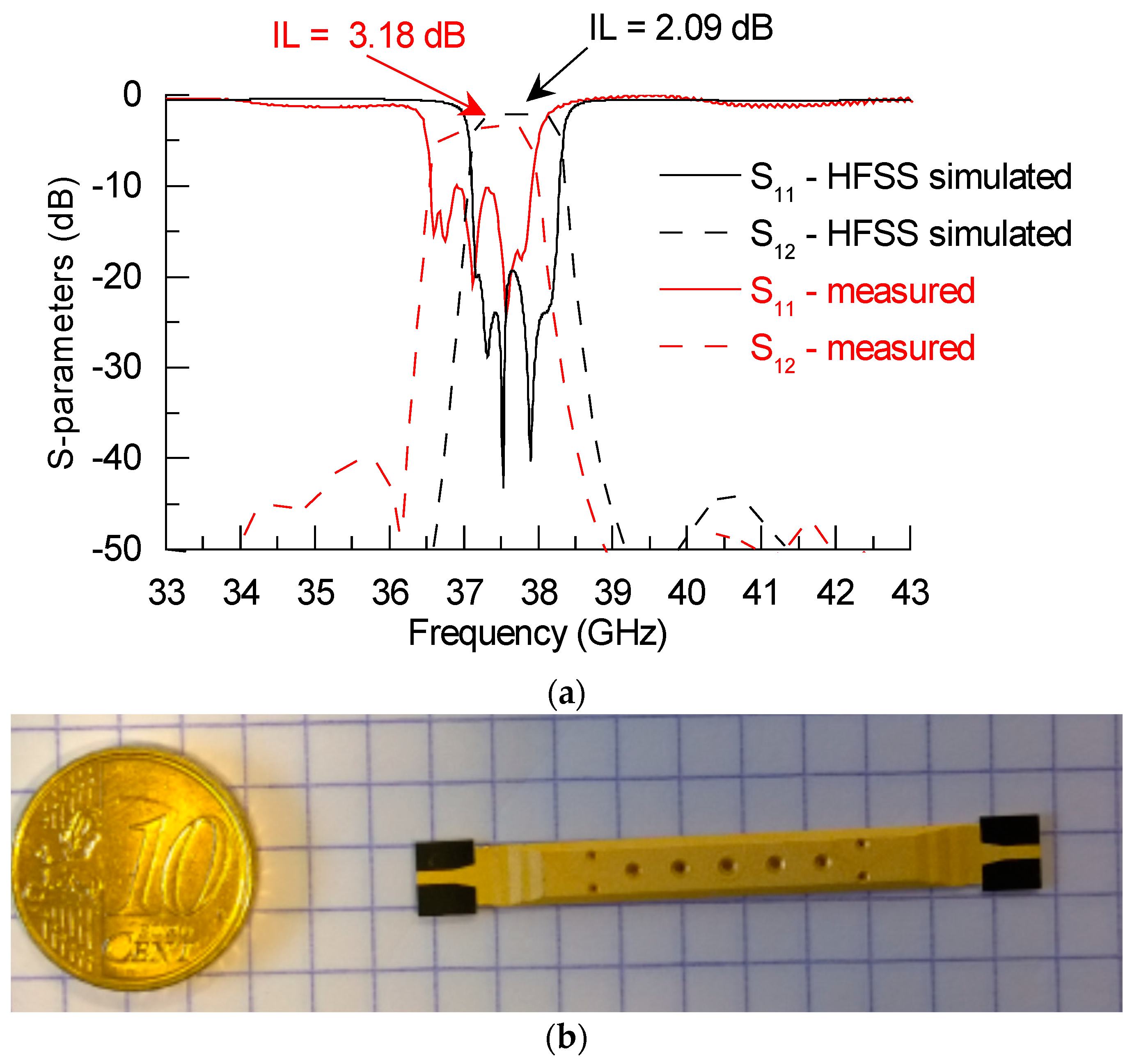
The prototypes of the two filters were built by the French technical center Innovation Plasturgie Composites [
15], which has all the necessary facilities to perform molding, machining and laser direct structuring for metallization. The two prototype filters are presented in
Figure 9b and
Figure 10b.
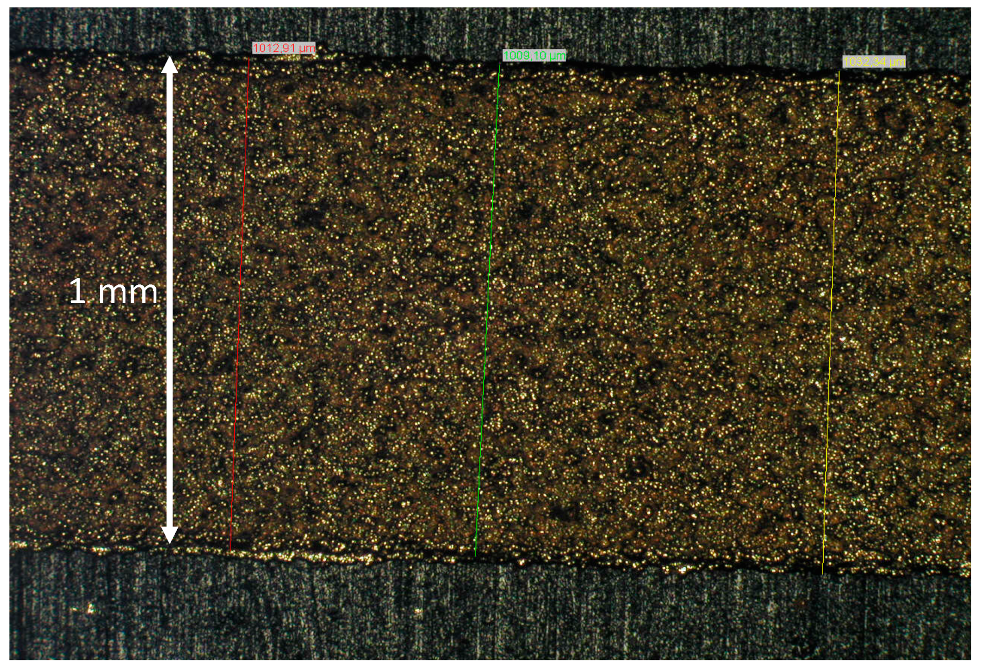
One important advantage of the LDS technique is that it makes it possible to obtain thick and robust metallization by chemical electroless deposition. The downside is the high degree of surface roughness, due to the action of the laser beam during activation [
16,
17]. Metal was deposited using commercial electroless solutions of copper, nickel, then gold. Deposition was examined with a stylus profilometer, showing surface roughness (Ra) equal to 5 μm and root mean square roughness (Rq) of 6.2 μm. To illustrate this roughness,
Figure 11 presents the profile of one of the microstrip lines of a filter under an optical microscope.
Measurements were made on the filters using a VNA E8364a (0–50 GHz) from Agilent
® and a universal test fixture 3680 V from Anritsu
®. The electrical responses of the two filters are shown in
Figure 9a and
Figure 10a, where the experimental data are compared with simulations. Despite differences observed between simulated and measured responses, the results validate the approach taken, as in each case an electrical response was obtained with all of the six poles in the bandwidth. Several differences can be observed in the experimental responses. First, there is a slight shift of the central frequency by about 1% that can be attributed to technological dispersions on the dimensions of the plastic piece, to the mechanical drillings, and at the first order to the uncertainty of the relative dielectric permittivity value of the thermoplastic. Second, the transmission levels in the attenuated bands are higher, due to the fact that parasitic couplings between the access microstrip lines of the filter are accentuated by the test fixture. It should be remembered that the filters are very short in length, less than 5 cm, thus promoting such couplings. Third, the matching levels are a few decibels higher than expected, hence impacting the level of insertion losses. This can be explained by the lower electrical conductivity of the LDS metallization, composed of copper but also of a thin layer of nickel/phosphorus, in comparison with a typical PCB copper layer. It also can be explained by the non-uniform roughness and the presence of some discrepancies in the dimensions: thickness of the microstrip access part, width of the microstrip lines, and positioning of the inductive posts.
In our measurement conditions, the insertion losses are higher for the 2.5% and 4.5% relative bandwidth filters by about 1 and 0.6 dB, respectively. However, we are able to extract, following [
14], a correct estimation of the quality factor of the fabricated filters. By considering 0.35 dB losses for each transition, we obtain a value of around 300 for both filters.
These results can be compared with the results of other solutions, extracted from the literature.
Table 4 summarizes the features of two relevant solutions realized at 35 and 83 GHz, based on the well-known RO5880, whose electrical characteristics are very close to the ones of the cyclo-olefin polymer. As shown in
Table 4, we obtain similar or better electrical performances with dimensions quite comparable. However, the access lines are very different. The RO5880 working at 35 GHz has a thick coplanar waveguide (CPW) access line with a strip width of around 1.6 mm. For the RO5880 working at 83 GHz, a coupling aperture interface structure is used as WR10-SIW transition. In our case, there is a thin microstrip access line with a strip width of around 900 μm. This configuration minimizes the losses and the parasitic effects when connecting the filter with bonding wires, making the integration of the COP filter easier in a global system. The care taken in the design of the transition will make it possible to really obtain benefit from the performances of the filter.
5. Conclusions
In conclusion, through the presentation of very acceptable experimental electrical responses, we have demonstrated that high quality factor filters can be fabricated on COP substrates through a cost efficient and robust process, combining molding, machining and laser direct structuring for metallization. To provide an adequate demonstration, we chose to work with high order narrow-band filters in the millimeter wave range. Under these conditions, we approach the limits in terms of sensitivity. Indeed, we cumulated the tolerances of all the steps of fabrication. However, even at millimetric frequencies, the discrepancy between simulations and measurements is slight, and can be significantly minimized by a better knowledge of the permittivity of the polymer. If necessary, tuning elements could be added on each cavity. The process applied here for a millimeter wave miniature circuit is obviously applicable for real 3D devices presenting higher reliefs, and in the centimetric frequency range where the devices are larger and where the frequency shift would be negligible.
Compared to standard ceramic substrates, which are not easy to machine, COP offer the possibility of building 3-dimensional shapes that can satisfy both electrical constraints and interconnection compatibility with the other components in a complex system. In terms of loss tangent, COP are comparable to ceramics usually used in RF. Since the size is not a problem in high frequency, its low permittivity is an advantage for limiting the sensitivity of fabrication tolerance. Moreover, it is a low-cost material, well suited for mass production, and is thus perfectly suited to the chosen fabrication processes.
In terms of genericity we have designed a specific transition usable with different filters. We have also shown that a mold can be used for several different filters, which is another advantage with regard to cost considerations. Fabrication could be improved by choosing other metallization processes, such as inkjet, which would allow the use of COP not compatible with LDS, hence offering better characteristics in terms of loss tangent.
As the cost is one of the advantages of the fabrication process associated with this material, possible applications could be found in several domains where large series are needed: Radio front ends for Internet of Things, payload of satellite constellations, etc.

 ,
, 


