1. Introduction
The application of Poly(3,4-ethylenedioxy thiophene):polystyrenesulfonate (PEDOT:PSS) for photovoltaic applications has been a growing area of interest in recent years due to the opportunity for simple low-temperature processing and its anti-reflective properties [
1,
2,
3,
4,
5]. PEDOT:PSS is perhaps the most popular electronically active complex of the polythiophene family. In this form, the PSS acts as a p-type doping counter ion which allows hole mobility along the PEDOT conjugated backbone and promotes the dispersion of the complex in polar solvents such as water due to the micelle-like morphology that the complex develops. PEDOT:PSS has been studied previously for a variety of applications, but its behavior in solid state electronic devices, such as diodes and transistors, is not yet completely understood. For understanding the behavior of PEDOT:PSS to be like that of a p-doped semiconductor, different photovoltaic device architectures have been studied with emphasis on all-organic devices. Nevertheless, due to its compatibility with traditional semiconductors, hybrid organic-inorganic devices have been developed that have shown better performance than the all-organic counterparts. One of the most promising of such hybrid devices uses PEDOT:PSS on n-type silicon as a front emitter. This cell structure has reached a maximum PCE of 14.6% on planar silicon substrates [
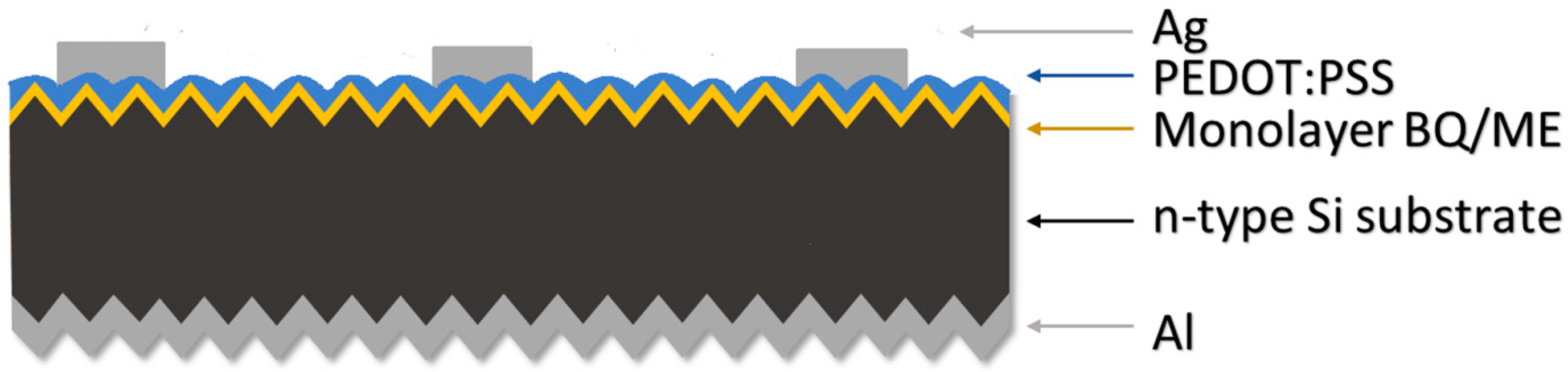
1]. The general structure of this hybrid solar cell can be seen in
Figure 1. In this structure, the PEDOT:PSS layer acts as a hole carrier selective contact which induces a photoactive junction with the n-type silicon and acts as an anti-reflective coating. This architecture also often involves a passivation treatment of the silicon surface previous to the PEDOT:PSS deposition which contributes to minimizing the surface defect density, minimizing the charge recombination, and the improving open circuit voltages.
One of the main advantages of using PEDOT:PSS, besides its relatively low-cost and simple processing, is its potential to increase the photo collection efficiency of photovoltaic devices by acting as an anti-reflective coating. Texturing the active substrate is another common method used to improve the photo collection. In this work, we aim to take advantage of both of these techniques by using textured silicon substrates as our base in order to maximize the photo collection of the device. Achieving this effect, however, poses several unique design challenges. Just like any other anti-reflective treatment, the anti-reflective properties of PEDOT:PSS are optimized at a specific film thickness. Furthermore, the homogeneity of the film is crucial not only for the anti-reflective effect but also for proper device performance, as incomplete or otherwise faulty coatings will cause shunts that will drastically hinder the efficiency of the device.
Therefore, for the fabrication of efficient hybrid devices, it is critical to accurately control the deposition procedure to achieve homogeneity and a proper thickness of the film. Spin coating has been the preferred casting method for PEDOT:PSS as it allows for very thin homogeneous films to be produced. In spin coating, the rheological properties of the fluid being cast, its interfacial interaction with the substrate, as well as the spin speed and time, ultimately determine the thickness and homogeneity of the resulting film. Spin coating parameters tend to produce highly reproducible results; however, this has only been validated for planar smooth substrates. Irregular or textured substrates, such as those used in this study, have not been studied as thoroughly in the context of spin coating thus additional rigor is required to validate the spin coating procedure in order to confirm the homogeneity and coverage of the films.
Carrier collection is another major concern in designing solar cells. For our devices, we employ a silver fingers-bus bar scheme as a front contact deposited by electron beam physical vapor deposition with the use of a shadow mask. In designing the shadow mask for the contact, the primary goal is to minimize the shading caused by the metal while maintaining an optimal carrier collection. The efficiency of carrier collection is limited by transport losses through each of the materials and at the interfaces between them. For ohmic contacts, the transport losses at the interface are inversely proportional to the total contact area, such that there is a tradeoff between losses due to shading and those due to transport. In order to design the shadow mask, losses due to the metal contact resistance and shading, the contact resistance at the interface, and the resistance of the PEDOT:PSS must be quantitatively determined and optimized. This optimization was performed using the open access PV Lighthouse calculator [
6]. In this case, silver was used as the front metal contact due to its high bulk conductivity and its reported compatibility with PEDOT:PSS, the specifics of which have not been adequately investigated previously. In this work, we quantitatively characterize the electrical properties of the Ag/PEDOT:PSS interface and used these results for our mask design. We demonstrate this interface develops ohmic characteristics with an even lower resistance than previously reported.
It is not surprising that the performance of these hybrid solar cells is highly dependent on the properties of the PEDOT:PSS film, particularly its optical and electrical properties, and the behavior of the interfaces between the materials. PEDOT:PSS behaves like a degenerate p-type semiconductor which is why it induces a photoactive junction with n-type silicon, with the depletion region located exclusively in the active silicon layer. By using geometric considerations, the doping concentration of PEDOT:PSS can be estimated to be 3 × 10
20 cm
−3 [
7] (p. 147). Due to the chemical nature of the PEDOT:PSS complex this number is unlikely to vary significantly and thus its contribution to the junction is predictable and reproducible. Despite having such a high carrier concentration, the conductivity of PEDOT:PSS is limited by the carrier mobility and results in a much lower conductivity than traditional metals and semiconductors, which has prompted numerous studies on improving it by different methods [
3,
4,
5]. One such method is the addition of co-solvents to the PEDOT:PSS dispersion which modifies its structural morphology, promoting the closer packing of the micelle which in turn results in better conductivity of the deposited films [
4]. Solutions of ethylene glycol (EG) and dimethyl sulfoxide (DMSO) have emerged as the most effective co-solvents for this purpose [
8].
In this work, we aim to understand the implications of using the two co-solvents mentioned previously, EG and DMSO, in the design and fabrication of hybrid solar cells which employ a benzoquinone solution-based surface passivation treatment, a pyramidal textured silicon active layer, and a silver bus bar-finger front metal contact [
9]. First, we validate the spin coating procedure for the PEDOT:PSS dispersions on textured substrates by analyzing the homogeneity and uniformity of the films. Second, we test the effects of these co-solvents on the electrical properties of PEDOT:PSS films. Third, we characterize the effects of the co-solvents on the photo collection efficiency of our device architecture. Fourth, we quantitatively characterize the electrical interfacial behavior between PEDOT:PSS and silver. Finally, we fabricate and characterize the hybrid solar cells, following the design described previously, using these co-solvents, and explore their effects on device performance.
2. Materials and Methods
N-type silicon (100) textured substrates (doped with phosphorous, CZ) with a back surface field (BSF) were fabricated at Arizona State University (Solar power lab, ASU, Tempe, AZ, USA). These wafers are 145 microns thick with 1–5 ohm-cm resistivity. Random texturization was performed on both sides using potassium hydroxide (2% KOH yielding pyramid sizes of about a 3–5 µm base size) alkaline etching. To create BSF n+ layer on the N-type wafers, phosphorous oxychloride diffusion was performed at 820 °C for 15 min with a POCl3 carrier gas flow rate of 1500 sccm (standard cubic centimeters per min). This step is for the phosphosilicate glass (PSG) growth and drive-in. Finally, the wafers were then exposed to a 10 min buffered oxide etch to remove the PSG. The sheet resistance value of the BSF side is 55 ohm/square. Double-side polished intrinsic silicon substrates were purchased from Virginia Semiconductors (Fredericksburg, Virginia, USA). These polished wafers are 300 microns thick and have a resistivity >5000 ohm-cm.
PEDOT:PSS PH1000 (Heraeus Clevios, Vandalia, OH, USA) was used as the stock polymer dispersion. The solvents ethylene glycol (EG), dimethyl sulfoxide (DMSO), and surfactant Triton X-100 (non-ionic surfactant) were purchased from Fischer Chemical (Waltham, MA, USA) (>95%) and used as purchased.
All wafers were cleaned following the procedures described by Opila and Teplyakov et al.: the substrates were cleaned using a Piranha etch (H
2SO
4:H
2O
2 = 4:1) for 5 min, followed by a 5-min DI water rise and a 2-min immersion in hydrofluoric acid (HF, 2 wt%) [
10]. After cleaning, the substrates were quickly dried by blowing nitrogen and immediately placed in the passivation solution of benzoquinone (BQ) and methanol (MeOH) [
9]. The wafers are allowed to stay in the sealed bag containing a passivation solution for 2 h in ambient light conditions. Passivation studies performed in the group previously have suggested that benzoquinone (BQ) does an effective job of passivating the surface. PEDOT:PSS does not possess notably good passivation properties and, hence, the role played by the BQ in these cells is critical. Post-2-hour immersion in BQ, the wafers were removed and given a quick rinse with methanol. The wafers were dried and put on a spinner chuck for spin coating.
PEDOT:PSS dispersions were prepared in advance of the spin coating procedure by adding the appropriate co-solvent amounts as well as 0.25 wt% Triton X-100 as a surfactant. The dispersions were then deposited by spin coating on the appropriate wafers at different spin conditions in a Headway Research (Garland, TX, USA) spin coater. All spin-coated samples were baked on a hot plate at 135 °C for 15 min immediately following the PEDOT:PSS deposition.
Textured silicon wafers of 1 cm × 1 cm were used as substrates for the validation study of the spin coating procedure. An X-ray energy dispersive spectroscopy (XEDS) analysis was conducted on a JEOL JSM-7400F (Peabody, MA, USA) scanning electron microscope (SEM). X-ray photoelectron spectroscopy (XPS) measurements were conducted on a Physical Electronics (PHI) model 5600 X-ray photoelectron spectrometer (Chanhassen, MN, USA) using an Al 7 mm filament monochromated source with an X-ray energy of 1486.6 eV.
Double-side polished intrinsic silicon wafers were used as substrates for the PEDOT:PSS conductivity measurements. Conductivity measurements were carried out by the van der Pauw technique on a custom built room temperature resistivity and Hall Effect system [
11]. The resistivity of the films was measured twice (bi-directional by switching the four contacts between voltage and current probes) and the resulting values were averaged.
Device reflectivity measurements were carried out on 2 cm × 2 cm textured silicon substrates with different PEDOT:PSS spin-coated recipes. A Perkin-Elmer Lambda 750 UV/Vis/NIR spectrophotometer (Hopkinton, MA, USA) was used to conduct ultraviolet-visible spectrophotometry (UV-VIS).
Textured silicon wafers of 1 cm × 1 cm were used as substrates for the transmission line measurements (TLM). Ag contact pads that are 500 nm thick were deposited via electron beam physical vapor deposition with length L = 0.5 mm and width W = 10 mm at spacings of d = 0.1 mm, 0.2 mm, 0.4 mm, 0.8 mm, 1.6 mm, and 3.2 mm. The resistance was measured between adjacent sets of contact pads with a Keithley 2400 sourcemeter (Beaverton, OR, USA).
Completed 1 cm × 1 cm solar cell devices were fabricated on textured silicon wafers prepared using the described cleaning procedure. After approximately 10 min, appropriate PEDOT:PSS dispersions were then spin-coated on the front of the wafers (face without BSF) through a 0.22-micron filter. Metal contacts were then deposited on the samples via electron beam physical vapor deposition on a dual electron-beam evaporator (Wilmington, MA, USA). Aluminum was used as the back contact and deposited on the BSF-treated side of the wafer, while silver was used as the front contact and was deposited with the help of a shadow mask directly on the PEDOT:PSS films. The shadow mask which was designed following the guidelines described previously had a total power loss of 19%, 10.4% due to shading, 6% estimated due to contact resistance, and the remaining estimated due to resistive losses in the PEDOT film and Ag fingers.
The performance of these devices was evaluated using illuminated current density-voltage measurements (JV). The JV response was measured by means of a DC source meter (Keithley 2400 sourcemeter (Beaverton, OR, USA)) both in dark and light, under an air mass 1.5 G standard illumination.
3. Results
3.1. PEDOT:PSS Coating Uniformity on Textured Substrates
Due to the texturing of the substrate and the addition of co-solvents, the quality of the spin-coated PEDOT:PSS films had to be validated in order to confirm proper homogeneity and uniformity. Furthermore, the performance of an anti-reflective coating is dependent on the thickness of the film and the wavelength of light such that there is an optimal thickness for the solar spectrum that optimizes photo-collection and device performance. In the case of PEDOT:PSS, previous simulations performed using the online optical simulator OPAL 2 suggested an optimal thickness of 65 nm on a planar silicon substrate for the optimization of the anti-reflective properties of the coating at AM1.5g direct illumination conditions [
12,
13]. Previous ellipsometry studies on PEDOT:PSS with both EG and DMSO spin-coated on planar silicon substrates have confirmed the reproducible film thickness results for different spin conditions: 4000 rpm for 300 s having a thickness of 50 nm and 2250 rpm for 300 s for a thickness of 65 nm [
12].
Testing the thickness of PEDOT:PSS films spin-coated on textured surfaces poses a technical challenge as it is obvious that the texturing of the substrate induces additional roughness and inhomogeneity to the films. In fact, preliminary ellipsometry studies of films deposited on textured substrates confirm significant thickness variations throughout the deposition area, such that we are not confident in reporting the thickness of these films quantitatively. Due to the additional roughness and inhomogeneity introduced, it was important to confirm the complete coverage of the substrates as it is not immediately obvious that the spin coating procedure on these substrates guarantees complete coverage. It is also important to, at least qualitatively, understand the magnitude of the thickness variation of the film throughout the deposition area.
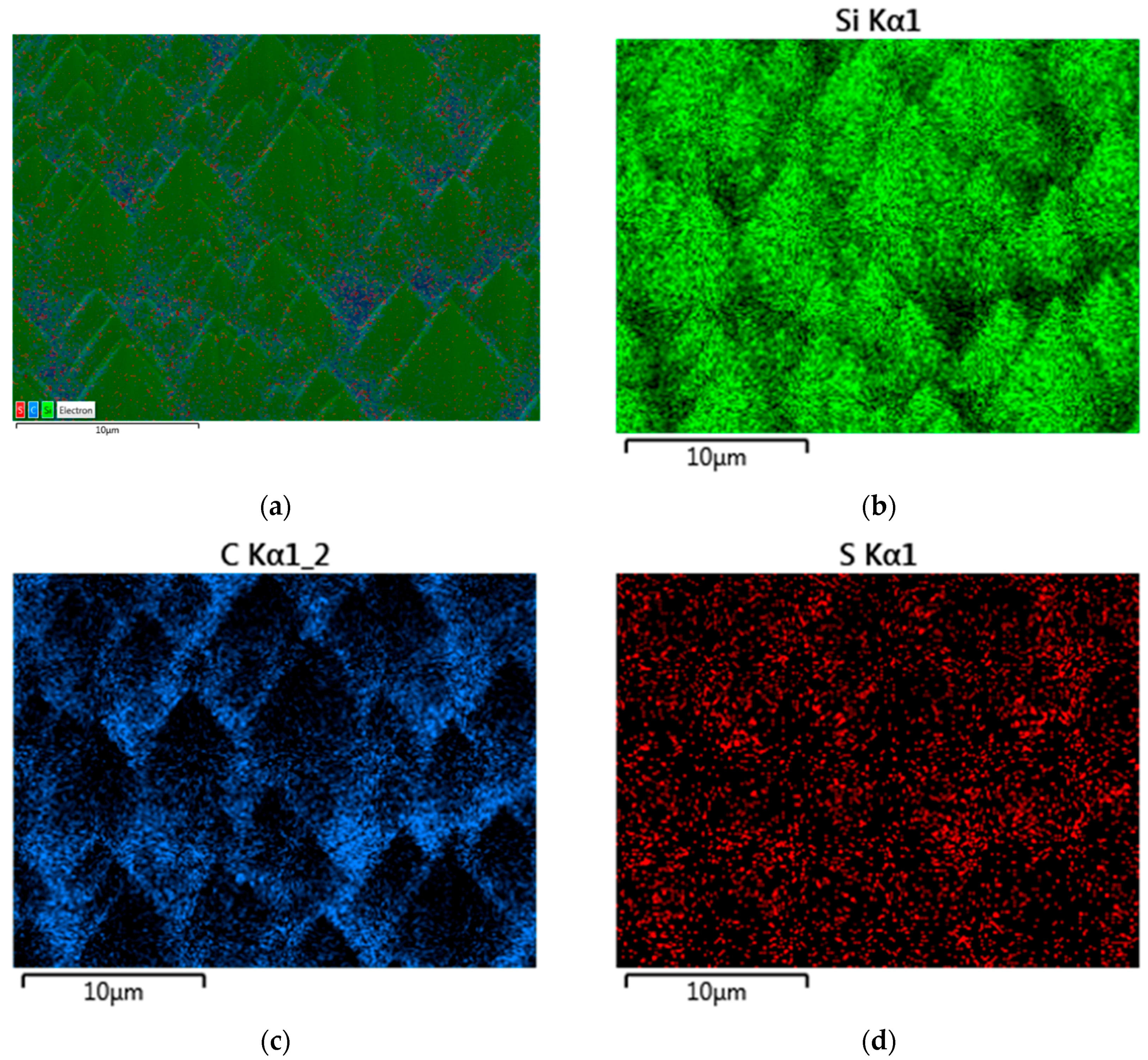
PEDOT:PSS dispersions containing 7 wt% EG or DMSO were spin-coated on textured silicon wafers at 2250 rpm for 300 s. X-ray Energy Dispersive Spectroscopy (XEDS) and X-ray Photoelectron Spectroscopy (XPS) were conducted on the samples in order to confirm the complete coverage of the substrates and study the homogeneity of the films.
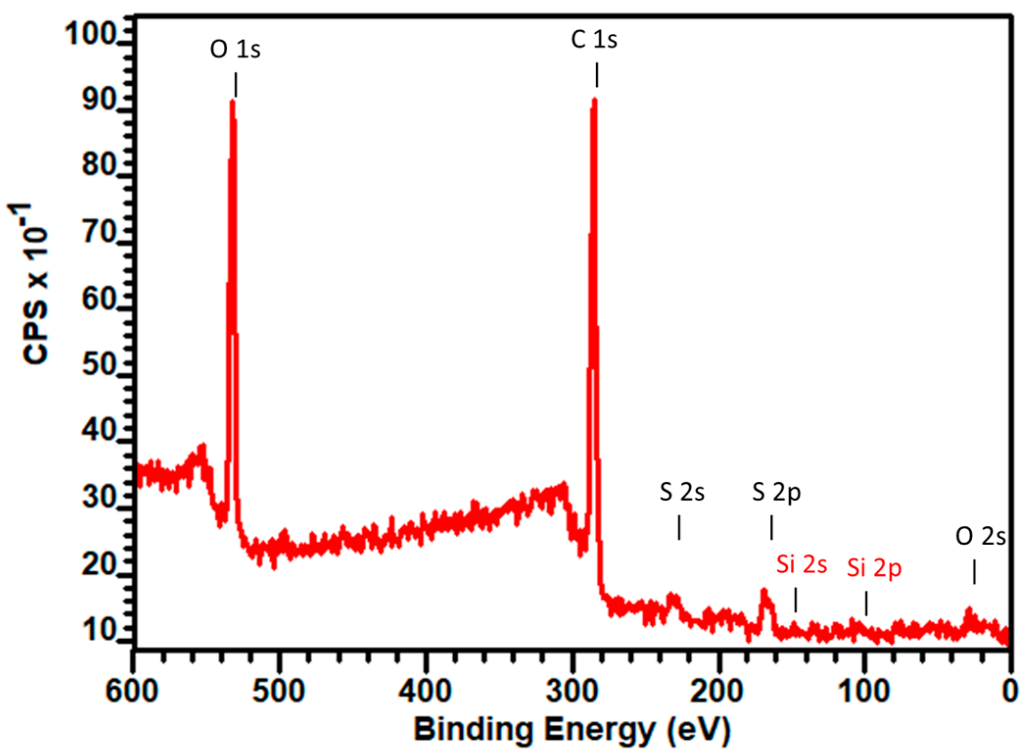
Figure 2 shows the elemental mapping results of the XEDS analysis. The image reveals a greater concentration of C and S near the base of the pyramids of the substrate, indicating that during the spin coating, the PEDOT:PSS accumulates in the valleys of the texturing. It is difficult to establish complete PEDOT:PSS coverage of the silicon substrate based on the XEDS data alone due to the probing depth of the electron beam being thicker than the PEDOT:PSS films. XPS is a more surface sensitive technique and is capable of probing the first few nanometers of the sample. XPS analysis (
Figure 3) revealed that no significant concentration of silicon was present at the surface of the samples, confirming complete coverage of PEDOT:PSS and indicating a lack of significant shunt through-holes in the PEDOT:PSS layer. Based on these results we can say that the reliability of the spin coating procedure translates well to the textured substrates and the use of co-solvents, but the accumulation phenomenon towards the valleys of the texturing is pervasive and its implications must be considered carefully. This accumulation phenomenon occurred in all the samples tested, however, from these techniques alone it is not possible to quantitatively characterize the irregularity of the film.
3.2. Effect of Co-Solvents on the Electrical Properties of the PEDOT:PSS Films
PEDOT:PSS dispersions with different co-solvent compositions were spin-coated on planar silicon substrates, as opposed to the textured substrates used for devices, at different spin conditions and their electrical properties were tested by the van der Pauw technique. The additional roughness introduced by the substrate texturing would cause a large error that would make the results not comparable among themselves.
Table 1 shows the electrical properties of the various films tested.
It is no surprise that lower spin speeds and correspondingly thicker films, produce films with lower sheet resistance. Although these results are not directly translatable to the films spin-coated on textured substrates, as these films are considerably less homogeneous, we confirm the significant enhancement of conductivity by using co-solvents. Furthermore, we can confirm that at the target thickness, for anti-reflective optimization, of 65 nm (2250 rpm), 7 wt% EG produces the lowest sheet resistance of all samples tested. Therefore at this spin condition, the anti-reflective properties of PEDOT:PSS and the sheet resistance of the film are optimized for a planar substrate; thicker films will have lower sheet resistance but will compromise the anti-reflective properties. However, as will be discussed in more detail in later sections, optimizing the anti-reflective properties, which are directly related to the thickness of the films, and the conductivity of films deposited on textured substrates is not as straightforward and requires a more empirical approach. It is also important to note that for irregular films the effective sheet resistance of the film will be limited by the thinner regions of the film. In other words, if the dispersion is more prone to accumulation in the valleys of the texturing then the thinner regions in the peaks of the pyramids will limit the overall conductivity of the film.
Previous work has explored the mechanisms by which co-solvents affect the conductivity of PEDOT:PSS dispersions. In this case, the co-solvents modify the micelle-like morphology of the PEDOT:PSS complex, in which the flexible PSS molecules encapsulate the rigid PEDOT chains forming a voluminous shell (this structure is commonly referred to as a gel) [
7] (p. 115). In this structure, the doped conjugated PEDOT backbone is the only pathway for charge transport, as PSS is not electronically active and only contributes to doping the PEDOT and inducing its solubility. The addition of co-solvents decreases the thickness of the PSS shell and induces a rearrangement of the PEDOT chains, from the coil-like benzoid structure that may be present along the grain boundaries to a more linear or extended quinoid structure resembling stacked pancakes [
4,
7,
8,
14,
15]. Combined, these structural modifications promote the closer packing of the PEDOT chains which in turn facilitates cross-chain charge transfer [
4]. This, in turn, results in a higher bulk conductivity and lower sheet resistance.
3.3. Effect of Co-Solvents on the Anti-Reflective Properties of Devices
Although quantitatively characterizing the thickness and irregularity of the PEDOT:PSS films on textured substrates is challenging, measuring the anti-reflective properties of the devices allows us to directly assess the impact of the spin conditions on the photo collection efficiency of the device and empirically deduce the resulting irregularity of the films.
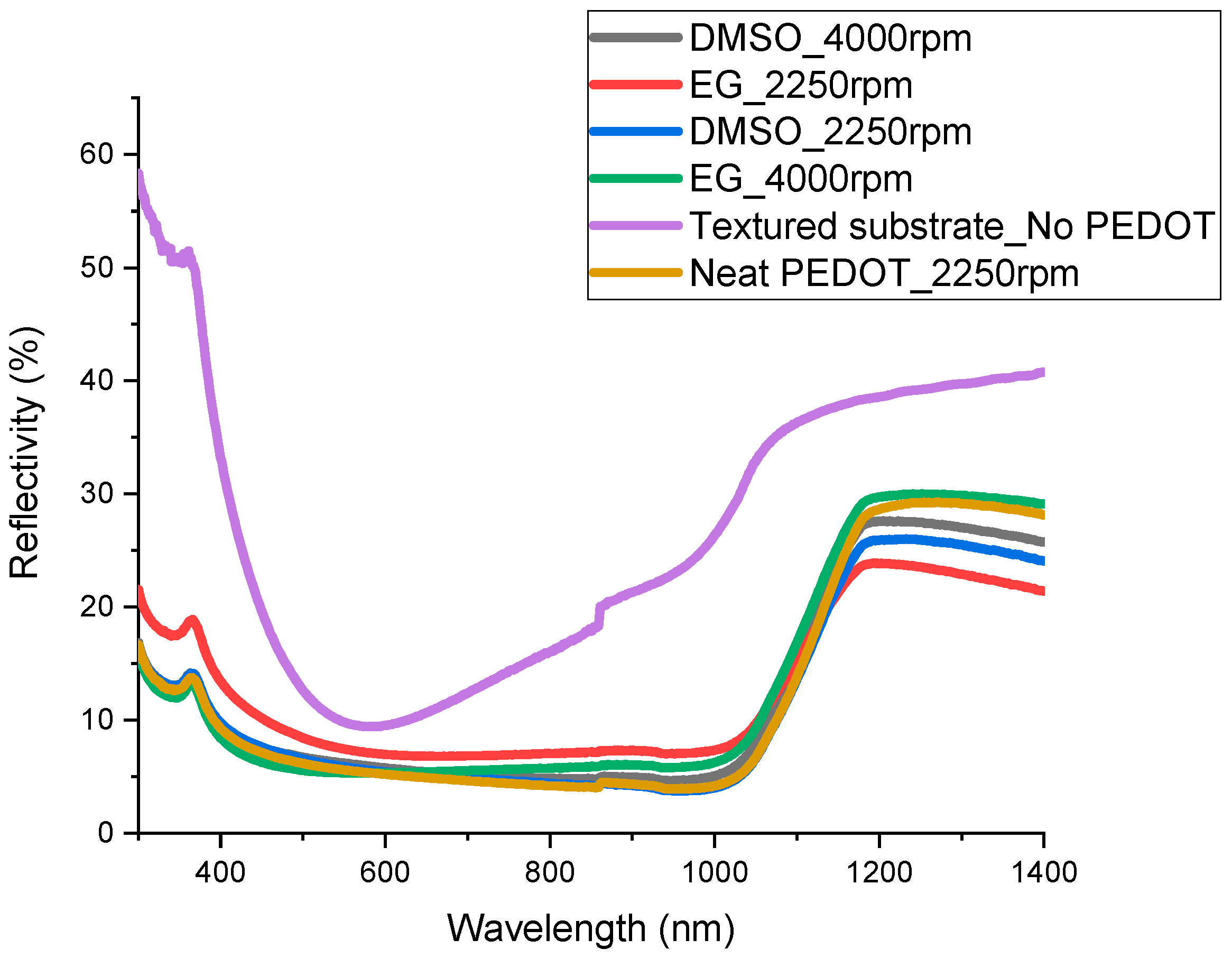
Figure 4 shows the UV-VIS reflection spectrum collected for the PEDOT:PSS films spin-coated on textured silicon wafers with different co-solvent compositions. It can be readily seen that the PEDOT:PSS films significantly reduce the reflectivity of the devices, confirming its anti-reflective properties. We can also observe that the addition of co-solvents does not affect the anti-reflective properties of the resulting films significantly. PEDOT:PSS has a transmission of more than 90% throughout the solar spectrum.
Nevertheless, there are some slight differences between spin recipes that are important to point out. Particularly, PEDOT:PSS with 7 wt% EG has a better anti-reflective performance in the visible spectrum when spin-coated at 4000 rpm than 2250 rpm. DMSO, on the other hand, seems to perform just as well at either spin speed. The difference in anti-reflective performance seen for EG may be due to the rheological properties of the dispersion and their implications in spin-coating on a textured substrate. Although it is difficult to confirm the specific impacts of the rheological properties on the thickness distribution of the films obtained in these cases, the anti-reflective performance suggests that, at least for EG, 4000 rpm produces films with a thickness closer to 50 nm throughout the silicon substrate [
12]. In other words, dispersions with EG are more sensitive to pooling which can be overcome by spinning at higher speeds. DMSO, on the other hand, produces films which are more resistant to pooling and thus are more homogeneous. The implications of the difference in homogeneity of the films coated on textured substrates are important to consider in order to optimize their electrical performance. The more inhomogeneous films produced with EG at 2250 rpm will not only have a lower anti-reflective performance but may also have higher sheet resistance, as this property is limited by the thinnest regions of the film.
3.4. Characterization of the Ag/PEDOT:PSS Interface
As mentioned earlier, the contact resistivity between Ag and PEDOT:PSS is a critical parameter in designing the front contact and it is not well understood or reported. In the case of the devices presented in this work, the major limiting loss factor was initially assumed to be the resistance of the Ag/PEDOT:PSS interface. Mahato et al. performed a contact resistivity measurement for Ag thermally deposited on PEDOT:PSS films (Clevious PH 1000, with a 5 wt% DMSO cosolvent and 0.1% Capstone FS-31 fluoro-surfactant) on planar glass substrates and found contact resistivities of 0.79 Ohm·cm
2 [
10]. Such large contact resistivities would make this interfacial resistance the largest source of power loss in the design of a front contact shadow mask. Furthermore, measurements from initial devices indicated that the total series resistance, as measured from the JV slope plateau beyond Voc, can reach down to 1 Ohm·cm
2. By analyzing the specific contact grid design in the PV Lighthouse Grid calculator, an upper bound of 0.064 Ohm·cm
2 can be deduced for the Ag contact resistivity in such devices. Clearly, the existing literature value for Ag contact resistivity was not applicable to the performance observed for most PEDOT:PSS devices on Si substrates. We used the transmission line measurement (TLM) to quantitatively characterize the electrical properties of this interface for the PEDOT:PSS films with co-solvents and use these results directly in our device design.
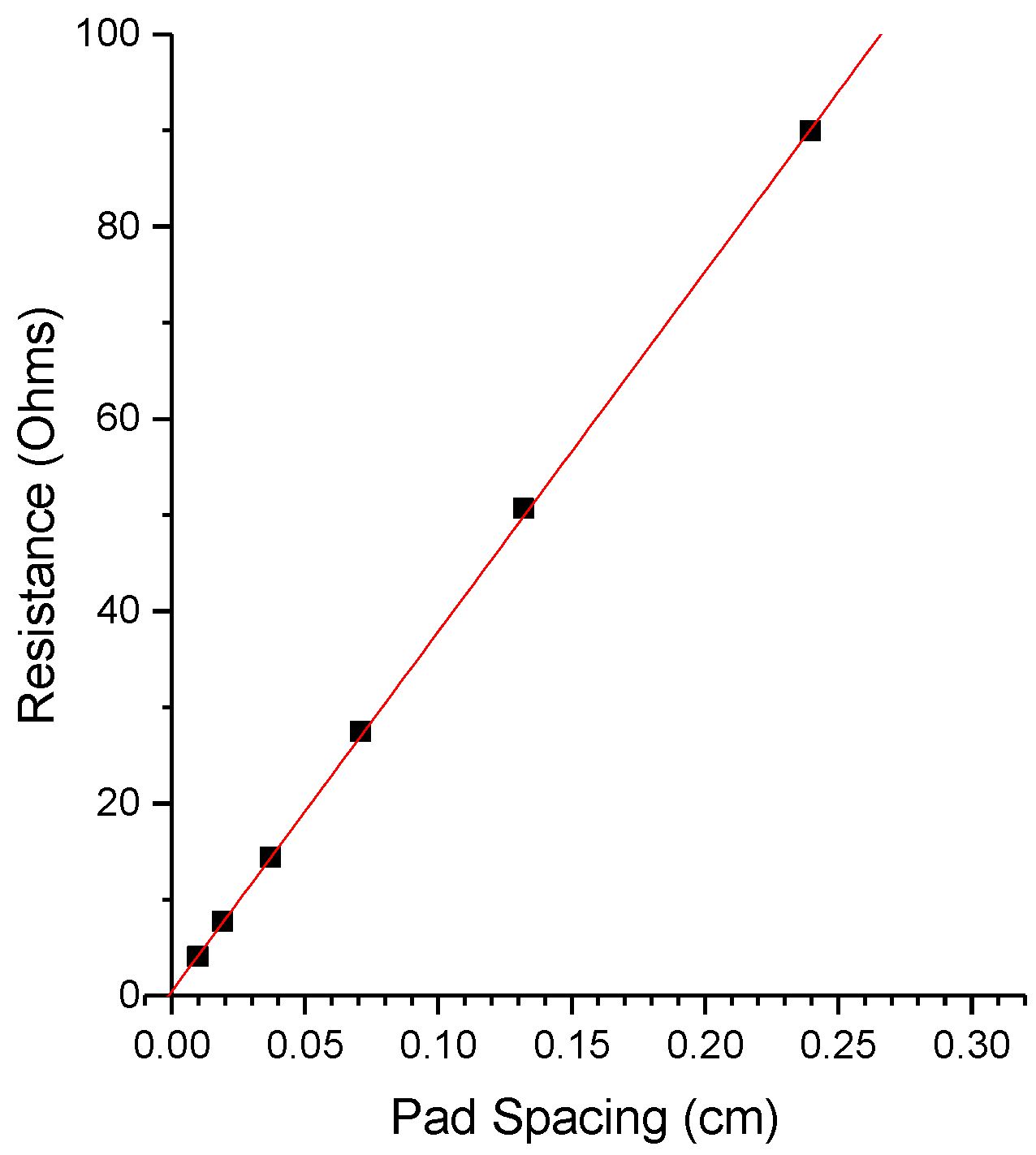
Figure 5 shows the results obtained from the TLM measurements of PEDOT:PSS films with different co-solvents spin-coated on textured silicon substrates.
Table 2 shows the results obtained from the TLM data by the general analytical approach described by Schroder, including a correction factor to account for the edge effects of the contact pads [
16]. Any nonlinearities in the fit can propagate into large errors in the estimation of the x- and y-intercepts used to calculate the contact resistance and transfer length. Here the effect of fitting errors was minimized by forcing the fit slope to pass through the first measured resistance data point. Using this approach, a low contact resistivity of 0.000133 Ohm·cm
2 was found. The range of the possible values using the 95% confidence interval for the slope and y-intercept are also reported in
Table 2. The contact resistivity obtained for this specific device design is drastically lower than the previously reported values, indicating that Ag/PEDOT:PSS contact resistivity is not the series resistance bottleneck and can be largely neglected in future shadow mask design. These results indicate much lower shading ratios than can be achieved with the 10.4% mask used in this paper. Future devices could utilize masks with 4.8% shading ratios where front grid power losses are limited primarily by the sheet resistance of the PEDOT:PSS layer itself. The extent to which the choice of co-solvents modifies the contact resistivity for this interface has yet to be studied.
In addition to measuring contact resistivity, TLM can provide a reliable measurement of sheet resistance, since errors in the fit slope are typically small. For the case of a film with 7% DMSO spin-coated at 4000 rpm for 300 s, the measured sheet resistance was 374 Ohm/. This sheet resistance measurement is in good agreement with the 296 Ohm/ measured via the van der Pauw technique. The TLM measurements were performed on textured partially conductive (1–5 Ohm-cm) samples, which give a sheet resistance more relevant to the actual device conditions, but do not allow for the full isolation of the PEDOT:PSS conductivity. Additional variations can be expected as the Van der Pauw method measures the sheet resistance of the full sample, including any edge irregularities in spin-coating thickness, while the TLM method is more isolated to the central region of the sample.
3.5. Hybrid Solar Cell Fabrication and Characterization
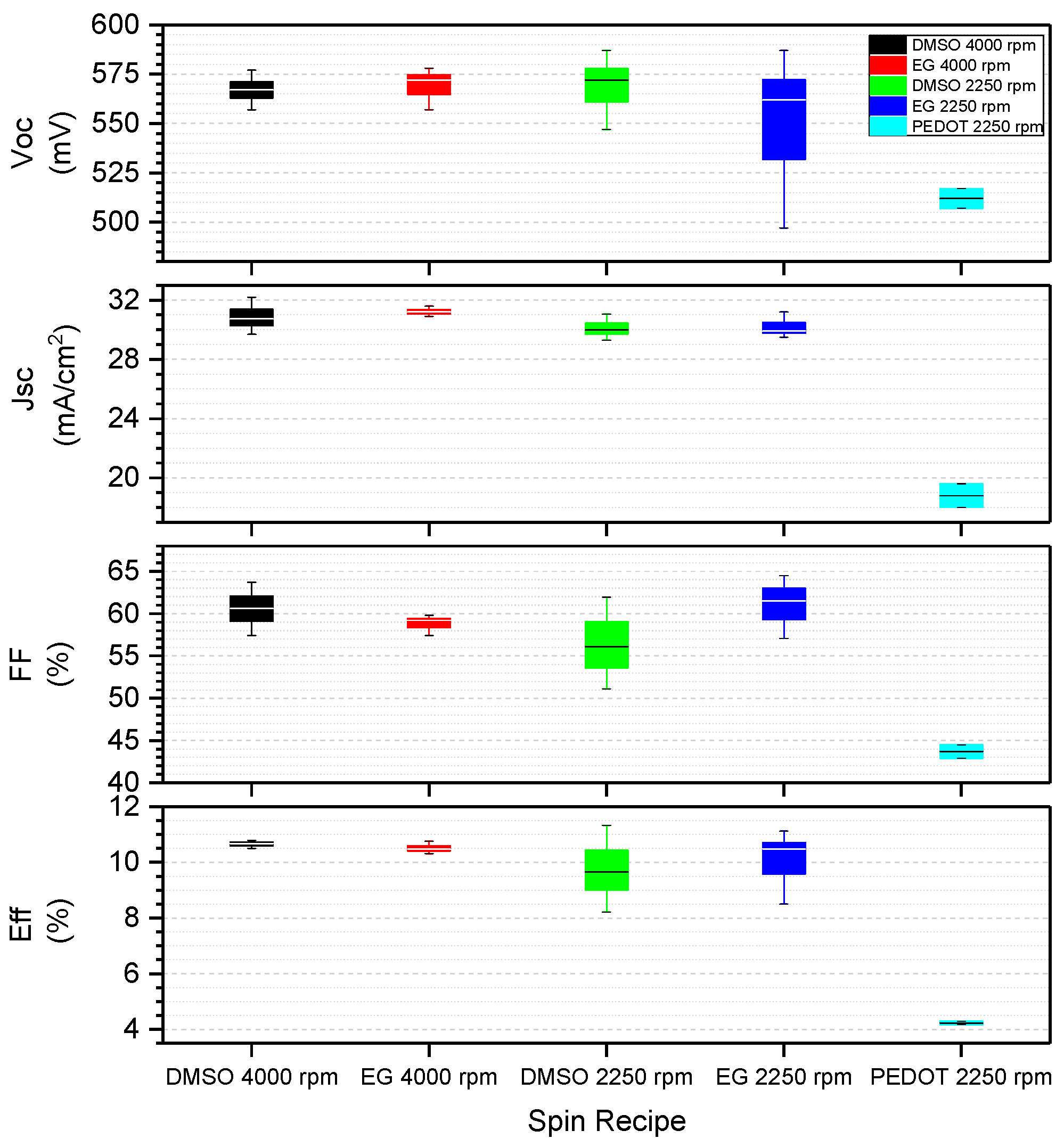
Table 3 shows the performance of the solar cells, as measured by illuminated JV, fabricated with different PEDOT:PSS recipes. The devices were fabricated using the process described in
Section 2. Multiple devices were fabricated for each recipe, in order to understand the variations in device performances.

 ,
, 


