Quantum Dot Solar Cells: Small Beginnings Have Large Impacts


Abstract
Featured Application
Abstract
1. Introduction
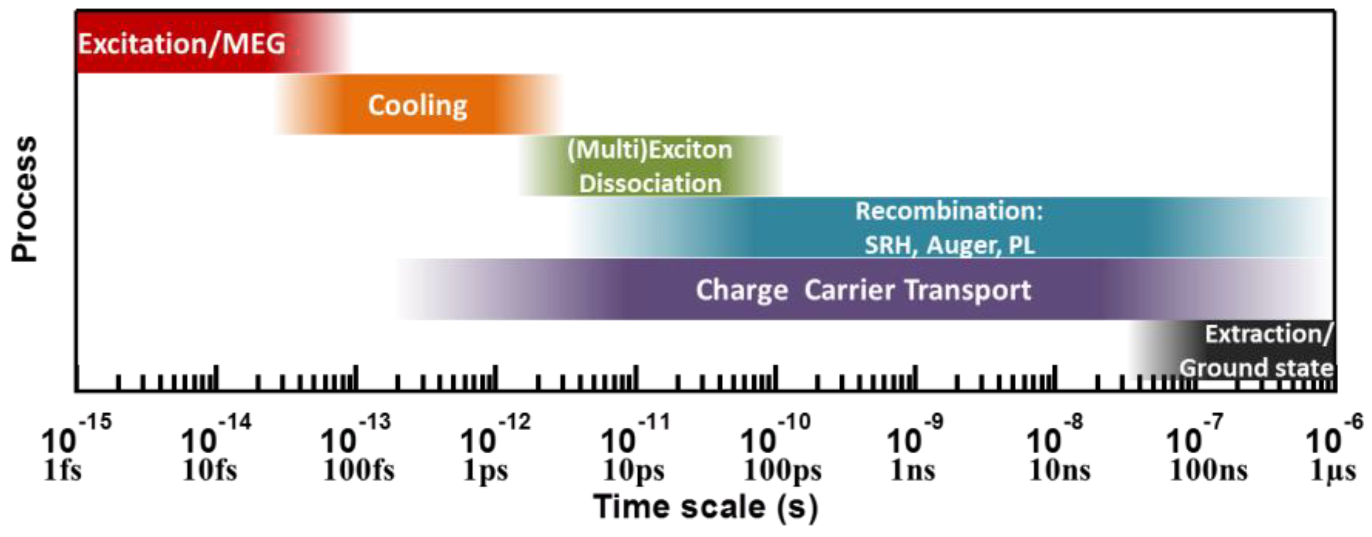
2. Timescales of Excited State Processes
2.1. Absorption and Multiple Exciton Generation
2.2. Cooling
2.3. Charge Carrier Transport
2.4. (Multi)Exciton Dissociation
2.5. Recombination
2.6. Extraction
3. Quantum Dot Solar Cells
Supplementary Materials
Author Contributions
Funding
Acknowledgments
Conflicts of Interest
References
- Brus, L. Electronic wave functions in semiconductor clusters: Experiment and theory. J. Phys. Chem. 1986, 90, 2555–2560. [Google Scholar] [CrossRef]
- Efros, A.L.; Rosen, M. Quantum size level structure of narrow-gap semiconductor nanocrystals: Effect of band coupling. Phys. Rev. B 1998, 58, 7120–7135. [Google Scholar] [CrossRef]
- Aabhash, S.; Munkhbayar, B.; Antonio, T.; Sheng, D.; Zhang, Q.S. Recent advance in near-infrared active lead chalcogenide quantum dots: Preparation, post-synthesis ligand exchange and applications in solar cells. Angew. Chem. Int. Ed. 2018. [Google Scholar] [CrossRef]
- Lim, J.; Bae, W.K.; Kwak, J.; Lee, S.; Lee, C.; Char, K. Perspective on synthesis, device structures, and printing processes for quantum dot displays. Opt. Mater. Express 2012, 2, 594–628. [Google Scholar] [CrossRef]
- Murray, C.B.; Kagan, C.R.; Bawendi, M.G. Synthesis and characterization of monodisperse nanocrystals and close-packed nanocrystal assemblies. Annu. Rev. Mater. Sci. 2000, 30, 545–610. [Google Scholar] [CrossRef]
- Kershaw, S.V.; Susha, A.S.; Rogach, A.L. Narrow bandgap colloidal metal chalcogenide quantum dots: Synthetic methods, heterostructures, assemblies, electronic and infrared optical properties. Chem. Soc. Rev. 2013, 42, 3033–3087. [Google Scholar] [CrossRef] [PubMed]
- Owen, J.; Brus, L. Chemical synthesis and luminescence applications of colloidal semiconductor quantum dots. J. Am. Chem. Soc. 2017, 139, 10939–10943. [Google Scholar] [CrossRef] [PubMed]
- van Embden, J.; Chesman, A.S.R.; Jasieniak, J.J. The heat-up synthesis of colloidal nanocrystals. Chem. Mater. 2015, 27, 2246–2285. [Google Scholar] [CrossRef]
- Goubet, N.; Jagtap, A.; Livache, C.; Martinez, B.; Portalès, H.; Xu, X.Z.; Lobo, R.P.S.M.; Dubertret, B.; Lhuillier, E. Terahertz hgte nanocrystals: Beyond confinement. J. Am. Chem. Soc. 2018, 140, 5033–5036. [Google Scholar] [CrossRef] [PubMed]
- LaMer, V.K.; Dinegar, R.H. Theory, production and mechanism of formation of monodispersed hydrosols. J. Am. Chem. Soc. 1950, 72, 4847–4854. [Google Scholar] [CrossRef]
- Sugimoto, T.; Shiba, F.; Sekiguchi, T.; Itoh, H. Spontaneous nucleation of monodisperse silver halide particles from homogeneous gelatin solution i: Silver chloride. Colloids Surf. A Physicochem. Eng. Asp. 2000, 164, 183–203. [Google Scholar] [CrossRef]
- Liu, H.; Owen, J.S.; Alivisatos, A.P. Mechanistic study of precursor evolution in colloidal group II–VI semiconductor nanocrystal synthesis. J. Am. Chem. Soc. 2007, 129, 305–312. [Google Scholar] [CrossRef] [PubMed]
- Clark, M.D.; Kumar, S.K.; Owen, J.S.; Chan, E.M. Focusing nanocrystal size distributions via production control. Nano Lett. 2011, 11, 1976–1980. [Google Scholar] [CrossRef] [PubMed]
- Hendricks, M.P.; Campos, M.P.; Cleveland, G.T.; Jen-La Plante, I.; Owen, J.S. A tunable library of substituted thiourea precursors to metal sulfide nanocrystals. Science 2015, 348, 1226–1230. [Google Scholar] [CrossRef] [PubMed]
- Campos, M.P.; Hendricks, M.P.; Beecher, A.N.; Walravens, W.; Swain, R.A.; Cleveland, G.T.; Hens, Z.; Sfeir, M.Y.; Owen, J.S. A library of selenourea precursors to PbSe nanocrystals with size distributions near the homogeneous limit. J. Am. Chem. Soc. 2017, 139, 2296–2305. [Google Scholar] [CrossRef] [PubMed]
- Hamachi, L.S.; Jen-La Plante, I.; Coryell, A.C.; De Roo, J.; Owen, J.S. Kinetic control over CdS nanocrystal nucleation using a library of thiocarbonates, thiocarbamates, and thioureas. Chem. Mater. 2017, 29, 8711–8719. [Google Scholar] [CrossRef]
- Yarema, M.; Caputo, R.; Kovalenko, M.V. Precision synthesis of colloidal inorganic nanocrystals using metal and metalloid amides. Nanoscale 2013, 5, 8398–8410. [Google Scholar] [CrossRef] [PubMed]
- Tessier, M.D.; De Nolf, K.; Dupont, D.; Sinnaeve, D.; De Roo, J.; Hens, Z. Aminophosphines: A double role in the synthesis of colloidal indium phosphide quantum dots. J. Am. Chem. Soc. 2016, 138, 5923–5929. [Google Scholar] [CrossRef] [PubMed]
- Crisp, R.W.; Grimaldi, G.; De Trizio, L.; Evers, W.; Kirkwood, N.; Kinge, S.; Manna, L.; Siebbeles, L.; Houtepen, A.J. Selective antimony reduction initiating the nucleation and growth of insb quantum dots. Nanoscale 2018, 10, 11110–11116. [Google Scholar] [CrossRef] [PubMed]
- Zhang, J.; Gao, J.; Miller, E.M.; Luther, J.M.; Beard, M.C. Diffusion-controlled synthesis of PbS and PbSe quantum dots with in situ halide passivation for quantum dot solar cells. ACS Nano 2013, 8, 614–622. [Google Scholar] [CrossRef] [PubMed]
- Zhang, J.; Crisp, R.W.; Gao, J.; Kroupa, D.M.; Beard, M.C.; Luther, J.M. Synthetic conditions for high-accuracy size control of PbS quantum dots. J. Phys. Chem. Lett. 2015, 6, 1830–1833. [Google Scholar] [CrossRef] [PubMed]
- Steckel, J.S.; Yen, B.K.H.; Oertel, D.C.; Bawendi, M.G. On the mechanism of lead chalcogenide nanocrystal formation. J. Am. Chem. Soc. 2006, 128, 13032–13033. [Google Scholar] [CrossRef] [PubMed]
- Keuleyan, S.; Lhuillier, E.; Guyot-Sionnest, P. Synthesis of colloidal hgte quantum dots for narrow mid-IR emission and detection. J. Am. Chem. Soc. 2011, 133, 16422–16424. [Google Scholar] [CrossRef] [PubMed]
- Heyes, C.D.; Kobitski, A.Y.; Breus, V.V.; Nienhaus, G.U. Effect of the shell on the blinking statistics of core-shell quantum dots: A single-particle fluorescence study. Phys. Rev. B 2007, 75, 125431. [Google Scholar] [CrossRef]
- Tomaselli, M.; Yarger, J.L.; Bruchez, M., Jr.; Havlin, R.H.; deGraw, D.; Pines, A.; Alivisatos, A.P. Nmr study of inp quantum dots: Surface structure and size effects. J. Chem. Phys. 1999, 110, 8861–8864. [Google Scholar] [CrossRef]
- Hines, D.A.; Kamat, P.V. Recent advances in quantum dot surface chemistry. ACS Appl. Mater. Interfaces 2014, 6, 3041–3057. [Google Scholar] [CrossRef] [PubMed]
- Kagan, C.R.; Murray, C.B. Charge transport in strongly coupled quantum dot solids. Nat. Nanotechnol. 2015, 10, 1013–1026. [Google Scholar] [CrossRef] [PubMed]
- Grim, J.Q.; Manna, L.; Moreels, I. A sustainable future for photonic colloidal nanocrystals. Chem. Soc. Rev. 2015, 44, 5897–5914. [Google Scholar] [CrossRef] [PubMed]
- De Trizio, L.; Manna, L. Forging colloidal nanostructures via cation exchange reactions. Chem. Rev. 2016, 116, 10852–10887. [Google Scholar] [CrossRef] [PubMed]
- Talapin, D.V.; Lee, J.-S.; Kovalenko, M.V.; Shevchenko, E.V. Prospects of colloidal nanocrystals for electronic and optoelectronic applications. Chem. Rev. 2009, 110, 389–458. [Google Scholar] [CrossRef] [PubMed]
- Nath, G.H.; Sourav, M.; Jayanta, D. Correlating charge carrier dynamics with efficiency in quantum dot solar cells: Can excitonics lead to highly efficient devices? Chem. A Eur. J. 2018. [Google Scholar] [CrossRef]
- Huxter, V.M.; Scholes, G. Photophysics of colloidal semiconductor nanocrystals: A review. NANOP 2009, 3, 032504. [Google Scholar] [CrossRef]
- Guyot-Sionnest, P. Electrical transport in colloidal quantum dot films. J. Phys. Chem. Lett. 2012, 3, 1169–1175. [Google Scholar] [CrossRef] [PubMed]
- Stolle, C.J.; Harvey, T.B.; Korgel, B.A. Nanocrystal photovoltaics: A review of recent progress. Curr. Opin. Chem. Eng. 2013, 2, 160–167. [Google Scholar] [CrossRef]
- Albero, J.; Clifford, J.N.; Palomares, E. Quantum dot based molecular solar cells. Coord. Chem. Rev. 2014, 263–264, 53–64. [Google Scholar] [CrossRef]
- Carey, G.H.; Abdelhady, A.L.; Ning, Z.; Thon, S.M.; Bakr, O.M.; Sargent, E.H. Colloidal quantum dot solar cells. Chem. Rev. 2015, 115, 12732–12763. [Google Scholar] [CrossRef] [PubMed]
- Kim, M.R.; Ma, D. Quantum-dot-based solar cells: Recent advances, strategies, and challenges. J. Phys. Chem. Lett. 2015, 6, 85–99. [Google Scholar] [CrossRef] [PubMed]
- Chistyakov, A.A.; Zvaigzne, M.A.; Nikitenko, V.R.; Tameev, A.R.; Martynov, I.L.; Prezhdo, O.V. Optoelectronic properties of semiconductor quantum dot solids for photovoltaic applications. J. Phys. Chem. Lett. 2017, 8, 4129–4139. [Google Scholar] [CrossRef] [PubMed]
- Liu, Z.; Yuan, J.; Hawks, S.A.; Shi, G.; Lee, S.-T.; Ma, W. Photovoltaic devices based on colloidal PbX quantum dots: Progress and prospects. Solar RRL 2017, 1600021. [Google Scholar] [CrossRef]
- Song, J.H.; Jeong, S. Colloidal quantum dot based solar cells: From materials to devices. Nano Converg. 2017, 4, 21. [Google Scholar] [CrossRef] [PubMed]
- Singhal, P.; Ghosh, H.N. Hot charge carrier extraction from semiconductor quantum dots. J. Phys. Chem. C 2018, 122, 17586–17600. [Google Scholar] [CrossRef]
- Leatherdale, C.A.; Woo, W.K.; Mikulec, F.V.; Bawendi, M.G. On the absorption cross section of CdSe nanocrystal quantum dots. J. Phys. Chem. B 2002, 106, 7619–7622. [Google Scholar] [CrossRef]
- Ricard, D.; Ghanassi, M.; Schanne-Klein, M.C. Dielectric confinement and the linear and nonlinear optical properties of semiconductor-doped glasses. Opt. Commun. 1994, 108, 311–318. [Google Scholar] [CrossRef]
- Luther, J.M.; Jain, P.K.; Ewers, T.; Alivisatos, A.P. Localized surface plasmon resonances arising from free carriers in doped quantum dots. Nat. Mater. 2011, 10, 361. [Google Scholar] [CrossRef] [PubMed]
- Paz-Soldan, D.; Lee, A.; Thon, S.M.; Adachi, M.M.; Dong, H.; Maraghechi, P.; Yuan, M.; Labelle, A.J.; Hoogland, S.; Liu, K.; et al. Jointly tuned plasmonic-excitonic photovoltaics using nanoshells. Nano Lett. 2013, 13, 1502–1508. [Google Scholar] [CrossRef] [PubMed]
- Kawawaki, T.; Wang, H.; Kubo, T.; Saito, K.; Nakazaki, J.; Segawa, H.; Tatsuma, T. Efficiency enhancement of PbS quantum dot/ZnO nanowire bulk-heterojunction solar cells by plasmonic silver nanocubes. ACS Nano 2015, 9, 4165–4172. [Google Scholar] [CrossRef] [PubMed]
- Baek, S.-W.; Song, J.H.; Choi, W.; Song, H.; Jeong, S.; Lee, J.-Y. A resonance-shifting hybrid n-type layer for boosting near-infrared response in highly efficient colloidal quantum dots solar cells. Adv. Mater. 2015, 27, 8102–8108. [Google Scholar] [CrossRef] [PubMed]
- Chen, S.; Wang, Y.J.; Liu, Q.; Shi, G.; Liu, Z.; Lu, K.; Han, L.; Ling, X.; Zhang, H.; Cheng, S.; et al. Broadband enhancement of PbS quantum dot solar cells by the synergistic effect of plasmonic gold nanobipyramids and nanospheres. Adv. Energy Mater. 2018, 8, 1–9. [Google Scholar] [CrossRef]
- Lhuillier, E.; Scarafagio, M.; Hease, P.; Nadal, B.; Aubin, H.; Xu, X.Z.; Lequeux, N.; Patriarche, G.; Ithurria, S.; Dubertret, B. Infrared photodetection based on colloidal quantum-dot films with high mobility and optical absorption up to thz. Nano Lett. 2016, 16, 1282–1286. [Google Scholar] [CrossRef] [PubMed]
- Keuleyan, S.E.; Guyot-Sionnest, P.; Delerue, C.; Allan, G. Mercury telluride colloidal quantum dots: Electronic structure, size-dependent spectra, and photocurrent detection up to 12 μm. ACS Nano 2014, 8, 8676–8682. [Google Scholar] [CrossRef] [PubMed]
- Chen, M.; Shao, L.; Kershaw, S.V.; Yu, H.; Wang, J.; Rogach, A.L.; Zhao, N. Photocurrent enhancement of hgte quantum dot photodiodes by plasmonic gold nanorod structures. ACS Nano 2014, 8, 8208–8216. [Google Scholar] [CrossRef] [PubMed]
- Tang, X.; Wu, G.F.; Lai, K.W.C. Plasmon resonance enhanced colloidal HgSe quantum dot filterless narrowband photodetectors for mid-wave infrared. J. Mater. Chem. C 2017, 5, 362–369. [Google Scholar] [CrossRef]
- Tang, X.; Ackerman, M.M.; Guyot-Sionnest, P. Thermal imaging with plasmon resonance enhanced hgte colloidal quantum dot photovoltaic devices. ACS Nano 2018, 12, 7362–7370. [Google Scholar] [CrossRef] [PubMed]
- Jean, J.; Chang, S.; Brown, P.R.; Cheng, J.J.; Rekemeyer, P.H.; Bawendi, M.G.; Gradečak, S.; Bulović, V. ZnO nanowire arrays for enhanced photocurrent in PbS quantum dot solar cells. Adv. Mater. 2013, 25, 2790–2796. [Google Scholar] [CrossRef] [PubMed]
- Nozik, A.J.; Beard, M.C.; Luther, J.M.; Law, M.; Ellingson, R.J.; Johnson, J.C. Semiconductor quantum dots and quantum dot arrays and applications of multiple exciton generation to third-generation photovoltaic solar cells. Chem. Rev. 2010, 110, 6873–6890. [Google Scholar] [CrossRef] [PubMed]
- Ackerman, M.M.; Tang, X.; Guyot-Sionnest, P. Fast and sensitive colloidal quantum dot mid-wave infrared photodetectors. ACS Nano 2018, 12, 7264–7271. [Google Scholar] [CrossRef] [PubMed]
- Law, M.; Beard, M.C.; Choi, S.; Luther, J.M.; Hanna, M.C.; Nozik, A.J. Determining the internal quantum efficiency of PbSe nanocrystal solar cells with the aid of an optical model. Nano Lett. 2008, 8, 3904–3910. [Google Scholar] [CrossRef] [PubMed]
- Adachi, M.M.; Labelle, A.J.; Thon, S.M.; Lan, X.; Hoogland, S.; Sargent, E.H. Broadband solar absorption enhancement via periodic nanostructuring of electrodes. Sci. Rep. 2013, 3, 2928. [Google Scholar] [CrossRef] [PubMed]
- Mihi, A.; Beck, F.J.; Lasanta, T.; Rath, A.K.; Konstantatos, G. Imprinted electrodes for enhanced light trapping in solution processed solar cells. Adv. Mater. 2014, 26, 443–448. [Google Scholar] [CrossRef] [PubMed]
- Labelle, A.J.; Thon, S.M.; Kim, J.Y.; Lan, X.; Zhitomirsky, D.; Kemp, K.W.; Sargent, E.H. Conformal fabrication of colloidal quantum dot solids for optically enhanced photovoltaics. ACS Nano 2015, 9, 5447–5453. [Google Scholar] [CrossRef] [PubMed]
- Kim, Y.; Bicanic, K.; Tan, H.; Ouellette, O.; Sutherland, B.R.; García de Arquer, F.P.; Jo, J.W.; Liu, M.; Sun, B.; Liu, M.; et al. Nanoimprint-transfer-patterned solids enhance light absorption in colloidal quantum dot solar cells. Nano Lett. 2017, 17, 2349–2353. [Google Scholar] [CrossRef] [PubMed]
- Labelle, A.J.; Thon, S.M.; Masala, S.; Adachi, M.M.; Dong, H.; Farahani, M.; Ip, A.H.; Fratalocchi, A.; Sargent, E.H. Colloidal quantum dot solar cells exploiting hierarchical structuring. Nano Lett. 2015, 15, 1101–1108. [Google Scholar] [CrossRef] [PubMed]
- Hens, Z.; Moreels, I. Light absorption by colloidal semiconductor quantum dots. J. Mater. Chem. 2012, 22, 10406–10415. [Google Scholar] [CrossRef]
- Giansante, C.; Infante, I.; Fabiano, E.; Grisorio, R.; Suranna, G.P.; Gigli, G. “Darker-than-black” PbS quantum dots: Enhancing optical absorption of colloidal semiconductor nanocrystals via short conjugated ligands. J. Am. Chem. Soc. 2015, 137, 1875–1886. [Google Scholar] [CrossRef] [PubMed]
- Boles, M.A.; Ling, D.; Hyeon, T.; Talapin, D.V. The surface science of nanocrystals. Nat. Mater. 2016, 15, 141–153. [Google Scholar] [CrossRef] [PubMed]
- Kroupa, D.M.; Arias, D.H.; Blackburn, J.L.; Carroll, G.M.; Granger, D.B.; Anthony, J.E.; Beard, M.C.; Johnson, J.C. Control of energy flow dynamics between tetracene ligands and PbS quantum dots by size tuning and ligand coverage. Nano Lett. 2018, 18, 865–873. [Google Scholar] [CrossRef] [PubMed]
- Kroupa, D.; Vörös, M.; Brawand, N.P.; Bronstein, N.D.; McNichols, B.W.; Castaneda, C.V.; Nozik, A.J.; Sellinger, A.; Galli, G.; Beard, M.C. Optical absorbance enhancement in PbS qd/cinnamate ligand complexes. J. Phys. Chem. Lett. 2018, 9, 3425–3433. [Google Scholar] [CrossRef] [PubMed]
- Geiregat, P.; Justo, Y.; Abe, S.; Flamee, S.; Hens, Z. Giant and broad-band absorption enhancement in colloidal quantum dot mono layers through dipolar coupling. ACS Nano 2013, 7, 987–993. [Google Scholar] [CrossRef] [PubMed]
- Sandeep, C.S.S.; Azpiroz, J.M.; Evers, W.H.; Boehme, S.C.; Moreels, I.; Kinge, S.; Siebbeles, L.D.A.; Infante, I.; Houtepen, A.J. Epitaxially connected PbSe quantum-dot films: Controlled neck formation and optoelectronic properties. ACS Nano 2014, 8, 11499–11511. [Google Scholar] [CrossRef] [PubMed]
- Scheele, M.; Brutting, W.; Schreiber, F. Coupled organic-inorganic nanostructures (coin). PCCP 2015, 17, 97–111. [Google Scholar] [CrossRef] [PubMed]
- André, A.; Theurer, C.; Lauth, J.; Maiti, S.; Hodas, M.; Samadi Khoshkhoo, M.; Kinge, S.; Meixner, A.J.; Schreiber, F.; Siebbeles, L.D.A.; et al. Structure, transport and photoconductance of PbS quantum dot monolayers functionalized with a copper phthalocyanine derivative. Chem. Commun. 2017, 53, 1700–1703. [Google Scholar] [CrossRef] [PubMed]
- Tang, X.; Wu, G.F.; Lai, K.W.C. Twisted graphene-assisted photocarrier transfer from HgSe colloidal quantum dots into silicon with enhanced collection and transport efficiency. Appl. Phys. Lett. 2017, 110, 241104. [Google Scholar] [CrossRef]
- Lauth, J.; Grimaldi, G.; Kinge, S.; Houtepen, A.J.; Siebbeles, L.D.A.; Scheele, M. Ultrafast charge transfer and upconversion in zinc β-tetraaminophthalocyanine-functionalized PbS nanostructures probed by transient absorption spectroscopy. Angew. Chem. Int. Ed. 2017, 56, 14061–14065. [Google Scholar] [CrossRef] [PubMed]
- Nozik, A.J. Spectroscopy and hot electron relaxation dynamics in semiconductor quantum wells and quantum dots. Annu. Rev. Phys. Chem. 2001, 52, 193–231. [Google Scholar] [CrossRef] [PubMed]
- Kambhampati, P. Hot exciton relaxation dynamics in semiconductor quantum dots: Radiationless transitions on the nanoscale. J. Phys. Chem. C 2011, 115, 22089–22109. [Google Scholar] [CrossRef]
- Nozik, A.J. Exciton multiplication and relaxation dynamics in quantum dots: Applications to ultrahigh-efficiency solar photon conversion. Inorg. Chem. 2005, 44, 6893–6899. [Google Scholar] [CrossRef] [PubMed]
- Beard, M.C.; Luther, J.M.; Semonin, O.E.; Nozik, A.J. Third generation photovoltaics based on multiple exciton generation in quantum confined semiconductors. Acc. Chem. Res. 2013, 46, 1252–1260. [Google Scholar] [CrossRef] [PubMed]
- Gao, J.; Fidler, A.F.; Klimov, V.I. Carrier multiplication detected through transient photocurrent in device-grade films of lead selenide quantum dots. Nat. Commun. 2015, 6, 8185. [Google Scholar] [CrossRef] [PubMed]
- Semonin, O.E.; Luther, J.M.; Choi, S.; Chen, H.-Y.; Gao, J.; Nozik, A.J.; Beard, M.C. Peak external photocurrent quantum efficiency exceeding 100% via meg in a quantum dot solar cell. Science 2011, 334, 1530–1533. [Google Scholar] [CrossRef] [PubMed]
- Davis, N.J.L.K.; Bohm, M.L.; Tabachnyk, M.; Wisnivesky-Rocca-Rivarola, F.; Jellicoe, T.C.; Ducati, C.; Ehrler, B.; Greenham, N.C. Multiple-exciton generation in lead selenide nanorod solar cells with external quantum efficiencies exceeding 120%. Nat. Commun. 2015, 6, 8259. [Google Scholar] [CrossRef] [PubMed]
- Böhm, M.L.; Jellicoe, T.C.; Tabachnyk, M.; Davis, N.J.L.K.; Wisnivesky-Rocca-Rivarola, F.; Ducati, C.; Ehrler, B.; Bakulin, A.A.; Greenham, N.C. Lead telluride quantum dot solar cells displaying external quantum efficiencies exceeding 120%. Nano Lett. 2015, 15, 7987–7993. [Google Scholar] [CrossRef] [PubMed]
- Beard, M.C.; Ellingson, R.J. Multiple exciton generation in semiconductor nanocrystals: Toward efficient solar energy conversion. Laser Photonics Rev. 2008, 2, 377–399. [Google Scholar] [CrossRef]
- Aerts, M.; Suchand Sandeep, C.S.; Gao, Y.; Savenije, T.J.; Schins, J.M.; Houtepen, A.J.; Kinge, S.; Siebbeles, L.D.A. Free charges produced by carrier multiplication in strongly coupled PbSe quantum dot films. Nano Lett. 2011, 11, 4485–4489. [Google Scholar] [CrossRef] [PubMed]
- Yan, Y.; Crisp, R.W.; Gu, J.; Chernomordik, B.D.; Pach, G.F.; Marshall, A.R.; Turner, J.A.; Beard, M.C. Multiple exciton generation for photoelectrochemical hydrogen evolution reactions with quantum yields exceeding 100%. Nat. Energy 2017, 2, 17052. [Google Scholar] [CrossRef]
- Spoor, F.C.M.; Grimaldi, G.; Delerue, C.; Evers, W.H.; Crisp, R.W.; Geiregat, P.; Hens, Z.; Houtepen, A.J.; Siebbeles, L.D.A. Asymmetric optical transitions determine the onset of carrier multiplication in lead chalcogenide quantum confined and bulk crystals. ACS Nano 2018, 12, 4796–4802. [Google Scholar] [CrossRef] [PubMed]
- Cirloganu, C.M.; Padilha, L.A.; Lin, Q.; Makarov, N.S.; Velizhanin, K.A.; Luo, H.; Robel, I.; Pietryga, J.M.; Klimov, V.I. Enhanced carrier multiplication in engineered quasi-type-ii quantum dots. Nat. Commun. 2014, 5, 4148. [Google Scholar] [CrossRef] [PubMed]
- Nanayakkara, S.U.; Cohen, G.; Jiang, C.-S.; Romero, M.J.; Maturova, K.; Al-Jassim, M.; van de Lagemaat, J.; Rosenwaks, Y.; Luther, J.M. Built-in potential and charge distribution within single heterostructured nanorods measured by scanning kelvin probe microscopy. Nano Lett. 2013, 13, 1278–1284. [Google Scholar] [CrossRef] [PubMed]
- Nanayakkara, S.U.; van de Lagemaat, J.; Luther, J.M. Scanning probe characterization of heterostructured colloidal nanomaterials. Chem. Rev. 2015, 115, 8157–8181. [Google Scholar] [CrossRef] [PubMed]
- Zhang, J.; Chernomordik, B.D.; Crisp, R.W.; Kroupa, D.M.; Luther, J.M.; Miller, E.M.; Gao, J.; Beard, M.C. Preparation of cd/pb chalcogenide heterostructured janus particles via controllable cation exchange. ACS Nano 2015, 9, 7151–7163. [Google Scholar] [CrossRef] [PubMed]
- Kroupa, D.M.; Pach, G.F.; Vörös, M.; Giberti, F.; Chernomordik, B.D.; Crisp, R.W.; Nozik, A.J.; Johnson, J.C.; Singh, R.; Klimov, V.I.; et al. Enhanced multiple exciton generation in PbS|CdS janus-like heterostructured nanocrystals. ACS Nano 2018. [Google Scholar] [CrossRef] [PubMed]
- Grimaldi, G.; Crisp, R.W.; ten Brinck, S.; Zapata, F.; van Ouwendorp, M.; Renaud, N.; Kirkwood, N.; Evers, W.H.; Kinge, S.; Infante, I.; et al. Hot-electron transfer in quantum-dot heterojunction films. Nat. Commun. 2018, 9, 2310. [Google Scholar] [CrossRef] [PubMed]
- Crisp, R.W.; Schrauben, J.N.; Beard, M.C.; Luther, J.M.; Johnson, J.C. Coherent exciton delocalization in strongly coupled quantum dot arrays. Nano Lett. 2013, 13, 4862–4869. [Google Scholar] [CrossRef] [PubMed]
- Scholes, G.D.; Kim, J.; Wong, C.Y. Exciton spin relaxation in quantum dots measured using ultrafast transient polarization grating spectroscopy. Phys. Rev. B 2006, 73, 195325. [Google Scholar] [CrossRef]
- Baumgardner, W.J.; Whitham, K.; Hanrath, T. Confined-but-connected quantum solids via controlled ligand displacement. Nano Lett. 2013, 13, 3225–3231. [Google Scholar] [CrossRef] [PubMed]
- Crisp, R.W.; Pach, G.F.; Kurley, J.M.; France, R.M.; Reese, M.O.; Nanayakkara, S.U.; MacLeod, B.A.; Talapin, D.V.; Beard, M.C.; Luther, J.M. Tandem solar cells from solution-processed CdTe and PbS quantum dots using a ZnTe–ZnO tunnel junction. Nano Lett. 2017, 17, 1020–1027. [Google Scholar] [CrossRef] [PubMed]
- Wang, X.; Koleilat, G.I.; Tang, J.; Liu, H.; Kramer, I.J.; Debnath, R.; Brzozowski, L.; Barkhouse, D.A.R.; Levina, L.; Hoogland, S.; et al. Tandem colloidal quantum dot solar cells employing a graded recombination layer. Nat. Photonics 2011, 5, 480–484. [Google Scholar] [CrossRef]
- Choi, J.J.; Wenger, W.N.; Hoffman, R.S.; Lim, Y.-F.; Luria, J.; Jasieniak, J.; Marohn, J.A.; Hanrath, T. Solution-processed nanocrystal quantum dot tandem solar cells. Adv. Mater. 2011, 23, 3144–3148. [Google Scholar] [CrossRef] [PubMed]
- Bi, Y.; Pradhan, S.; Akgul, M.Z.; Gupta, S.; Stavrinadis, A.; Wang, J.; Konstantatos, G. Colloidal quantum dot tandem solar cells using chemical vapor deposited graphene as an atomically thin intermediate recombination layer. ACS Energy Lett. 2018, 3, 1753–1759. [Google Scholar] [CrossRef]
- König, D.; Casalenuovo, K.; Takeda, Y.; Conibeer, G.; Guillemoles, J.F.; Patterson, R.; Huang, L.M.; Green, M.A. Hot carrier solar cells: Principles, materials and design. Phys. E Low-Dimens. Syst. Nanostruct. 2010, 42, 2862–2866. [Google Scholar] [CrossRef]
- Pandey, A.; Guyot-Sionnest, P. Slow electron cooling in colloidal quantum dots. Science 2008, 322, 929–932. [Google Scholar] [CrossRef] [PubMed]
- Efros, A.L.; Kharchenko, V.A.; Rosen, M. Breaking the phonon bottleneck in nanometer quantum dots: Role of auger-like processes. Solid State Commun. 1995, 93, 281–284. [Google Scholar] [CrossRef]
- Guyot-Sionnest, P.; Wehrenberg, B.; Yu, D. Intraband relaxation in CdSe nanocrystals and the strong influence of the surface ligands. J. Chem. Phys. 2005, 123, 074709. [Google Scholar] [CrossRef] [PubMed]
- Sewall, S.L.; Cooney, R.R.; Anderson, K.E.H.; Dias, E.A.; Kambhampati, P. State-to-state exciton dynamics in semiconductor quantum dots. Phys. Rev. B 2006, 74, 235328. [Google Scholar] [CrossRef]
- Bozyigit, D.; Yazdani, N.; Yarema, M.; Yarema, O.; Lin, W.M.M.; Volk, S.; Vuttivorakulchai, K.; Luisier, M.; Juranyi, F.; Wood, V. Soft surfaces of nanomaterials enable strong phonon interactions. Nature 2016, 531, 618–622. [Google Scholar] [CrossRef] [PubMed]
- Yazdani, N.; Bozyigit, D.; Vuttivorakulchai, K.; Luisier, M.; Infante, I.; Wood, V. Tuning electron–phonon interactions in nanocrystals through surface termination. Nano Lett. 2018, 18, 2233–2242. [Google Scholar] [CrossRef] [PubMed]
- Kershaw, S.; Rogach, A. Carrier multiplication mechanisms and competing processes in colloidal semiconductor nanostructures. Materials 2017, 10, 1095. [Google Scholar] [CrossRef] [PubMed]
- Smith, C.; Binks, D. Multiple exciton generation in colloidal nanocrystals. Nanomaterials 2014, 4, 19–45. [Google Scholar] [CrossRef] [PubMed]
- Spoor, F.C.M.; Kunneman, L.T.; Evers, W.H.; Renaud, N.; Grozema, F.C.; Houtepen, A.J.; Siebbeles, L.D.A. Hole cooling is much faster than electron cooling in PbSe quantum dots. ACS Nano 2016, 10, 695–703. [Google Scholar] [CrossRef] [PubMed]
- Scheele, M. To be or not to be: Band-like transport in quantum dot solids. Z. Phys. Chem. 2015, 229, 167–178. [Google Scholar] [CrossRef]
- Gao, Y.; Talgorn, E.; Aerts, M.; Trinh, M.T.; Schins, J.M.; Houtepen, A.J.; Siebbeles, L.D.A. Enhanced hot-carrier cooling and ultrafast spectral diffusion in strongly coupled PbSe quantum-dot solids. Nano Lett. 2011, 11, 5471–5476. [Google Scholar] [CrossRef] [PubMed]
- Chernomordik, B.D.; Marshall, A.R.; Pach, G.F.; Luther, J.M.; Beard, M.C. Quantum dot solar cell fabrication protocols. Chem. Mater. 2016, 29, 189–198. [Google Scholar] [CrossRef]
- Kim, J.Y.; Adinolfi, V.; Sutherland, B.R.; Voznyy, O.; Kwon, S.J.; Kim, T.W.; Kim, J.; Ihee, H.; Kemp, K.; Adachi, M.; et al. Single-step fabrication of quantum funnels via centrifugal colloidal casting of nanoparticle films. Nat. Commun. 2015, 6, 7772. [Google Scholar] [CrossRef] [PubMed]
- Kramer, I.J.; Levina, L.; Debnath, R.; Zhitomirsky, D.; Sargent, E.H. Solar cells using quantum funnels. Nano Lett. 2011, 11, 3701–3706. [Google Scholar] [CrossRef] [PubMed]
- Gao, Y.; Sandeep, C.S.S.; Schins, J.M.; Houtepen, A.J.; Siebbeles, L.D.A. Disorder strongly enhances auger recombination in conductive quantum-dot solids. Nat. Commun. 2013, 4, 2329. [Google Scholar] [CrossRef] [PubMed]
- Gomez-Campos, F.M.; Rodriguez-Bolivar, S.; Skibinsky-Gitlin, E.S.; Califano, M. Efficient, non-stochastic, monte-carlo-like-accurate method for the calculation of the temperature-dependent mobility in nanocrystal films. Nanoscale 2018, 10, 9679–9690. [Google Scholar] [CrossRef] [PubMed]
- Gilmore, R.H.; Winslow, S.W.; Lee, E.M.Y.; Ashner, M.N.; Yager, K.G.; Willard, A.P.; Tisdale, W.A. Inverse temperature dependence of charge carrier hopping in quantum dot solids. ACS Nano 2018, 12, 7741–7749. [Google Scholar] [CrossRef] [PubMed]
- Gilmore, R.H.; Lee, E.M.Y.; Weidman, M.C.; Willard, A.P.; Tisdale, W.A. Charge carrier hopping dynamics in homogeneously broadened PbS quantum dot solids. Nano Lett. 2017, 17, 893–901. [Google Scholar] [CrossRef] [PubMed]
- Gao, Y.; Aerts, M.; Sandeep, C.S.S.; Talgorn, E.; Savenije, T.J.; Kinge, S.; Siebbeles, L.D.A.; Houtepen, A.J. Photoconductivity of PbSe quantum-dot solids: Dependence on ligand anchor group and length. ACS Nano 2012, 6, 9606–9614. [Google Scholar] [CrossRef] [PubMed]
- Talgorn, E.; Gao, Y.; Aerts, M.; Kunneman, L.T.; Schins, J.M.; Savenije, T.J.; van HuisMarijn, A.; van der ZantHerre, S.J.; Houtepen, A.J.; Siebbeles, L.D.A. Unity quantum yield of photogenerated charges and band-like transport in quantum-dot solids. Nat. Nanotechnol. 2011, 6, 733–739. [Google Scholar] [CrossRef] [PubMed]
- Lee, J.-S.; Kovalenko, M.V.; Huang, J.; Chung, D.S.; Talapin, D.V. Band-like transport, high electron mobility and high photoconductivity in all-inorganic nanocrystal arrays. Nat. Nanotechnol. 2011, 6, 348–352. [Google Scholar] [CrossRef] [PubMed]
- Sakanoue, T.; Sirringhaus, H. Band-like temperature dependence of mobility in a solution-processed organic semiconductor. Nat. Mater. 2010, 9, 736–740. [Google Scholar] [CrossRef] [PubMed]
- Sandeep, C.S.S.; Cate, S.t.; Schins, J.M.; Savenije, T.J.; Liu, Y.; Law, M.; Kinge, S.; Houtepen, A.J.; Siebbeles, L.D.A. High charge-carrier mobility enables exploitation of carrier multiplication in quantum-dot films. Nat. Commun. 2013, 4, 2360. [Google Scholar] [CrossRef] [PubMed]
- Anderson, N.C.; Hendricks, M.P.; Choi, J.J.; Owen, J.S. Ligand exchange and the stoichiometry of metal chalcogenide nanocrystals: Spectroscopic observation of facile metal-carboxylate displacement and binding. J. Am. Chem. Soc. 2013, 135, 18536–18548. [Google Scholar] [CrossRef] [PubMed]
- ten Cate, S.; Liu, Y.; Suchand Sandeep, C.; Kinge, S.; Houtepen, A.J.; Savenije, T.J.; Schins, J.M.; Law, M.; Siebbeles, L.D. Activating carrier multiplication in PbSe quantum dot solids by infilling with atomic layer deposition. J. Phys. Chem. Lett. 2013, 4, 1766–1770. [Google Scholar] [CrossRef] [PubMed]
- Zhitomirsky, D.; Voznyy, O.; Levina, L.; Hoogland, S.; Kemp, K.W.; Ip, A.H.; Thon, S.M.; Sargent, E.H. Engineering colloidal quantum dot solids within and beyond the mobility-invariant regime. Nat. Commun. 2014, 5, 3803. [Google Scholar] [CrossRef] [PubMed]
- Crisp, R.W.; Callahan, R.; Reid, O.G.; Dolzhnikov, D.S.; Talapin, D.V.; Rumbles, G.; Luther, J.M.; Kopidakis, N. Photoconductivity of CdTe nanocrystal-based thin films: Te(2–) ligands lead to charge carrier diffusion lengths over 2 μm. J. Phys. Chem. Lett. 2015, 6, 4815–4821. [Google Scholar] [CrossRef] [PubMed]
- Liu, Y.; Gibbs, M.; Puthussery, J.; Gaik, S.; Ihly, R.; Hillhouse, H.W.; Law, M. Dependence of carrier mobility on nanocrystal size and ligand length in PbSe nanocrystal solids. Nano Lett. 2010, 10, 1960–1969. [Google Scholar] [CrossRef] [PubMed]
- Jeong, K.S.; Tang, J.; Liu, H.; Kim, J.; Schaefer, A.W.; Kemp, K.; Levina, L.; Wang, X.; Hoogland, S.; Debnath, R.; et al. Enhanced mobility-lifetime products in PbS colloidal quantum dot photovoltaics. ACS Nano 2012, 6, 89–99. [Google Scholar] [CrossRef] [PubMed]
- Guyot-Sionnest, P.; Roberts, J.A. Background limited mid-infrared photodetection with photovoltaic hgte colloidal quantum dots. Appl. Phys. Lett. 2015, 107, 253104. [Google Scholar] [CrossRef]
- Keuleyan, S.; Lhuillier, E.; Brajuskovic, V.; Guyot-Sionnest, P. Mid-infrared hgte colloidal quantum dot photodetectors. Nat. Photonics 2011, 5, 489. [Google Scholar] [CrossRef]
- Miller, A.; Abrahams, E. Impurity conduction at low concentrations. Physical Review 1960, 120, 745–755. [Google Scholar] [CrossRef]
- Delerue, C.; Lannoo, M. Nanostructures: Theory and Modeling; Springer: New York, NY, USA, 2004. [Google Scholar]
- Bruggeman, D. Calculation of various physics constants in heterogenous substances i dielectricity constants and conductivity of mixed bodies from isotropic substances. Ann. Phys. 1935, 24, 636–664. [Google Scholar] [CrossRef]
- Swart, I.; Sun, Z.; Vanmaekelbergh, D.; Liljeroth, P. Hole-induced electron transport through core−shell quantum dots: A direct measurement of the electron−hole interaction. Nano Lett. 2010, 10, 1931–1935. [Google Scholar] [CrossRef] [PubMed]
- Marino, E.; Kodger, T.E.; Crisp, R.W.; Timmerman, D.; MacArthur, K.E.; Heggen, M.; Schall, P. Repairing nanoparticle surface defects. Angew. Chem. 2017, 129, 13983–13987. [Google Scholar] [CrossRef]
- Gao, J.; Zhang, J.; van de Lagemaat, J.; Johnson, J.C.; Beard, M.C. Charge generation in PbS quantum dot solar cells characterized by temperature-dependent steady-state photoluminescence. ACS Nano 2014, 8, 12814–12825. [Google Scholar] [CrossRef] [PubMed]
- Carey, G.H.; Levina, L.; Comin, R.; Voznyy, O.; Sargent, E.H. Record charge carrier diffusion length in colloidal quantum dot solids via mutual dot-to-dot surface passivation. Adv. Mater. 2015, 27, 3325–3330. [Google Scholar] [CrossRef] [PubMed]
- Yang, Y.; Yang, M.; Li, Z.; Crisp, R.; Zhu, K.; Beard, M.C. Comparison of recombination dynamics in CH3NH3PbBr3 and CH3NH3PbI3 perovskite films: Influence of exciton binding energy. J. Phys. Chem. Lett. 2015, 6, 4688–4692. [Google Scholar] [CrossRef] [PubMed]
- Pietryga, J.M.; Park, Y.-S.; Lim, J.; Fidler, A.F.; Bae, W.K.; Brovelli, S.; Klimov, V.I. Spectroscopic and device aspects of nanocrystal quantum dots. Chem. Rev. 2016, 116, 10513–10622. [Google Scholar] [CrossRef] [PubMed]
- Marshall, A.R.; Beard, M.C.; Johnson, J.C. Nongeminate radiative recombination of free charges in cation-exchanged PbS quantum dot films. Chem. Phys. 2015, 471, 75–80. [Google Scholar] [CrossRef]
- Geiregat, P.; Houtepen, A.J.; Sagar, L.K.; Infante, I.; Zapata, F.; Grigel, V.; Allan, G.; Delerue, C.; Van Thourhout, D.; Hens, Z. Continuous-wave infrared optical gain and amplified spontaneous emission at ultralow threshold by colloidal hgte quantum dots. Nat. Mater. 2017, 17, 35. [Google Scholar] [CrossRef] [PubMed]
- Klimov, V.I. Mechanisms for photogeneration and recombination of multiexcitons in semiconductor nanocrystals: Implications for lasing and solar energy conversion. J. Phys. Chem. B 2006, 110, 16827–16845. [Google Scholar] [CrossRef] [PubMed]
- Wu, K.; Park, Y.-S.; Lim, J.; Klimov, V.I. Towards zero-threshold optical gain using charged semiconductor quantum dots. Nat. Nanotechnol. 2017, 12, 1140. [Google Scholar] [CrossRef] [PubMed]
- Crisp, R.W.; Kroupa, D.M.; Marshall, A.R.; Miller, E.M.; Zhang, J.; Beard, M.C.; Luther, J.M. Metal halide solid-state surface treatment for high efficiency PbS and PbSe qd solar cells. Sci. Rep. 2015, 5, 9945. [Google Scholar] [CrossRef] [PubMed]
- Brown, P.R.; Kim, D.; Lunt, R.R.; Zhao, N.; Bawendi, M.G.; Grossman, J.C.; Bulović, V. Energy level modification in lead sulfide quantum dot thin films through ligand exchange. ACS Nano 2014, 8, 5863–5872. [Google Scholar] [CrossRef] [PubMed]
- Deng, Z.; Jeong, K.S.; Guyot-Sionnest, P. Colloidal quantum dots intraband photodetectors. ACS Nano 2014, 8, 11707–11714. [Google Scholar] [CrossRef] [PubMed]
- Tang, X.; Tang, X.; Lai, K.W.C. Scalable fabrication of infrared detectors with multispectral photoresponse based on patterned colloidal quantum dot films. ACS Photonics 2016, 3, 2396–2404. [Google Scholar] [CrossRef]
- Cho, Y.; Hou, B.; Lim, J.; Lee, S.; Pak, S.; Hong, J.; Giraud, P.; Jang, A.R.; Lee, Y.-W.; Lee, J.; et al. Balancing charge carrier transport in a quantum dot p–n junction toward hysteresis-free high-performance solar cells. ACS Energy Lett. 2018, 3, 1036–1043. [Google Scholar] [CrossRef] [PubMed]
- Crisp, R.W.; Panthani, M.G.; Rance, W.L.; Duenow, J.N.; Parilla, P.A.; Callahan, R.; Dabney, M.S.; Berry, J.J.; Talapin, D.V.; Luther, J.M. Nanocrystal grain growth and device architectures for high-efficiency CdTe ink-based photovoltaics. ACS Nano 2014, 8, 9063–9072. [Google Scholar] [CrossRef] [PubMed]
- Kurley, J.M.; Panthani, M.G.; Crisp, R.W.; Nanayakkara, S.U.; Pach, G.F.; Reese, M.O.; Hudson, M.H.; Dolzhnikov, D.S.; Tanygin, V.; Luther, J.M.; et al. Transparent ohmic contacts for solution-processed, ultrathin CdTe solar cells. ACS Energy Lett. 2017, 2, 270–278. [Google Scholar] [CrossRef]
- Kagan, C.R.; Lifshitz, E.; Sargent, E.H.; Talapin, D.V. Building devices from colloidal quantum dots. Science 2016, 353, aac5523. [Google Scholar] [CrossRef] [PubMed]
- O’Regan, B.; Grätzel, M. A low-cost, high-efficiency solar cell based on dye-sensitized colloidal tio2 films. Nature 1991, 353, 737. [Google Scholar] [CrossRef]
- Hoyer, P.; Könenkamp, R. Photoconduction in porous tio2 sensitized by PbS quantum dots. Appl. Phys. Lett. 1995, 66, 349–351. [Google Scholar] [CrossRef]
- Ju, T.; Graham, R.L.; Zhai, G.; Rodriguez, Y.W.; Breeze, A.J.; Yang, L.; Alers, G.B.; Carter, S.A. High efficiency mesoporous titanium oxide PbS quantum dot solar cells at low temperature. Appl. Phys. Lett. 2010, 97, 043106. [Google Scholar] [CrossRef]
- Olle, I. Organic photovoltaics over three decades. Adv. Mater. 2018, 30, 1800388. [Google Scholar]
- Im, S.H.; Kim, H.J.; Kim, S.W.; Kim, S.W.; Seok, S.I. All solid state multiply layered PbS colloidal quantum-dot-sensitized photovoltaic cells. Energy Environ. Sci. 2011, 4, 4181–4186. [Google Scholar] [CrossRef]
- Zhang, Z.; Shi, C.; Lv, K.; Ma, C.; Xiao, G.; Ni, L. 200-nm long tio2 nanorod arrays for efficient solid-state PbS quantum dot-sensitized solar cells. J. Energy Chem. 2017, 27, 1214–1218. [Google Scholar] [CrossRef]
- Zhang, Z.; Shi, C.; Xiao, G.; Lv, K.; Ma, C.; Yue, J. All-solid-state quantum-dot-sensitized solar cells with compact PbS quantum-dot thin films and tio2 nanorod arrays. Ceram. Int. 2017, 43, 10052–10056. [Google Scholar] [CrossRef]
- Zhang, Z.; Shi, C.; Chen, J.; Xiao, G.; Li, L. Combination of short-length tio2 nanorod arrays and compact PbS quantum-dot thin films for efficient solid-state quantum-dot-sensitized solar cells. Appl. Surf. Sci. 2017, 410, 8–13. [Google Scholar] [CrossRef]
- Lee, J.W.; Son, D.Y.; Ahn, T.K.; Shin, H.W.; Kim, I.Y.; Hwang, S.J.; Ko, M.J.; Sul, S.; Han, H.; Park, N.G. Quantum-dot-sensitized solar cell with unprecedentedly high photocurrent. Sci. Rep. 2013, 3, 1–8. [Google Scholar] [CrossRef] [PubMed]
- Jiao, S.; Wang, J.; Shen, Q.; Li, Y.; Zhong, X. Surface engineering of PbS quantum dot sensitized solar cells with a conversion efficiency exceeding 7%. J. Mater. Chem. A 2016, 4, 7214–7221. [Google Scholar] [CrossRef]
- Yu, J.; Wang, W.; Pan, Z.; Du, J.; Ren, Z.; Xue, W.; Zhong, X. Quantum dot sensitized solar cells with efficiency over 12% based on tetraethyl orthosilicate additive in polysulfide electrolyte. J. Mater. Chem. A 2017, 5, 14124–14133. [Google Scholar] [CrossRef]
- Rühle, S.; Shalom, M.; Zaban, A. Quantum-dot-sensitized solar cells. ChemPhysChem 2010, 11, 2290–2304. [Google Scholar] [CrossRef] [PubMed]
- Duan, J.; Zhang, H.; Tang, Q.; He, B.; Yu, L. Recent advances in critical materials for quantum dot-sensitized solar cells: A review. J. Mater. Chem. A 2015, 3, 17497–17510. [Google Scholar] [CrossRef]
- Zhao, K.; Pan, Z.; Mora-Seró, I.; Cánovas, E.; Wang, H.; Song, Y.; Gong, X.; Wang, J.; Bonn, M.; Bisquert, J.; et al. Boosting power conversion efficiencies of quantum-dot-sensitized solar cells beyond 8% by recombination control. J. Am. Chem. Soc. 2015, 137, 5602–5609. [Google Scholar] [CrossRef] [PubMed]
- Johnston, K.W.; Pattantyus-Abraham, A.G.; Clifford, J.P.; Myrskog, S.H.; Hoogland, S.; Shukla, H.; Klem, E.J.D.; Levina, L.; Sargent, E.H. Efficient schottky-quantum-dot photovoltaics: The roles of depletion, drift, and diffusion. Appl. Phys. Lett. 2008, 92, 122111. [Google Scholar] [CrossRef]
- Luther, J.M.; Law, M.; Beard, M.C.; Song, Q.; Reese, M.O.; Ellingson, R.J.; Nozik, A.J. Schottky solar cells based on colloidal nanocrystal films. Nano Lett. 2008, 8, 3488–3492. [Google Scholar] [CrossRef] [PubMed]
- Koleilat, G.I.; Levina, L.; Shukla, H.; Myrskog, S.H.; Hinds, S.; Pattantyus-Abraham, A.G.; Sargent, E.H. Efficient, stable infrared photovoltaics based on solution-cast colloidal quantum dots. ACS Nano 2008, 2, 833–840. [Google Scholar] [CrossRef] [PubMed]
- Johnston, K.W.; Pattantyus-Abraham, A.G.; Clifford, J.P.; Myrskog, S.H.; MacNeil, D.D.; Levina, L.; Sargent, E.H. Schottky-quantum dot photovoltaics for efficient infrared power conversion. Appl. Phys. Lett. 2008, 92, 151115. [Google Scholar] [CrossRef]
- Yoon, W.; Boercker, J.E.; Lumb, M.P.; Placencia, D.; Foos, E.E.; Tischler, J.G. Enhanced open-circuit voltage of PbS nanocrystal quantum dot solar cells. Sci. Rep. 2013, 3, 2225. [Google Scholar] [CrossRef] [PubMed]
- Dubey, P.K.; Paranjape, V.V. Open-circuit voltage of a schottky-barrier solar cell. J. Appl. Phys. 1977, 48, 324–328. [Google Scholar] [CrossRef]
- Pattantyus-Abraham, A.G.; Kramer, I.J.; Barkhouse, A.R.; Wang, X.; Konstantatos, G.; Debnath, R.; Levina, L.; Raabe, I.; Nazeeruddin, M.K.; Grätzel, M.; et al. Depleted-heterojunction colloidal quantum dot solar cells. ACS Nano 2010, 4, 3374–3380. [Google Scholar] [CrossRef] [PubMed]
- Miller, E.M.; Kroupa, D.M.; Zhang, J.; Schulz, P.; Marshall, A.R.; Kahn, A.; Lany, S.; Luther, J.M.; Beard, M.C.; Perkins, C.L.; et al. Revisiting the valence and conduction band size dependence of PbS quantum dot thin films. ACS Nano 2016, 10, 3302–3311. [Google Scholar] [CrossRef] [PubMed]
- Chuang, C.-H.M.; Brown, P.R.; Bulović, V.; Bawendi, M.G. Improved performance and stability in quantum dot solar cells through band alignment engineering. Nat. Mater. 2014, 13, 796–801. [Google Scholar] [CrossRef] [PubMed]
- Kirmani, A.R.; Kiani, A.; Said, M.M.; Voznyy, O.; Wehbe, N.; Walters, G.; Barlow, S.; Sargent, E.H.; Marder, S.R.; Amassian, A. Remote molecular doping of colloidal quantum dot photovoltaics. ACS Energy Lett. 2016, 1, 922–930. [Google Scholar] [CrossRef]
- Kirmani, A.R.; García De Arquer, F.P.; Fan, J.Z.; Khan, J.I.; Walters, G.; Hoogland, S.; Wehbe, N.; Said, M.M.; Barlow, S.; Laquai, F.; et al. Molecular doping of the hole-transporting layer for efficient, single-step-deposited colloidal quantum dot photovoltaics. ACS Energy Lett. 2017, 2, 1952–1959. [Google Scholar] [CrossRef]
- Kroupa, D.M.; Vörös, M.; Brawand, N.P.; McNichols, B.W.; Miller, E.M.; Gu, J.; Nozik, A.J.; Sellinger, A.; Galli, G.; Beard, M.C. Tuning colloidal quantum dot band edge positions through solution-phase surface chemistry modification. Nat. Commun. 2017, 8, 15257. [Google Scholar] [CrossRef] [PubMed]
- Martín-García, B.; Bi, Y.; Prato, M.; Spirito, D.; Krahne, R.; Konstantatos, G.; Moreels, I. Reduction of moisture sensitivity of PbS quantum dot solar cells by incorporation of reduced graphene oxide. Sol. Energy Mater. Sol. Cells 2018, 183, 1–7. [Google Scholar] [CrossRef]
- McDonald, S.A.; Konstantatos, G.; Zhang, S.; Cyr, P.W.; Klem, E.J.D.; Levina, L.; Sargent, E.H. Solution-processed PbS quantum dot infrared photodetectors and photovoltaics. Nat. Mater. 2005, 4, 138. [Google Scholar] [CrossRef] [PubMed]
- Fritz, K.P.; Guenes, S.; Luther, J.; Kumar, S.; Sariciftci, N.S.; Scholes, G.D. Iv–vi nanocrystal–polymer solar cells. J. Photochem. Photobiol. A Chem. 2008, 195, 39–46. [Google Scholar] [CrossRef]
- Lan, X.; Voznyy, O.; Kiani, A.; García De Arquer, F.P.; Abbas, A.S.; Kim, G.H.; Liu, M.; Yang, Z.; Walters, G.; Xu, J.; et al. Passivation using molecular halides increases quantum dot solar cell performance. Adv. Mater. 2016, 28, 299–304. [Google Scholar] [CrossRef] [PubMed]
- Lan, X.; Voznyy, O.; García De Arquer, F.P.; Liu, M.; Xu, J.; Proppe, A.H.; Walters, G.; Fan, F.; Tan, H.; Liu, M.; et al. 10.6% certified colloidal quantum dot solar cells via solvent-polarity-engineered halide passivation. Nano Lett. 2016, 16, 4630–4634. [Google Scholar] [CrossRef] [PubMed]
- Azmi, R.; Sinaga, S.; Aqoma, H.; Seo, G.; Kyu, T.; Park, M. Highly efficient air-stable colloidal quantum dot solar cells by improved surface trap passivation. Nano Energy 2017, 39, 86–94. [Google Scholar] [CrossRef]
- Azmi, R.; Nam, S.Y.; Sinaga, S.; Oh, S.H.; Ahn, T.K.; Yoon, S.C.; Jung, I.H.; Jang, S.Y. Improved performance of colloidal quantum dot solar cells using high-electric-dipole self-assembled layers. Nano Energy 2017, 39, 355–362. [Google Scholar] [CrossRef]
- Hu, L.; Zhang, Z.; Patterson, R.J.; Hu, Y.; Chen, W.; Chen, C.; Li, D.; Hu, C.; Ge, C.; Chen, Z.; et al. Achieving high-performance PbS quantum dot solar cells by improving hole extraction through ag doping. Nano Energy 2018, 46, 212–219. [Google Scholar] [CrossRef]
- Ding, C.; Zhang, Y.; Liu, F.; Kitabatake, Y.; Hayase, S. Understanding charge transfer and recombination by interface engineering for improving the efficiency of PbS quantum dot solar cells. Nanoscale Horiz. 2018, 3, 417–429. [Google Scholar] [CrossRef]
- Konstantatos, G. Suppressing deep traps in PbS colloidal. ACS Energy Lett. 2017, 2, 739–744. [Google Scholar]
- Pradhan, S.; Stavrinadis, A.; Gupta, S.; Konstantatos, G. Reducing interface recombination through mixed nanocrystal interlayers in PbS quantum dot solar cells. ACS Appl. Mater. Interfaces 2017, 9, 27390–27395. [Google Scholar] [CrossRef] [PubMed]
- Yang, Z.; Fan, J.Z.; Proppe, A.H.; De Arquer, F.P.G.; Rossouw, D.; Voznyy, O.; Lan, X.; Liu, M.; Walters, G.; Quintero-Bermudez, R.; et al. Mixed-quantum-dot solar cells. Nat. Commun. 2017, 8, 1–9. [Google Scholar] [CrossRef] [PubMed]
- Zhang, X.; Zhang, J.; Phuyal, D.; Du, J.; Tian, L.; Öberg, V.A.; Johansson, M.B.; Cappel, U.B.; Karis, O.; Liu, J.; et al. Inorganic CsPbI3 perovskite coating on PbS quantum dot for highly efficient and stable infrared light converting solar cells. Adv. Energy Mater. 2018, 8, 1–11. [Google Scholar] [CrossRef]
- Liu, M.; De Arquer, F.P.G.; Li, Y.; Lan, X.; Kim, G.H.; Voznyy, O.; Jagadamma, L.K.; Abbas, A.S.; Hoogland, S.; Lu, Z.; et al. Double-sided junctions enable high-performance colloidal-quantum-dot photovoltaics. Adv. Mater. 2016, 28, 4142–4148. [Google Scholar] [CrossRef] [PubMed]
- Choi, J.; Kim, Y.; Jo, J.W.; Kim, J.; Sun, B.; Walters, G.; García de Arquer, F.P.; Quintero-Bermudez, R.; Li, Y.; Tan, C.S.; et al. Chloride passivation of ZnO electrodes improves charge extraction in colloidal quantum dot photovoltaics. Adv. Mater. 2017, 29, 1702350. [Google Scholar] [CrossRef] [PubMed]
- Liu, M.; Voznyy, O.; Sabatini, R.; García De Arquer, F.P.; Munir, R.; Balawi, A.H.; Lan, X.; Fan, F.; Walters, G.; Kirmani, A.R.; et al. Hybrid organic-inorganic inks flatten the energy landscape in colloidal quantum dot solids. Nat. Mater. 2017, 16, 258–263. [Google Scholar] [CrossRef] [PubMed]
- Wang, Y.; Lu, K.; Han, L.; Liu, Z.; Shi, G.; Fang, H.; Chen, S.; Wu, T.; Yang, F.; Gu, M.; et al. In situ passivation for efficient PbS quantum dot solar cells by precursor engineering. Adv. Mater. 2018, 1704871, 1–8. [Google Scholar] [CrossRef] [PubMed]
- Lu, K.; Wang, Y.; Liu, Z.; Han, L.; Shi, G.; Fang, H.; Chen, J.; Ye, X.; Chen, S.; Yang, F.; et al. High-efficiency PbS quantum-dot solar cells with greatly simplified fabrication processing via “solvent-curing”. Adv. Mater. 2018, 1707572, 1–9. [Google Scholar] [CrossRef] [PubMed]
- Jin, Z.; Yuan, M.; Li, H.; Yang, H.; Zhou, Q.; Liu, H.; Lan, X.; Liu, M.; Wang, J.; Sargent, E.H.; et al. Graphdiyne: An efficient hole transporter for stable high-performance colloidal quantum dot solar cells. Adv. Funct. Mater. 2016, 26, 5284–5289. [Google Scholar] [CrossRef]
- Kim, G.H.; García De Arquer, F.P.; Yoon, Y.J.; Lan, X.; Liu, M.; Voznyy, O.; Yang, Z.; Fan, F.; Ip, A.H.; Kanjanaboos, P.; et al. High-efficiency colloidal quantum dot photovoltaics via robust self-assembled monolayers. Nano Lett. 2015, 15, 7691–7696. [Google Scholar] [CrossRef] [PubMed]
- Goswami, P.N.; Mandal, D.; Rath, A.K. The role of surface ligands in determining the electronic properties of quantum dot solids and their impact on photovoltaic figure of merits. Nanoscale 2018, 10, 1072–1080. [Google Scholar] [CrossRef] [PubMed]
- Pradhan, S.; Stavrinadis, A.; Gupta, S.; Bi, Y.; Di Stasio, F.; Konstantatos, G. Trap-state suppression and improved charge transport in PbS quantum dot solar cells with synergistic mixed-ligand treatments. Small 2017, 13, 1700598. [Google Scholar] [CrossRef] [PubMed]
- Ip, A.H.; Kiani, A.; Kramer, I.J.; Voznyy, O.; Movahed, H.F.; Levina, L.; Adachi, M.M.; Hoogland, S.; Sargent, E.H. Infrared colloidal quantum dot photovoltaics via coupling enhancement and agglomeration suppression. ACS Nano 2015, 9, 8833–8842. [Google Scholar] [CrossRef] [PubMed]
- Ip, A.H.; Thon, S.M.; Hoogland, S.; Voznyy, O.; Zhitomirsky, D.; Debnath, R.; Levina, L.; Rollny, L.R.; Carey, G.H.; Fischer, A.; et al. Hybrid passivated colloidal quantum dot solids. Nat. Nanotechnol. 2012, 7, 577–582. [Google Scholar] [CrossRef] [PubMed]
- Ning, Z.; Ren, Y.; Hoogland, S.; Voznyy, O.; Levina, L.; Stadler, P.; Lan, X.; Zhitomirsky, D.; Sargent, E.H. All-inorganic colloidal quantum dot photovoltaics employing solution-phase halide passivation. Adv. Mater. 2012, 24, 6295–6299. [Google Scholar] [CrossRef] [PubMed]
- Ning, Z.; Voznyy, O.; Pan, J.; Hoogland, S.; Adinolfi, V.; Xu, J.; Li, M.; Kirmani, A.R.; Sun, J.-P.; Minor, J.; et al. Air-stable n-type colloidal quantum dot solids. Nat. Mater. 2014, 13, 822–828. [Google Scholar] [CrossRef] [PubMed]
- Ning, Z.; Dong, H.; Zhang, Q.; Voznyy, O.; Sargent, E.H. Solar cells based on inks of n-type colloidal quantum dots. ACS Nano 2014, 8, 10321–10327. [Google Scholar] [CrossRef] [PubMed]
- Dirin, D.N.; Dreyfuss, S.; Bodnarchuk, M.I.; Nedelcu, G.; Papagiorgis, P.; Itskos, G.; Kovalenko, M.V. Lead halide perovskites and other metal halide complexes as inorganic capping ligands for colloidal nanocrystals. J. Am. Chem. Soc. 2014, 136, 6550–6553. [Google Scholar] [CrossRef] [PubMed]
- Lai, L.-H.; Speirs, M.J.; Chang, F.-K.; Piveteau, L.; Kovalenko, M.V.; Chen, J.-S.; Wu, J.-J.; Loi, M.A. Increasing photon absorption and stability of PbS quantum dot solar cells using a ZnO interlayer. Appl. Phys. Lett. 2015, 107, 183901. [Google Scholar] [CrossRef]
- Kiani, A.; Sutherland, B.R.; Kim, Y.; Ouellette, O.; Levina, L.; Walters, G.; Dinh, C.T.; Liu, M.; Voznyy, O.; Lan, X.; et al. Single-step colloidal quantum dot films for infrared solar harvesting. Appl. Phys. Lett. 2016, 109, 183105. [Google Scholar] [CrossRef]
- Willis, S.M.; Cheng, C.; Assender, H.E.; Watt, A.A.R. The transitional heterojunction behavior of PbS/ZnO colloidal quantum dot solar cells. Nano Lett. 2012, 12, 1522–1526. [Google Scholar] [CrossRef] [PubMed]
- Speirs, M.J.; Balazs, D.M.; Dirin, D.N.; Kovalenko, M.V.; Loi, M.A. Increased efficiency in pn-junction PbS QD solar cells via nahs treatment of the p-type layer. Appl. Phys. Lett. 2017, 110, 103904. [Google Scholar] [CrossRef]
- Xu, J.; Wang, H.; Wang, Y.; Yang, S.; Ni, G.; Zou, B. Efficiency enhancement for solution-processed PbS quantum dots solar cells by inserting graphene oxide as hole-transporting and interface modifying layer. Org. Electron. Phys. Mater. Appl. 2018, 58, 270–275. [Google Scholar] [CrossRef]
- Zhang, Y.; Wu, G.; Mora-Seró, I.; Ding, C.; Liu, F.; Huang, Q.; Ogomi, Y.; Hayase, S.; Toyoda, T.; Wang, R.; et al. Improvement of photovoltaic performance of colloidal quantum dot solar cells using organic small molecule as hole-selective layer. J. Phys. Chem. Lett. 2017, 8, 2163–2169. [Google Scholar] [CrossRef] [PubMed]
- Ren, Z.; Kuang, Z.; Zhang, L.; Sun, J.; Yi, X.; Pan, Z.; Zhong, X.; Hu, J.; Xia, A.; Wang, J. Enhancing electron and hole extractions for efficient PbS quantum dot solar cells. Sol. RRL 2017, 1, 1700176. [Google Scholar] [CrossRef]
- Jeong, Y.J.; Song, J.H.; Jeong, S.; Baik, S.J. PbS colloidal quantum dot solar cells with organic hole transport layers for enhanced carrier separation and ambient stability. IEEE J. Photovolt. 2018, 8, 493–498. [Google Scholar] [CrossRef]
- Zhao, T.; Goodwin, E.D.; Guo, J.; Wang, H.; Diroll, B.T.; Murray, C.B.; Kagan, C.R. Advanced architecture for colloidal PbS quantum dot solar cells exploiting a CdSe quantum dot buffer layer. ACS Nano 2016, 10, 9267–9273. [Google Scholar] [CrossRef] [PubMed]
- Zhang, X.; Johansson, E.M.J. Reduction of charge recombination in PbS colloidal quantum dot solar cells at the quantum dot/ZnO interface by inserting a mgZnO buffer layer. J. Mater. Chem. A 2017, 5, 303–310. [Google Scholar] [CrossRef]
- Azmi, R.; Aqoma, H.; Hadmojo, W.T.; Yun, J.M.; Yoon, S.; Kim, K.; Do, Y.R.; Oh, S.H.; Jang, S.Y. Low-temperature-processed 9% colloidal quantum dot photovoltaic devices through interfacial management of p-n heterojunction. Adv. Energy Mater. 2016, 6, 1–10. [Google Scholar] [CrossRef]
- Hu, L.; Patterson, R.J.; Hu, Y.; Chen, W.; Zhang, Z.; Yuan, L.; Chen, Z.; Conibeer, G.J.; Wang, G.; Huang, S. High performance PbS colloidal quantum dot solar cells by employing solution-processed CdS thin films from a single-source precursor as the electron transport layer. Adv. Funct. Mater. 2017, 27, 1–7. [Google Scholar] [CrossRef]
- Tang, J.; Liu, H.; Zhitomirsky, D.; Hoogland, S.; Wang, X.; Furukawa, M.; Levina, L.; Sargent, E.H. Quantum junction solar cells. Nano Lett. 2012, 12, 4889–4894. [Google Scholar] [CrossRef] [PubMed]
- Ning, Z.; Zhitomirsky, D.; Adinolfi, V.; Sutherland, B.; Xu, J.; Voznyy, O.; Maraghechi, P.; Lan, X.; Hoogland, S.; Ren, Y.; et al. Graded doping for enhanced colloidal quantum dot photovoltaics. Adv. Mater. 2013, 25, 1719–1723. [Google Scholar] [CrossRef] [PubMed]
- Jeong, K.S.; Deng, Z.; Keuleyan, S.; Liu, H.; Guyot-Sionnest, P. Air-stable n-doped colloidal HgS quantum dots. J. Phys. Chem. Lett. 2014, 5, 1139–1143. [Google Scholar] [CrossRef] [PubMed]
- Weidman, M.C.; Beck, M.E.; Hoffman, R.S.; Prins, F.; Tisdale, W.A. Monodisperse, air-stable PbS nanocrystals via precursor stoichiometry control. ACS Nano 2014, 8, 6363–6371. [Google Scholar] [CrossRef] [PubMed]
- Zhang, J.; Gao, J.; Church, C.P.; Miller, E.M.; Luther, J.M.; Klimov, V.I.; Beard, M.C. PbSe quantum dot solar cells with more than 6% efficiency fabricated in ambient atmosphere. Nano Lett. 2014, 14, 6010–6015. [Google Scholar] [CrossRef] [PubMed]
- Kim, S.; Marshall, A.R.; Kroupa, D.M.; Miller, E.M.; Luther, J.M.; Jeong, S.; Beard, M.C. Air-stable and efficient PbSe quantum-dot solar cells based upon ZnSe to PbSe cation-exchanged quantum dots. ACS Nano 2015, 9, 8157–8164. [Google Scholar] [CrossRef] [PubMed]
- Zhang, Y.; Ding, C.; Wu, G.; Nakazawa, N.; Chang, J.; Ogomi, Y.; Toyoda, T.; Hayase, S.; Katayama, K.; Shen, Q. Air stable PbSe colloidal quantum dot heterojunction solar cells: Ligand-dependent exciton dissociation, recombination, photovoltaic property, and stability. J. Phys. Chem. C 2016, 120, 28509–28518. [Google Scholar] [CrossRef]
- Zhang, Z.; Chen, Z.; Zhang, J.; Chen, W.; Yang, J.; Wen, X.; Wang, B.; Kobamoto, N.; Yuan, L.; Stride, J.A.; et al. Significant improvement in the performance of PbSe quantum dot solar cell by introducing a CsPbBr3 perovskite colloidal nanocrystal back layer. Adv. Energy Mater. 2017, 7, 1–7. [Google Scholar]
- Zhang, Y.; Wu, G.; Ding, C.; Liu, F.; Yao, Y.; Zhou, Y.; Wu, C.; Nakazawa, N.; Huang, Q.; Toyoda, T.; et al. Lead selenide colloidal quantum dot solar cells achieving high open-circuit voltage with one-step deposition strategy. J. Phys. Chem. Lett. 2018, 9, 3598–3603. [Google Scholar] [CrossRef] [PubMed]
- Zhang, Z.; Chen, Z.; Yuan, L.; Chen, W.; Yang, J.; Wang, B.; Wen, X.; Zhang, J.; Hu, L.; Stride, J.A.; et al. A new passivation route leading to over 8% efficient PbSe quantum-dot solar cells via direct ion exchange with perovskite nanocrystals. Adv. Mater. 2017, 29, 1–8. [Google Scholar] [CrossRef] [PubMed]
- Kim, T.; Gao, Y.; Hu, H.; Yan, B.; Ning, Z.; Jagadamma, L.K.; Zhao, K.; Kirmani, A.R.; Eid, J.; Adachi, M.M.; et al. Hybrid tandem solar cells with depleted-heterojunction quantum dot and polymer bulk heterojunction subcells. Nano Energy 2015, 17, 196–205. [Google Scholar] [CrossRef]
- Futscher, M.H.; Ehrler, B. Modeling the performance limitations and prospects of perovskite/si tandem solar cells under realistic operating conditions. ACS Energy Lett. 2017, 2, 2089–2095. [Google Scholar] [CrossRef] [PubMed]
- Gao, J.; Luther, J.M.; Semonin, O.E.; Ellingson, R.J.; Nozik, A.J.; Beard, M.C. Quantum dot size dependent J–V characteristics in heterojunction ZnO/PbS quantum dot solar cells. Nano Lett. 2011, 11, 1002–1008. [Google Scholar] [CrossRef] [PubMed]
- Gao, J.; Perkins, C.L.; Luther, J.M.; Hanna, M.C.; Chen, H.-Y.; Semonin, O.E.; Nozik, A.J.; Ellingson, R.J.; Beard, M.C. N-type transition metal oxide as a hole extraction layer in PbS quantum dot solar cells. Nano Lett. 2011, 11, 3263–3266. [Google Scholar] [CrossRef] [PubMed]
- Brown, P.R.; Lunt, R.R.; Zhao, N.; Osedach, T.P.; Wanger, D.D.; Chang, L.-Y.; Bawendi, M.G.; Bulović, V. Improved current extraction from ZnO/PbS quantum dot heterojunction photovoltaics using a MoO3 interfacial layer. Nano Lett. 2011, 11, 2955–2961. [Google Scholar] [CrossRef] [PubMed]
- Neo, D.C.J.; Zhang, N.; Tazawa, Y.; Jiang, H.; Hughes, G.M.; Grovenor, C.R.M.; Assender, H.E.; Watt, A.A.R. Poly(3-hexylthiophene-2,5-diyl) as a hole transport layer for colloidal quantum dot solar cells. ACS Appl. Mater. Interfaces 2016, 8, 12101–12108. [Google Scholar] [CrossRef] [PubMed]
- Swarnkar, A.; Marshall, A.R.; Sanehira, E.M.; Chernomordik, B.D.; Moore, D.T.; Christians, J.A.; Chakrabarti, T.; Luther, J.M. Quantum dot-induced phase stabilization of α-CsPbI3 perovskite for high-efficiency photovoltaics. Science 2016, 354, 92–95. [Google Scholar] [CrossRef] [PubMed]
- Wheeler, L.M.; Sanehira, E.M.; Marshall, A.R.; Schulz, P.; Suri, M.; Anderson, N.C.; Christians, J.A.; Nordlund, D.; Sokaras, D.; Kroll, T.; et al. Targeted ligand exchange chemistry on cesium lead halide perovskite quantum dots for high-efficiency photovoltaics. J. Am. Chem. Soc. 2018, 140, 10504–10513. [Google Scholar] [CrossRef] [PubMed]
- Sanehira, E.M.; Marshall, A.R.; Christians, J.A.; Harvey, S.P.; Ciesielski, P.N.; Wheeler, L.M.; Schulz, P.; Lin, L.Y.; Beard, M.C.; Luther, J.M. Enhanced mobility CsPbI3 quantum dot arrays for record-efficiency, high-voltage photovoltaic cells. Sci. Adv. 2017, 3, eaao4204. [Google Scholar] [CrossRef] [PubMed]
- Chuang, C.-H.M.; Maurano, A.; Brandt, R.E.; Hwang, G.W.; Jean, J.; Buonassisi, T.; Bulović, V.; Bawendi, M.G. Open-circuit voltage deficit, radiative sub-bandgap states, and prospects in quantum dot solar cells. Nano Lett. 2015, 15, 3286–3294. [Google Scholar] [CrossRef] [PubMed]
- Marshall, A.R.; Young, M.R.; Nozik, A.J.; Beard, M.C.; Luther, J.M. Exploration of metal chloride uptake for improved performance characteristics of PbSe quantum dot solar cells. J. Phys. Chem. Lett. 2015, 6, 2892–2899. [Google Scholar] [CrossRef] [PubMed]
- Erslev, P.T.; Chen, H.-Y.; Gao, J.; Beard, M.C.; Frank, A.J.; van de Lagemaat, J.; Johnson, J.C.; Luther, J.M. Sharp exponential band tails in highly disordered lead sulfide quantum dot arrays. Phys. Rev. B 2012, 86, 155313. [Google Scholar] [CrossRef]
- Jean, J.; Mahony, T.S.; Bozyigit, D.; Sponseller, M.; Holovsky, J.; Bawendi, M.G.; Bulovic, V. Radiative efficiency limit with band tailing exceeds 30% for quantum dot solar cells. ACS Energy Lett. 2017, 2, 2616–2624. [Google Scholar] [CrossRef]
- Nagpal, P.; Klimov, V.I. Role of mid-gap states in charge transport and photoconductivity in semiconductor nanocrystal films. Nat. Commun. 2011, 2, 486. [Google Scholar] [CrossRef] [PubMed]
- Bozyigit, D.; Lin, W.M.M.; Yazdani, N.; Yarema, O.; Wood, V. A quantitative model for charge carrier transport, trapping and recombination in nanocrystal-based solar cells. Nat. Commun. 2015, 6, 6180. [Google Scholar] [CrossRef] [PubMed]
- Marino, E.; Kodger, T.E.; Hove, J.B.t.; Velders, A.H.; Schall, P. Assembling quantum dots via critical casimir forces. Sol. Energy Mater. Sol. Cells 2016, 158, 154–159. [Google Scholar] [CrossRef]
- Marino, E.; Kodger, T.E.; Wegdam, G.H.; Schall, P. Revealing driving forces in quantum dot supercrystal assembly. Adv. Mater. 2018, 1803433. [Google Scholar] [CrossRef] [PubMed]
- Evers, W.H.; Schins, J.M.; Aerts, M.; Kulkarni, A.; Capiod, P.; Berthe, M.; Grandidier, B.; Delerue, C.; van der Zant, H.S.J.; van Overbeek, C.; et al. High charge mobility in two-dimensional percolative networks of PbSe quantum dots connected by atomic bonds. Nat. Commun. 2015, 6, 8195. [Google Scholar] [CrossRef] [PubMed]
- Kulkarni, A.; Evers, W.H.; Tomić, S.; Beard, M.C.; Vanmaekelbergh, D.; Siebbeles, L.D.A. Efficient steplike carrier multiplication in percolative networks of epitaxially connected PbSe nanocrystals. ACS Nano 2017, 12, 378–384. [Google Scholar] [CrossRef] [PubMed]
- van Overbeek, C.; Peters, J.L.; van Rossum, S.A.P.; Smits, M.; van Huis, M.A.; Vanmaekelbergh, D. Interfacial self-assembly and oriented attachment in the family of PbX (X = S, Se, Te) nanocrystals. J. Phys. Chem. C 2018, 122, 12464–12473. [Google Scholar] [CrossRef] [PubMed]
- Boles, M.A.; Engel, M.; Talapin, D.V. Self-assembly of colloidal nanocrystals: From intricate structures to functional materials. Chem. Rev. 2016, 116, 11220–11289. [Google Scholar] [CrossRef] [PubMed]
- Gómez-Campos, F.M.; Rodríguez-Bolívar, S.; Califano, M. High-mobility toolkit for quantum dot films. ACS Photonics 2016, 3, 2059–2067. [Google Scholar] [CrossRef]
- André, A.; Weber, M.; Wurst, K.M.; Maiti, S.; Schreiber, F.; Scheele, M. Electron-conducting PbS nanocrystal superlattices with long-range order enabled by terthiophene molecular linkers. ACS Appl. Mater. Interfaces 2018, 10, 24708–24714. [Google Scholar] [CrossRef] [PubMed]


© 2018 by the authors. Licensee MDPI, Basel, Switzerland. This article is an open access article distributed under the terms and conditions of the Creative Commons Attribution (CC BY) license (http://creativecommons.org/licenses/by/4.0/).
Share and Cite
Ganesan, A.A.; Houtepen, A.J.; Crisp, R.W. Quantum Dot Solar Cells: Small Beginnings Have Large Impacts. Appl. Sci. 2018, 8, 1867. https://doi.org/10.3390/app8101867
Ganesan AA, Houtepen AJ, Crisp RW. Quantum Dot Solar Cells: Small Beginnings Have Large Impacts. Applied Sciences. 2018; 8(10):1867. https://doi.org/10.3390/app8101867
Chicago/Turabian StyleGanesan, Abiseka Akash, Arjan J. Houtepen, and Ryan W. Crisp. 2018. "Quantum Dot Solar Cells: Small Beginnings Have Large Impacts" Applied Sciences 8, no. 10: 1867. https://doi.org/10.3390/app8101867
APA StyleGanesan, A. A., Houtepen, A. J., & Crisp, R. W. (2018). Quantum Dot Solar Cells: Small Beginnings Have Large Impacts. Applied Sciences, 8(10), 1867. https://doi.org/10.3390/app8101867