Review

High Performance MRAM with Spin-Transfer-Torque and Voltage-Controlled Magnetic Anisotropy Effects

1
National ASIC System Engineering Center, Southeast University, Nanjing 210096, China
2
Département Communications et Electronique, Télécom ParisTech, Université Paris-Saclay, 75013 Paris, France
3
Fert Beijing Institute, Beijing Advanced Innovation Center for Big Data and Brain Computing and School of Electronic and Information Engineering, Beihang Univeristy, Beijing 100191, China
*
Authors to whom correspondence should be addressed.
Appl. Sci. 2017, 7(9), 929; https://doi.org/10.3390/app7090929
Submission received: 14 August 2017 / Revised: 3 September 2017 / Accepted: 7 September 2017 / Published: 11 September 2017

Abstract

:

Featured Application

Non-volatile magnetic tunnel junction-based magnetoresistive random access memory as reliable, high energy efficiency Internet of Things (IoTs) node memory.

Abstract

The Internet of Things (IoTs) relies on efficient node memories to process data among sensors, cloud and RF front-end. Both mainstream and emerging memories have been developed to achieve this energy efficiency target. Spin transfer torque magnetic tunnel junction (STT-MTJ)-based nonvolatile memory (NVM) has demonstrated great performance in terms of zero standby power, switching power efficiency, infinite endurance and high density. However, it still has a big performance gap; e.g., high dynamic write energy, large latency, yield and reliability. Recently, voltage-controlled magnetic anisotropy (VCMA) has been introduced to achieve improved energy-delay efficiency and robust non-volatile writing control with an electric field or a switching voltage. VCMA-MTJ-based MRAM could be a promising candidate in IoT node memory for high-performance, ultra-low power consumption targets.

1. Introduction

In recent years, non-volatile memories (NVMs) have been developed for power solutions of Internet of Things (IoTs) nodes. NV memories with spintronic devices, e.g., magnetic tunnel junction (MTJ), have demonstrated outstanding performance in terms of zero standby power, switching energy efficiency, infinite endurance and high density [1].
The development of spintronics devices originates from the giant magnetoresistance (GMR) effect [1,2,3]. As one of the most important spintronics devices, magnetic tunnel junction (MTJ) could be a promising apparatus to replace conventional memories, e.g., static random-access memory (SRAM). As illustrated in Figure 1, MTJ consists of one nonmagnetic layer sandwiched by two ferromagnetic layers, in which the tunnel magnetoresistance (TMR) effect was discovered for the first time by Julliere [4]. The device resistance depends on the orientation of MTJ magnetization (mz) with ferromagnetic layers (Rp at parallel state and Rap at antiparallel state). As the MTJ resistance can be configured in a way comparable with Complementary Metal-Oxide-Semiconductor (CMOS) transistors, it can be integrated in the memories and logic circuits to represent logic ‘0’ or ‘1’. Its characteristic is quantified by TMR ratio (Rap−Rp)/Rp.
As a promising memory candidate, the switching approaches of MTJ are always with intensive research. Field-induced magnetic switching (FIMS) was firstly employed in the early realizations of MTJ based magnetoresistive random access memory (MRAM) [1,5]. A relatively high current (∼10 mA) is required by the FIMS method to generate magnetic fields, which leads to a critical constraint for FIMS to realize high density and low power memory due to high power consumption, large die area and high disturbance.
In order to decrease the threshold of switching currents, thermally assisted switching (TAS) MTJ was developed in 2003 [6]. In this method, a current flows into MTJ to heat this magnetic device and facilitates its switching. TAS has effectively decreased the power consumption of the writing operation (switching current ∼1 mA), but the scalability issue still remains unsolved and the switching speed is lower due to the necessary cooling down after the heating.
To address the power and scalability, a novel switching approach named spin transfer torque (STT) was firstly presented in [7,8]. This method uses a lower current (∼100 uA) flowing through the MTJ to switch its state. Without the need of magnetic fields, STT makes it possible to achieve high density and low-power MRAM. Shoji Ikeda et al. used the interfacial perpendicular magnetic anisotropy (PMA) MTJ to realize low switching current (49 uA), and high thermal stability [9].
Furthermore, the spin hall effect (SHE)-assisted STT switching method has been experimentally demonstrated to overcome the incubation delay generated by STT switching [10,11]. Compared with the traditional STT approach, the SHE plus STT method could remove the undesirable incubation. In this approach, the writing and sensing operations are completely separated by the three terminal configuration. Therefore, low resistance can be realized for easier writing and high resistance can be realized for sensing. The switching current can be reduced by nearly one order of magnitude compared with STT switching mechanism by optimizing the thickness of heavy metal layer. With these advantages, SHE assisted STT features lower power, faster speed and better reliability.
Table 1 demonstrates the universal memories which drive most of research and development [12,13]. F represents feature size of the lithography. Energy consumption is evaluated at the cell level. The endurance is signified by the writing cycles. As IoT node memory requires specific features such as ultra-low power consumption, small size and being always connected, STT-MTJ is well fit for this purpose. For example, a 40 nm × 40 nm MTJ can alternatively operate in active and sleep mode with zero leakage power, as well as very low dynamic energy consumption. With comprehensive consideration, STT-MTJ based memory is an ideal candidate for future low-power memory (no static power consumption) and fast operation speed in the IoT node [14].
The recent realization of voltage-controlled MTJ with an electric field (or a voltage) features improved write-read latency, efficient energy consumption, as well as decreased cell area [15,16,17,18,19]. In this voltage-controlled magnetic anisotropy (VCMA) method, electron charges are firstly accumulated with the electric field. The occupation of atomic orbitals at the interface can be changed with spin-orbit interaction, which leads to the magnetic anisotropy effect [20]. Both STT-MTJ and VCMA-MTJ-based MRAMs show practical interest and an important potential to implement the incoming next-generation memories [21,22,23,24,25,26]. In this work, the energy efficiency of different MTJs will be investigated; reliability issues include MTJ stochastic effects, process variation, thermal stability and dielectric breakdown will be discussed.

2. MTJ Fundamental and Physical Modeling
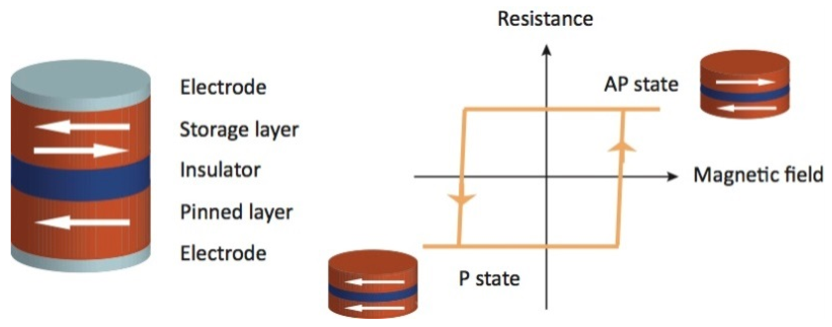
2.1. STT-MTJ

Bi-directional flowing of the write current is used in STT-MTJ. In order to have a successful operation, write current must be greater than the threshold current (or critical current) Ic0, so that the STT mechanism allows MTJ to perform magnetism switching between parallel and anti-parallel states. Physically-based MTJ compact models have been realized in [27]:
I C 0 = α γ e μ B g ( μ 0 M S ) H K V = 2 α γ e μ B g E
where Hk is the effective anisotropy field, μ0 is free space permeability, Ms is the saturation magnetization, a is the constant of magnetic damping, g is the ratio of gyromagnetic, e is the elementary charge, V is the volume of the free layer, μB, g and E are the Bohr magneton, the factor of spin polarization efficiency and the energy of oxide barrier, respectively. The average switching probability and switching operation time τ1 could be expressed by
Pr ( t pulse ) = 1 exp ( t pulse τ 1 )
1 τ 1 = [ 2 C + ln ( π 2 Δ ) ] μ B P em ( 1 + P 2 ) ( I write I C 0 )
where tpulse is the write current pulse duration, C is Euler’s constant, ∆ is the thermal stability factor, m is the magnetization moment, and P is the tunneling spin polarizations. MTJ with a high TMR can guarantee easy access to peripheral CMOS blocks, e.g., sensing and control circuits [28,29,30,31,32]. The real value of TMR (TMR(V)) can be adjusted by changing zero bias (TMR(0)) and Vh (half of TMR(0)):
TMR(V) = TMR(0) (1 + V2/Vh2)−1

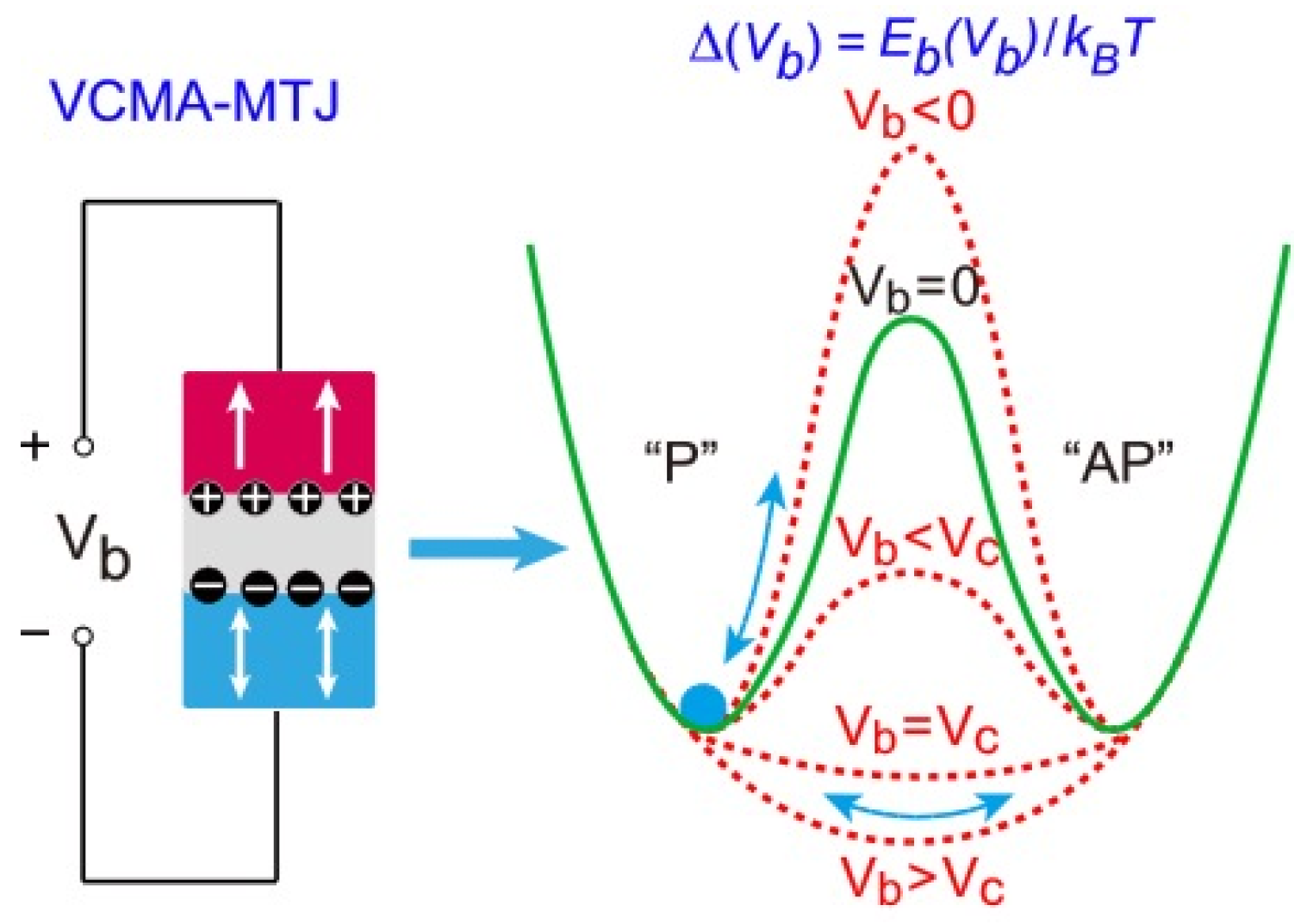
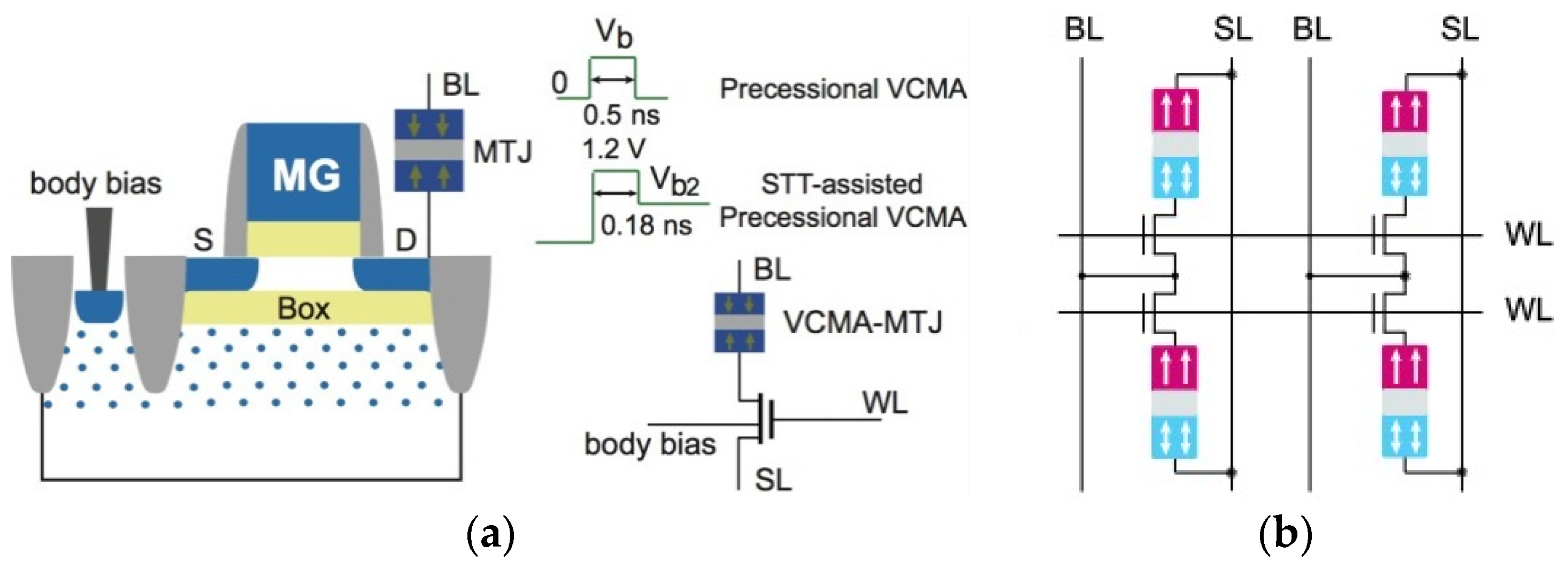
2.2. VCMA-Assisted Switching

Figure 2 illustrates a typical structure of VCMA-MTJ which is similar to that of PMA-STT-MTJ [25]. It is composed of two ferromagnetic layers sandwiched by an insulator as the oxide barrier. As the same as STT-MTJ, the resistance of the device is determined by magnetization orientations of the two ferromagnetic layers. In PMA-MTJ, the magnetization direction of one layer can be changed by sufficient current density (precessional switching) or sufficient pulse width (thermally-assisted switching) flowing through it while that of the other is fixed. By using the VCMA mechanism, the external voltage (or electric field) can modulate the interfacial PMA of CoFeB/MgO stacks [20]. With this effect, a positive (negative) voltage can reduce (increase) interfacial PMA.
Figure 2 illustrates a typical structure of VCMA-MTJ which is similar to that of PMA-STT-MTJ [25]. It is composed of two ferromagnetic layers sandwiched by an insulator as the oxide barrier. As is also the case for STT-MTJ, the resistance of the device is determined by the magnetization orientations of the two ferromagnetic layers. In PMA-MTJ, the magnetization direction of one layer can be changed by a sufficient current density (precessional switching) or sufficient pulse width (thermally-assisted switching) flowing through it, while that of the other is fixed. By using the VCMA mechanism, the external voltage (or electric field) can modulate the interfacial PMA of CoFeB/MgO stacks [20]. With this effect, a positive (negative) voltage can reduce (increase) interfacial PMA.
As shown in Figure 2, the impact of voltage amplitude (Vb) on the VCMA-MTJ is explained as follows: thermally assisted switching is realized with low positive voltage (0 < Vb < Vc) and a reduced energy barrier. Alternatively, precessional VCMA switching is achieved by way of a high positive Vb, which is greater than Vc, to eliminate the energy barrier (Eb). When Vb is lower than 0 V, the negative voltages can be used to strengthen the Eb.
From the aspect of energy levels, the stable magnetization states of the free layer in a PMA-MTJ device are divided by Eb which is modeled as a function of the applied voltage [23]. The voltage dependent ∆(Vb) is obtained:
∆(Vb) = Eb(Vb)/kBT = ∆(0) − ξAVb/kBTtox
where ∆(0) is the thermal stability (zero voltage), ξ is the coefficient to weigh the PMA at Vb, tox is MTJ oxide layer thickness, A is the MTJ sectional area, kB and T are the Boltzmann constant and temperature respectively. As demonstrated in Figure 2, by setting ∆(Vb) = 0, Vc as the minimum voltage of VCMA effect can be estimated by:
Vc = ∆(0)kBTtox/ξA
which is used to entirely eliminate the energy barrier of the MTJ. When a Vb (positive) is greater than Vc, Eb can be entirely eliminated so that the magnetization of the free layer becomes unstable and precessionally oscillates between the two stable states (referred as precessional switching regime). Alternatively, with the amplitude of the voltage inferior to Vc, the energy barrier is lowered, where the thermally-activated switching regime can be realized in this domain. Due to the thermal activation, the Mz has the possibility to be damped back to the initial, or to be changed to the other state. MTJ operated in this regime can rely on an extra magnetic field or a switching current to improve the switching efficiency (donated as STT-assisted precessional VCMA).
Moreover, if switching occurs at the precessional switching regime, a precise control of the voltage pulse duration or additional write-verify algorithms are generally necessary to guarantee the success of MTJ switching [33]. Table 2 lists the physical parameters of STT-MTJ and VCMA-MTJ used in this paper. The STT-MTJ and VCMA-MTJ compact model proposed in [25,34] is employed in the next section.

3. High Performance MRAM Writing

In general, MRAM is implemented based on a hybrid magnetic/CMOS architecture. The main MRAM array architectures, e.g., 1T-1MTJ and cross-point, have been reported in [14,35,36]. In the classic 1T-1MTJ array (see Figure 3), MTJ locates in series with the access transistor, where gate is connected to the word-line (WL), drain to the bit-line (BL) crossing the MTJ and source to the source-line (SL). Once non-volatile data is stored the MRAM array, and a sense amplifier (e.g., pre-charge SA) is required for the read operation [35,36,37,38]. Other assisted blocks (e.g., write control circuit, voltage pulse controller in VCMA-MTJ) are needed as well.
In this section, a PMA-STT-MTJ [34] compact model, a VCMA-MTJ compact model [25] and a 28 nm CMOS design-kit (ultra-thin body and buried oxide fully depleted silicon-on-insulator, UTBB-FD-SOI) are utilized to study MRAM writing performance. The design space of MRAM writing is explored with energy versus switching delay. Reliability issues including process variation, dielectric breakdown and thermal stability are discussed.

3.1. MRAM Writing

In this work, three MTJ switching methods —traditional STT, the precessional VCMA mechanism and STT-assisted precessional VCMA—are investigated with 1T-1M MRAM architecture. Figure 4 illustrates the simulation waveform with related MTJ compact model. Increased switching voltage can guarantee successful writing. The writing latency can be improved with an energy consumption tradeoff. However, in VCMA strategy, switching errors can be associated with if the Vb amplitude lasts too long (e.g., tb is greater than 0.8 ns), where the state of VCMA-MTJ has the risk of switching back to the initial one.
As shorter or longer voltage pulse duration may lead to reduced switching probability and cause switching failure, a precise control of the voltage pulse amplitude and duration can guarantee successful VCMA switching. Another requirement of the precessional VCMA strategy is the usage of an external magnetic field, which increases design complexity and energy consumption for MRAM applications.

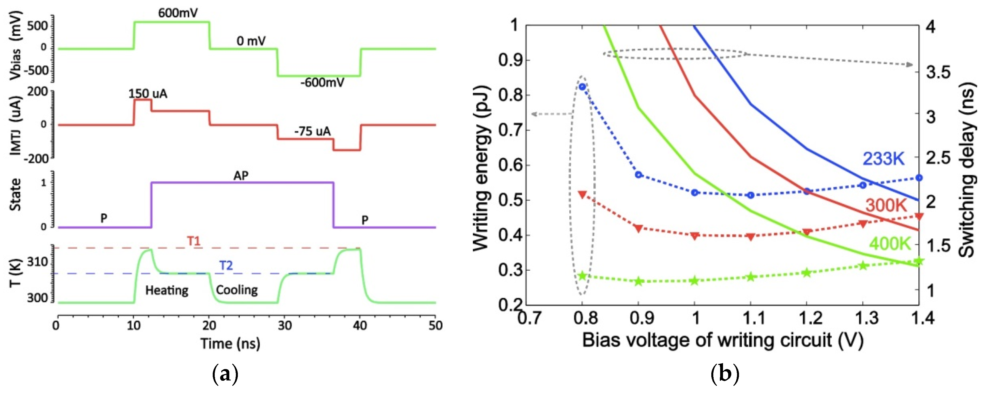
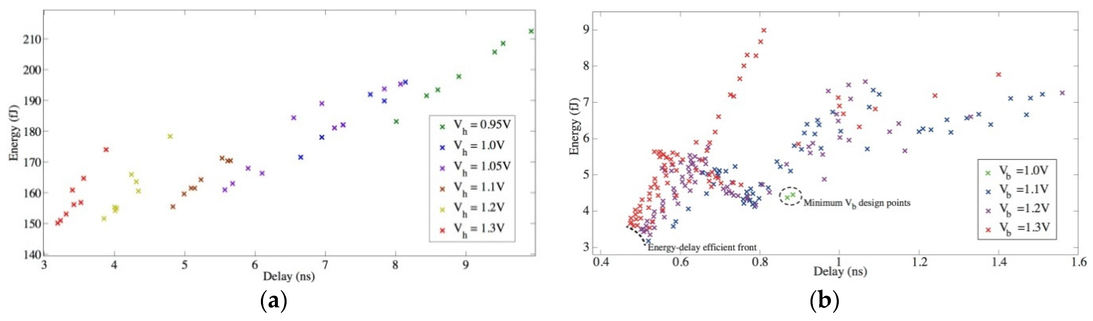
3.2. Energy Efficiency

VCMA-MTJ switching performance is dependent on transistor sizing (W/L), VCMA pulse duration and pulse amplitude. Compared to traditional STT-MTJ magnetization switching, an electric field is used in the VCMA effect to replace electric current, which significantly lowers the dynamic power consumption. Leakage power consumption in VCMA-MTJ is negligible because much thicker tunneling barrier is used. A VCMA pulse is normally-off (with 0 V pulse amplitude) during idle and MTJ-sensing operation.
Access transistor sizing strategy, VCMA pulse duration and pulse amplitude scaling are investigated. The energy–delay efficiency of VCMA switching is studied within the 1T-1MTJ circuit. Figure 5 illustrates STT-MTJ and VCMA-MTJ switching energy-delay efficient front and design space. In STT-MTJ, minimum 0.95 V writing amplitude is required to have a successful writing operation. In Figure 5b, minimum energy (3.18 fJ/bit) is realized with access transistor W = 400 nm, Vb = 1.1 V and tb = 0.44 ns. Minimum delay is achieved with W = 400 nm, Vb = 1.3 V and tb = 0.38 ns.
Table 3 compares the achieved energy point with different CMOS technology nodes. Comparing with the VCMA-MTJ reported in 32 nm PTM and 40 nm bulk-CMOS, the minimum energy per 1-bit of non-volatile data writing are improved by 68.5% and 48.2%, respectively, with 28 nm FD-SOI CMOS implementation. Although STT-MRAM is an outstanding alternative memory of conventional SRAM, the memory density and writing efficiency still need to be improved [39].

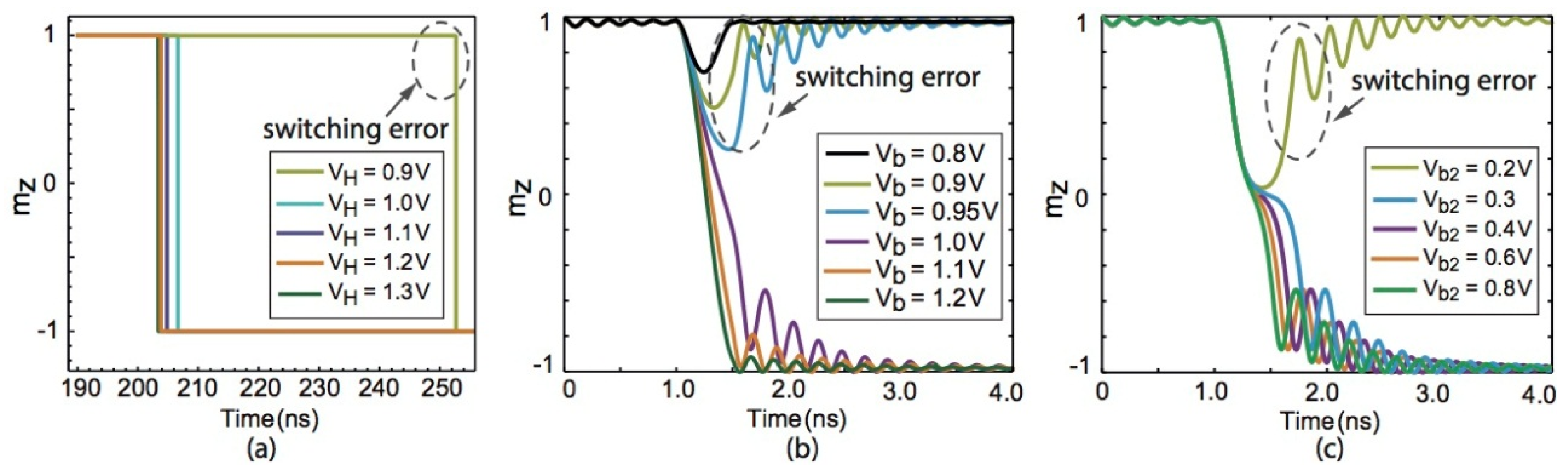
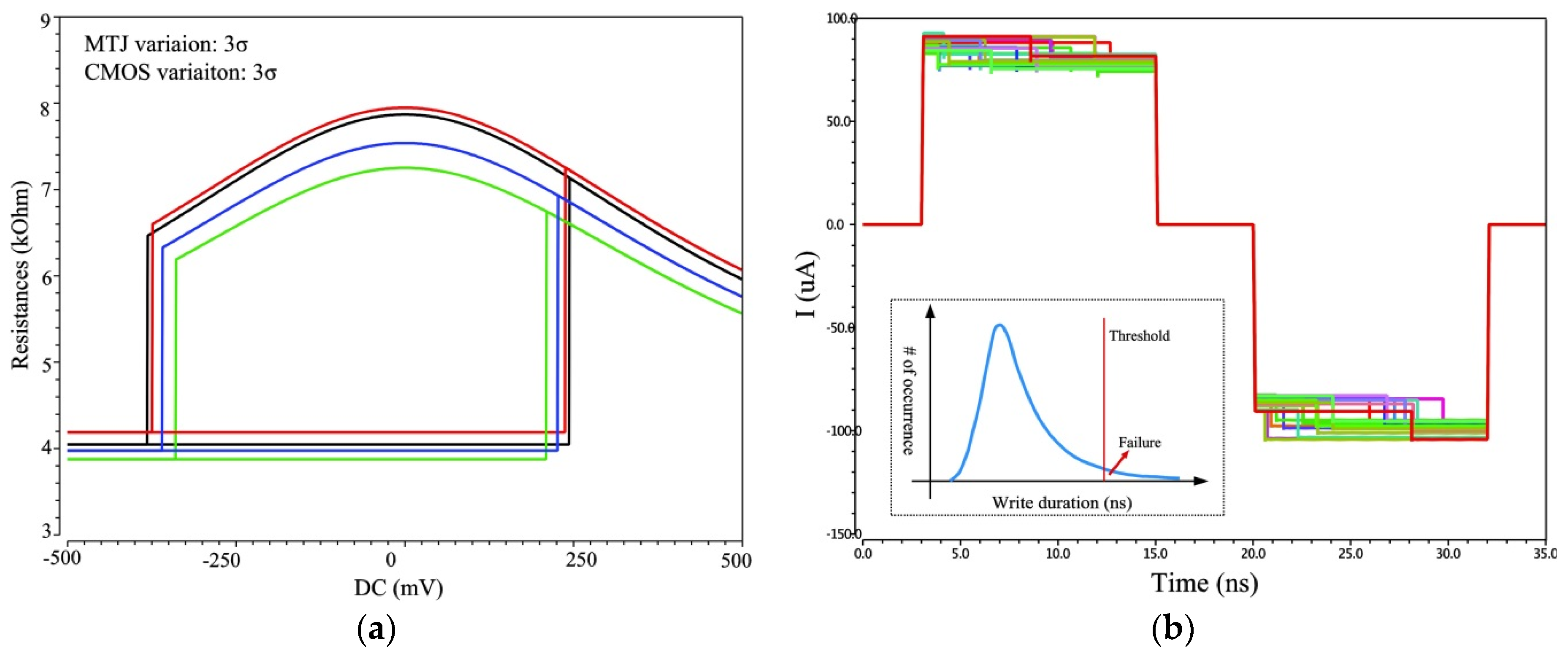
3.3. Stochastic Effects

Based on MTJ theoretical models and several experimental measurements [40,41,42], the MTJ switching procedure can be realized as a stochastic progress because of the thermal fluctuations of magnetization. MTJ switching latency is not deterministic but follows a statistical range. Reliability issues such as write uncertainties and switching errors must be overcome in MRAM applications. This switching probability is dependent on pulse width and amplitude. For VCMA-MTJ, with appropriate write voltage (e.g., 1.075 V to 1.125 V), a switching can be completed in 700 to 800 ps pulse with error rate <10−10 [42].
MTJ stochastic effects can be used as a physical random source for cryptography and security circuits; e.g., stochastic computing, approximate computing and true random number generator [43,44,45]. Compared with the conventional CMOS-based True Random Number Generators (TRNGs), the magnetic device-based technology designs can effectively achieve a simple structure, a more compact area, a higher speed and better energy efficiency. However, the process variations of MTJ and transistors have not been taken into account in these designs; other peripheral circuits are not considered, and thus the robustness remains doubtful [43].

3.4. Reliability Issues

With the continuous scaling of CMOS technology nodes, MRAM with design-for-reliability is required due to the impacts of parametric process variations, aging mechanisms and transient faults [35,36,45,46,47,48]. In this section, the process variation, thermal variation and breakdown are reviewed for reliable MRAM design.

3.4.1. Process Variation

The MTJ switching mechanism has been demonstrated to be intrinsically stochastic, which has been validated by experimental work [40,41,42]. On the other hand, due to the limited fabrication precision, the development of submicron CMOS transistors and nanometer-level MTJ devices suffer from parametric process variations. Due to these effects, the switching failure takes place frequently in both MTJ writing (e.g., fails to store the right data) and sensing (e.g., unexpected switching) phases.
In order to study the process variation, physical parameters are stochastically modeled. For MTJ devices, the deviations of oxide barrier thickness, free layer thickness and TMR ratio are modeled with Gaussian distribution with 3σ range. For CMOS transistor, its compact model is analyzed simultaneously with MTJ compact model to realize hybrid magnetic/CMOS circuit performance. Figure 6 demonstrates the DC simulation and Monte Carlo transient simulation. Write errors may occur if the write duration is less than the required value.

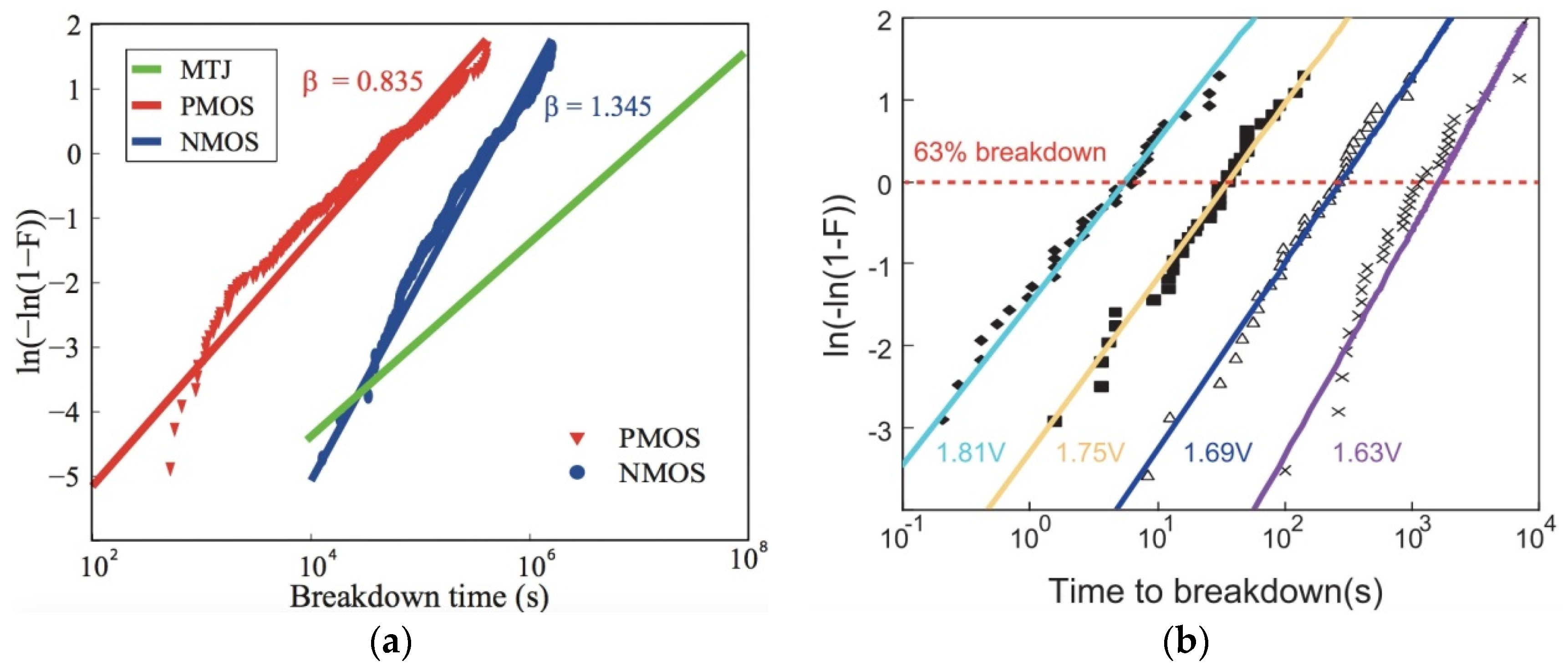
3.4.2. Dielectric Breakdown

High current flowing or voltage pulse is usually required to guarantee MTJ switching. The high electric field and significant self-heating effect cause a risk of dielectric breakdown in MTJ oxide barrier, which lead to MTJ dielectric breakdown, as well as performance degradation (by soft breakdown) and functional failure (by hard breakdown) of hybrid CMOS/MTJ circuits.
The MTJ oxide barrier thickness is lower than FD-SOI CMOS oxide, which is around 1 nm [46]. The probability of breakdown occurrence in CMOS devices follows the Weibull distribution [47]. Figure 7 illustrates the breakdown probability with operation time duration of MTJ and nNOS/pMOS transistors. The curves of FD-SOI transistors show agreement with the experimental data in [47]. The stress voltage applied on MTJ oxide barrier is around 400 mV, whereas CMOS transistor is biased with 1 V gate voltage.
High stress voltage facilitates the switching but induces short time to breakdown. Thus, an optimum tradeoff of power design can be obtained according to the requirements of writing probability and endurance [49].

3.4.3. MTJ Thermal Stability

The thermal fluctuation affects deeply the MTJ characteristics and hybrid MTJ/CMOS circuit performance [34]. During the MRAM writing phase (see Figure 8a), the temperature increases from the initial value to high, and then falls when the MTJ switching is completed. The maximum value of temperature saturation is dependent on MTJ parallel and antiparallel states.
As depicted in Figure 8b, an increased operation temperature (e.g., 400 K) results in faster and lower power writing processes, but accelerates the MTJ hard breakdown, which leads to a shorter time to failure. Thus, designers must pay attention to the tradeoff of energy consumption, temperature fluctuation, as well as the MTJ endurance.

4. Discussion

The development of MRAM still encounters bottlenecks in dynamic power consumption, energy–delay efficiency and reliability issues. VCMA-MTJ-based MRAM enables designers to have a chance to utilize a controlled electric field (or a voltage) for magnetization switching with efficient non-volatile writing and robust writing process control.
Compared to STT-MTJ based MRAM, the precessional VCMA mechanism and STT-assisted methods achieve a faster writing speed and lower power consumption. The dynamic writing energy can be reduced to 3.2 fJ/bit, whereas STT-MTJ MRAM has ×30 larger energy consumption. In particular, the STT-assisted precessional VCMA strategy is less complex compared to precessional VCMA, because an external magnetic field and precise pulse duration control are no longer needed.
One possible problem about VCMA-MTJ-based MRAM is the source degeneration of the access transistor [25], as the MTJ parallel and antiparallel resistance (100 kΩ Rp and 200 kΩ Rap) is larger than previous STT-MTJ. In precessional VCMA-MRAM, the positive pulse only stresses from bit-line to source-line with the unipolar VCMA effect; therefore, the source degeneration is not dominant. However, in STT-assisted VCMA-MRAM, the bipolar STT current may induce current driving degradation in MRAM access transistor when the current flow from source-line to bit-line.
Fortunately, after applying the VCMA voltage, the magnetization of MTJ free layer is precessionaly oscillating around the effective field. Only a small driving current can break the equilibrium and switch the magnetization. Therefore, a small current density is provided by the access transistor and source degeneration can be designed with tolerance.
The reliability of hybrid CMOS/magnetic integration is a major concern for circuit designers in the near future [43,44,45,46,47,48,49]. The integration of unreliable, deep-scaled nanometer CMOS and MTJ processes pose tremendous challenges from the device level up to system level. The design margins to guarantee reliable MRAM write and read operations are no longer sufficient and result in huge circuit overdesign. Our future work will focus on yield and aging performance evaluation of VCMA-MTJ-based MRAM circuits.

5. Conclusions

In this work STT-MTJ and VCMA-MTJ have been investigated for next-generation low power nonvolatile working memory applications. By using physical MTJ compact models, design space exploration was executed by considering write pulse amplitude and duration, as well as access transistor sizing and layout area, in both STT-MTJ and VCMA-MTJ-based MRAM. Improved energy-delay performance can be realized in a 28 nm UTBB-FD-SOI technology. Two VCMA strategies—the precessional and STT-assisted precessional methods—show improved performance in writing energy consumption and latency compared to traditional STT-MTJ writing. Reliability issues, e.g., process variations, dielectric breakdown and thermal stability, have been discussed. Reliability in VCMA-MTJ-based hybrid CMOS/magnetic integration will be emphasized in our future work.

Acknowledgments

This work is supported by program Nano2017/SOBER. This work is also supported by National Natural Science Foundation of China (Grant No. 61474022) and National High Technology Research and Development Program 863 (Grant No. 2015AA016601).

Author Contributions

H.C. organized this work. H.C., W.K., Y.W. performed the modeling and analysis. The manuscript was written by H.C. and edited by all authors.

Conflicts of Interest

The authors declare no conflict of interest.

References

  1. Chappert, C.; Fert, A.; Van Dau, F.N. The emergence of spin electronics in data storage. Nat. Mater. 2007, 6, 813–823. [Google Scholar] [CrossRef] [PubMed]
  2. Baibich, M.N.; Broto, J.M.; Fert, A.; Van Dau, F.N.; Petroff, F.; Etienne, P.; Creuzet, G.; Friederich, A.; Chazelas, J. Giant magnetoresistance of (001)Fe/(001)Cr magnetic superlattices. Phys. Rev. Lett. 1988, 61, 2472–2475. [Google Scholar] [CrossRef] [PubMed]
  3. Binasch, G.; Grunberg, P.; Saurenbach, F.; Zinn, W. Enhanced magnetoresistance in layered magnetic structures with antiferromagnetic interlayer exchange. Phys. Rev. B 1989, 39, 4828–4830. [Google Scholar] [CrossRef]
  4. Julliere, M. Tunneling between ferromagnetic films. Phys. Lett. A 1975, 54, 225–226. [Google Scholar] [CrossRef]
  5. Gallagher, W.J.; Parkin, S.S.P. Development of the magnetic tunnel junction MRAM at IBM: From first junctions to a 16-Mb MRAM demonstrator chip. IBM J. Res. Dev. 2006, 50, 5–23. [Google Scholar] [CrossRef]
  6. Nozieres, J.; Dieny, B.; Redon, O.; Sousa, R.; Prejbeanu, I. Magnetic Memory with a Magnetic Tunnel Junction Written in a Thermally Assisted Manner, and Method for Writing the Same; U.S. Patent Office: Washington, DC, USA, 2005. [Google Scholar]
  7. Slonczewski, J.C. Current-driven excitation of magnetic multilayers. J. Magn. Magn. Mater. 1996, 159, L1–L7. [Google Scholar] [CrossRef]
  8. Berger, L. Emission of spin waves by a magnetic multilayer traversed by a current. Phys. Rev. B 1996, 54, 9353–9358. [Google Scholar] [CrossRef]
  9. Ikeda, S.; Miura, K.; Yamamoto, H.; Mizunuma, K.; Gan, H.D.; Endo, M.; Kanai, S.; Hayakawa, J.; Matsukura, F.; Ohno, H. A perpendicular anisotropy CoFeB-MgO magnetic tunnel junction. Nat. Mater. 2010, 9, 721–724. [Google Scholar] [CrossRef] [PubMed]
  10. Liu, L.; Lee, O.J.; Gudmundsen, T.J.; Ralph, D.C.; Buhrman, R.A. Current induced switching of perpendicularly magnetized magnetic layers using spin torque from the spin hall effect. Phys. Rev. Lett. 2012, 109, 096602. [Google Scholar] [CrossRef] [PubMed]
  11. Liu, L.; Pai, C.-F.; Li, Y.; Tseng, H.W.; Ralph, D.C.; Buhrman, R.A. Spin-torque switching with the giant spin hall effect of tantalum. Science 2012, 336, 555–558. [Google Scholar] [CrossRef] [PubMed]
  12. Yu, S.; Chen, P.Y. Emerging memory technologies: Recent trends and prospects. IEEE Solid-State Circuits Mag. 2016, 8, 43–56. [Google Scholar] [CrossRef]
  13. Endoh, T.; Koike, H.; Ikeda, S.; Hanyu, T.; Ohno, H. An overview of nonvolatile emerging memories-spintronics for working memories. IEEE J. Emerg. Sel. Top. Circuits Syst. 2016, 6, 109–119. [Google Scholar] [CrossRef]
  14. Kang, W.; Zhang, Y.; Wang, Z.; Klein, J.-O.; Chappert, C.; Ravelosona, D.; Wang, G.; Zhang, Y.; Zhao, W. Spintronics: Emerging Ultra-Low-Power Circuits and Systems beyond MOS Technology. J. Emerg. Technol. Comput. Syst. 2015, 12, 42. [Google Scholar] [CrossRef]
  15. Duan, C.G.; Jaswal, S.S.; Tsymbal, E.Y. Predicted magnetoelectric effect in Fe/BaTiO3 multilayers: Ferroelectric control of magnetism. Phys. Rev. Lett. 2006, 97, 047201. [Google Scholar] [CrossRef] [PubMed]
  16. Weisheit, M.; Fähler, S.; Marty, A.; Souche, Y.; Poinsignon, C.; Givord, D. Electric field-induced modification of magnetism in thin-film ferromagnets. Science 2007, 315, 349–351. [Google Scholar] [CrossRef] [PubMed]
  17. Maruyama, T.; Shiota, Y.; Nozaki, T.; Ohta, K.; Toda, N.; Mizuguchi, M.; Tulapurkar, A.A.; Shinjo, T.; Shiraishi, M.; Mizukami, S.; et al. Large voltage-induced magnetic anisotropy change in a few atomic layers of iron. Nat. Nanotechnol. 2009, 4, 158–161. [Google Scholar] [CrossRef] [PubMed]
  18. Endo, M.; Kanai, S.; Ikeda, S.; Matsukura, F.; Ohno, H. Electric-field effects on thickness dependent magnetic anisotropy of sputtered MgO/Co40Fe40B20/Ta structures. Appl. Phys. Lett. 2010, 96, 212503. [Google Scholar] [CrossRef]
  19. Wang, W.G.; Li, M.; Hageman, S.; Chien, C.L. Electric-field-assisted switching in magnetic tunnel junctions. Nat. Mater. 2012, 11, 64–68. [Google Scholar] [CrossRef] [PubMed]
  20. Duan, C.G.; Velev, J.P.; Sabirianov, R.F.; Zhu, Z.; Chu, J.; Jaswal, S.S.; Tsymbal, E.Y. Surface magnetoelectric effect in ferromagnetic metal films. Phys. Rev. Lett. 2008, 101, 137201. [Google Scholar] [CrossRef] [PubMed]
  21. Shiota, Y.; Miwa, S.; Nozaki, T.; Bonell, F.; Mizuochi, N.; Shinjo, T.; Kubota, H.; Yuasa, S.; Suzuki, Y. Pulse voltage-induced dynamic magnetization switching in magnetic tunneling junctions with high resistance-area product. Appl. Phys. Lett. 2012, 101, 102406. [Google Scholar] [CrossRef]
  22. Han, G.; Huang, J.; Chen, B.; Ter Lim, S.; Tran, M. Electric Field Assisted Switching in Magnetic Random Access Memory. IEEE Trans. Mag. 2015, 51, 1–7. [Google Scholar] [CrossRef]
  23. Alzate, J.G. Voltage-Controlled Magnetic Dynamics in Nanoscale Magnetic Tunnel Junctions. Ph.D. Thesis, University of California, Los Angeles, CA, USA, 2014. [Google Scholar]
  24. Grezes, C.; Ebrahimi, F.; Alzate, J.G.; Cai, X.; Katine, J.A.; Langer, J.; Ocker, B.; Khalili, A.P.; Wang, K.L. Ultra-low switching energy and scaling in electric-field-controlled nanoscale magnetic tunnel junctions with high resistance-area product. Appl. Phys. Lett. 2015, 108, 012403. [Google Scholar] [CrossRef]
  25. Kang, W.; Ran, Y.; Zhang, Y.; Lv, W.; Zhao, W. Modeling and Exploration of the Voltage-Controlled Magnetic Anisotropy Effect for the Next-Generation Low-Power and High-Speed MRAM Applications. IEEE Trans. Nanotechnol. 2017, 16, 387–395. [Google Scholar] [CrossRef]
  26. Wang, S.; Lee, H.; Li, T.; Ebrahimi, F.; Amiri, P.K.; Wang, K.L.; Gupta, P. Comparative Evaluation of Spin-Transfer-Torque and Magnetoelectric Random Access Memory. IEEE J. Emerg. Sel. Top. Circuits Syst. 2016, 6, 134–145. [Google Scholar] [CrossRef]
  27. Worledge, D.C.; Hu, G.; Abraham, D.W.; Sun, J.Z.; Trouilloud, P.L.; Nowak, J.; Brown, S.; Gaidis, M.C.; OSullivan, E.J.; Robertazzi, R.P. Spin torque switching of perpendicular Ta/CoFeB/MgO-based magnetic tunnel junctions. Appl. Phys. Lett. 2011, 98, 022501. [Google Scholar] [CrossRef]
  28. Ikeda, S.; Hayakawa, J.; Ashizawa, Y.; Lee, Y.M.; Miura, K.; Hasegawa, H.; Tsunoda, M.; Matsukura, F.; Ohno, H. Tunnel magnetoresistance of 604% at 300 K by suppression of ta diffusion in CoFeB/MgO/CoFeB pseudo-spin-valves annealed at high temperature. Appl. Phys. Lett. 2008, 93, 082508. [Google Scholar] [CrossRef]
  29. Hanyu, T.; Endoh, T.; Suzuki, D.; Koike, H.; Ma, Y.; Onizawa, N.; Natsui, M.; Ikeda, S.; Ohno, H. Standby-Power-Free Integrated Circuits Using MTJ-Based VLSI Computing. Proc. IEEE 2016, 104, 1844–1863. [Google Scholar] [CrossRef]
  30. Kang, W.; Zhang, L.; Klein, J.-O.; Zhang, Y.; Ravelosona, D.; Zhao, W. Reconfigurable codesign of STT-MRAM under process variations in deeply scaled technology. IEEE Trans. Electron Device 2015, 62, 1769–1777. [Google Scholar] [CrossRef]
  31. Cai, H.; Wang, Y.; Naviner, L.; Zhao, W. Multiplexing Sense-Amplifier-Based Magnetic Flip-Flop in a 28-nm FDSOI Technology. IEEE Trans. Nmanotechnol. 2015, 14, 761–767. [Google Scholar] [CrossRef]
  32. Cai, H.; Wang, Y.; Naviner, L.; Zhao, W. Novel Pulsed-Latch Replacement in Non-Volatile Flip-Flop Core. In Proceedings of the IEEE Computer Society Annual Symposium on VLSI (ISVLSI), Bochum, Germany, 3–5 July 2017; pp. 57–61. [Google Scholar]
  33. Lee, H.; Alzate, J.G.; Dorrance, R.; Cai, X.Q.; Markovi, D.; Amiri, P.K.; Wang, K.L. Design of a fast and low-power sense amplifier and writing circuit for high-speed MRAM. IEEE Trans. Mag. 2015, 51, 1–7. [Google Scholar]
  34. Wang, Y.; Cai, H.; Naviner, L.; Zhang, Y.; Klein, J.-O.; Zhao, W. Compact thermal modeling of spin transfer torque magnetic tunnel junction. Microelectron. Rel. 2015, 55, 1649–1653. [Google Scholar] [CrossRef]
  35. Kang, W.; Li, Z.; Klein, J.-O.; Chen, Y.; Zhang, Y.; Ravelosona, D.; Chappert, C.; Zhao, W. Variation-tolerant and disturbance-free sensing circuit for deep nanometer STT-MRAM. IEEE. Trans. Nanotechnol. 2014, 13, 1088–1092. [Google Scholar] [CrossRef]
  36. Kang, W.; Zhang, L.; Zhao, W.; Klein, J.-O.; Zhang, Y.; Ravelosona, D.; Chappert, C. Yield and reliability improvement techniques for emerging nonvolatile STT-MRAM. IEEE J. Emerg. Sel. Top. Circuits Syst. 2015, 5, 28–39. [Google Scholar] [CrossRef]
  37. Cai, H.; Wang, Y.; Naviner, L.; Zhao, W. Low power magnetic flip-flop optimization with FDSOI technology boost. IEEE Trans. Mag. 2016, 52. [Google Scholar] [CrossRef]
  38. Cai, H.; Wang, Y.; Naviner, L.; Kang, W.; Zhao, W. Energy Efficient Magnetic Tunnel Junction Based Hybrid LSI Using Multi-Threshold UTBB-FD-SOI Device. In Proceedings of the Conference on Great Lakes Symposium on VLSI 2017 (GLSVLSI), Banff, AB, Canada, 10–12 May 2017; ACM: New York, NY, USA; pp. 23–28. [Google Scholar]
  39. Wang, K.L.; Lee, H.; Amiri, P.K. Magnetoelectric random access memory-based circuit design by using voltage-controlled magnetic anisotropy in magnetic tunnel junctions. IEEE Trans. Nanotechnol. 2015, 14, 992–997. [Google Scholar] [CrossRef]
  40. Devolder, T.; Hayakawa, J.; Ito, K.; Takahashi, H.; Ikeda, S.; Crozat, P.; Zerounian, N.; Kim, J.-V.; Chappert, C.; Ohno, H. Single-shot time-resolved measurements of nanosecond-scale spin-transfer induced switching: Stochastic versus deterministic aspects. Phys. Rev. Lett. 2008, 100, 057206. [Google Scholar] [CrossRef] [PubMed]
  41. De Castro, M.M.; Sousa, R.; Bandiera, S.; Ducruet, C.; Chavent, A.; Auffret, S.; Papusoi, C.; Prejbeanu, I.; Portemont, C.; Vila, L.; et al. Precessional spin-transfer switching in a magnetic tunnel junction with a synthetic antiferromagnetic perpendicular polarizer. J. Appl. Phys. 2012, 111, 07C912. [Google Scholar] [CrossRef]
  42. Wang, S.; Pal, S.; Li, T.; Pan, A.; Grezes, C.; Amiri, P.K.; Wang, K.L.; Gupta, P. Hybrid VC-MTJ/CMOS non-volatile stochastic logic for efficient computing. In Proceedings of the Design, Automation & Test in Europe Conference & Exhibition (DATE), Lausanne, Switzerland, 27–31 March 2017; pp. 1438–1443. [Google Scholar]
  43. Wang, Y.; Cai, H.; Naviner, L.; Klein, J.O.; Yang, J.; Zhao, W. A novel circuit design of true random number generator using magnetic tunnel junction. In Proceedings of the 2016 IEEE/ACM International Symposium on Nanoscale Architectures (NANOARCH), Beijing, China, 18–20 July 2016; pp. 123–128. [Google Scholar]
  44. Qu, Y.; Han, J.; Cockburn, B.F.; Pedrycz, W.; Zhang, Y.; Zhao, W. A true random number generator based on parallel STT-MTJs. In Proceedings of the Design, Automation & Test in Europe Conference & Exhibition (DATE), Lausanne, Switzerland, 27–31 March 2017; pp. 606–609. [Google Scholar]
  45. Cai, H.; Wang, Y.; Naviner, L.; Zhao, W. Robust Ultra-Low Power Non-Volatile Logic-in-Memory Circuits in FD-SOI Technology. IEEE Trans. Circuits Syst. I Regul. Pap. 2017, 64, 847–857. [Google Scholar] [CrossRef]
  46. Cai, H.; Wang, Y.; Naviner, L.; Zhao, W. Breakdown Analysis of Magnetic Flip-Flop With 28-nm UTBB FDSOI Technology. IEEE Trans. Dev. Mater. Reliab. 2016, 16, 376–383. [Google Scholar] [CrossRef]
  47. Saliva, M.; Cacho, F.; Ndiaye, C.; Huard, V.; Angot, D.; Bravaix, A.; Anghel, L. Impact of gate oxide breakdown in logic gates from 28nm FDSOI CMOS technology. In Proceedings of the 2015 IEEE International Reliability Physics Symposium, Monterey, CA, USA, 19–23 April 2015. [Google Scholar]
  48. Wang, Y.; Cai, H.; Naviner, L.; Zhang, Y.; Zhao, X.; Deng, E.; Klein, J.-O.; Zhao, W. Compact Model of Dielectric Breakdown in Spin-Transfer Torque Magnetic Tunnel Junction. IEEE Trans. Electron Device 2016, 63, 1762–1767. [Google Scholar] [CrossRef]
  49. Zhao, W.; Moreau, M.; Deng, E.; Zhang, Y.; Portal, J.-M.; Klein, J.-O.; Bocquet, M.; Aziza, H.; Deleruyelle, D.; Muller, D.; et al. Synchronous Non-Volatile Logic Gate Design Based on Resistive Switching Memories. IEEE Trans. Circuits Syst. I Regul. Pap. 2014, 61, 443–454. [Google Scholar] [CrossRef]
Figure 1. The magnetic tunnel junction (MTJ) consists of a storage layer and a pinned layer (separated by the insulator layer MgO). MTJ resistance is dependent on the orientation of MTJ magnetization with the parallel (P) and antiparallel (AP) states. The switching is operated by adjusting the magnetic field.
Applsci 07 00929 g001
Figure 2. Typical structure of the voltage-controlled magnetic anisotropy (VCMA)-MTJ device. The applied voltage amplitude (Vb) and critical voltage (Vc) determine the operation regimes of VCMA-MTJ: thermally assisted, precessional switching and STT-assisted precessional switching.
Applsci 07 00929 g002
Figure 3. (a) VCMA-MTJ based MRAM bit-cell with Fully Depleted Silicon-on-Insulator (FD-SOI) technology. Precessional switching is implemented with 0.5 ns pulse duration. STT-assisted processional method is implemented with a shorter (0.18 ns) pulse duration at 1.2 V Vb plus a lower Vb2 (e.g., 0.6 V). (b) Array structure of the MTJ based MRAMs.
Applsci 07 00929 g003
Figure 4. (a) STT-MTJ switching: low bias voltage may cause switching failure (e.g., VH = 0.9 V). (b) Precessional VCMA is implemented with a different Vb amplitude and 0.5 ns pulse duration. A minimum 1 V Vb is required to successful switch the MTJ. A decreased Vb amplitude could lead to longer switching latency. (c) Based on the setup of Figure 3a, at least 0.3 V Vb2 is required to complete STT-assisted precessional VCMA switching [25].
Applsci 07 00929 g004
Figure 5. Design space exploration with energy versus switching delay (a) STT-MTJ, (b) VCMA-MTJ.
Applsci 07 00929 g005
Figure 6. (a) DC simulations (4 times) of the perpendicular magnetic anisotropy (PMA) STT-MTJ/CMOS hybrid circuit to validate the correctness of the spice model, with 3 σ variations of both the MTJ and the CMOS access transistor. (b) Monte Carlo statistical simulation of the write operations: parallel (P) to anti-parallel (AP) and back to parallel (P). Write error may occur if the write duration is less than the required value.
Applsci 07 00929 g006
Figure 7. (a) The cumulative breakdown probability distribution in MTJ and 28-nm FD-SOI CMOS transistors [46]. Experimental results (fabrication and breakdown test from 28-nm FD-SOI CMOS) are demonstrated by the markers; (b) MTJ hard breakdown case study with 1.25 nm oxide barrier: Time-to-failure statistics at different stress voltages. The time value corresponds to 0 if Weibull function represents a 63% failure time [48].
Applsci 07 00929 g007
Figure 8. (a) Switching delay and energy consumed (dashed line) during writing process versus the bias voltage of STT-MRAM writing. (b) Cumulative breakdown probability distribution of 28-nm FD-SOI MOS devices and STT-MTJ [34].
Applsci 07 00929 g008
Table 1. Mainstream and emerging memory candidates which drive most of research [12,13,14].
MemorySRAMDRAMNOR-FlashNAND-flashSTT-MRAMPCRAMReRAMFeRAM 1
Cell area>100 F26 F210 F24 F2 (3D)6∼50 F24∼30 F24∼12 F215∼35 F2
Multi bit11231221
Supply<1 V<1 V>10 V>10 V<1.5 V<3 V<3 V<1.8 V
Read duration∼1 ns∼10 ns∼50 ns∼10 µs<10 ns<10 ns<10 ns<10 ns
Write latency∼1 ns∼10 ns10 µs–1 ms100 µs–1 ms<10 ns∼50 ns<10 ns<5 ns
RetentionN/A∼64 ms>10 y>10 y>10 y>10 y>10 y>10 y
Endurance>1016>1016>105>104>1015>109106∼10121013
Write energy∼fJ/bit∼10 fJ/bit∼100 pJ/bit∼10 fJ/bit∼0.1pJ/bit∼10 pJ/bit∼0.1 pJ/bit∼10 fJ/bit
1 SRAM, Static Random-Access Memory; DRAM, Dynamic Random-access memory; STT-MRAM, Spin Transfer Torque Magnetoresistive random-access memory; PCRAM, Phase-change Random-access memory; ReRAM, Resistive Random-access memory; FeRAM, Ferroelectric Random-access memory.
Table 2. Physical parameters in spin transfer torque (STT)-MTJ and voltage-controlled magnetic anisotropy (VCMA)-MTJ [25,26,34].
ParameterDescriptionSTT-MTJVCMA-MTJ
TMRTunnel magnetoresistance ratio150%100%
ToxMTJ oxide barrier thickness0.7 nm1.3 nm
Rp, RapMTJ resistance5 kΩ/12.5 kΩ100 kΩ/200 kΩ
TFLFree layer thickness1.2 nm1.19 nm
zThermal stability71.673.7
AreaMTJ layout surface24 F212 F2
W/LAccess transistor width/length 1300 nm/30 nm80 nm/30 nm
1 Access transistors are implemented with a 28 nm node Complementary Metal-Oxide-Semiconductor (CMOS) technology.
Table 3. Comparison of VCMA switching with different CMOS technology node.s
Design specification[39][26][25]This Work
Technology node32 nm CMOS 132 nm CMOS40 nm CMOS28 nm FD-SOI
Switching delay1–10 ns1.42 ns0.45 ns0.52 ns
Dynamic energy~100 fJ/bit10.1 fJ/bit6.14 fJ/bit3.18 fJ/bit
1 STT-MTJ-based magnetoresistive random access memory (MRAM) is used in this work. Others are realized with VCMA-MTJ based MRAM.

