Article

Self-Organized Nanoscale Roughness Engineering for Broadband Light Trapping in Thin Film Solar Cells

by
Carlo Mennucci
1,
Christian Martella
1,
Lucia V. Mercaldo
2,
Iurie Usatii
2,
Paola Delli Veneri
2 and
Francesco Buatier de Mongeot
1,*
1
Dipartimento di Fisica, Università di Genova, via Dodecaneso 33, I-16146 Genova, Italy
2
ENEA—Portici Research Center, Energy Technologies Department, Piazzale E. Fermi 1, 80055 Portici (NA), Italy
*
Author to whom correspondence should be addressed.
Appl. Sci. 2017, 7(4), 355; https://doi.org/10.3390/app7040355
Submission received: 3 March 2017 / Revised: 24 March 2017 / Accepted: 28 March 2017 / Published: 4 April 2017
(This article belongs to the Special Issue Light Management for Optoelectronics)

Abstract

:
We present a self-organized method based on defocused ion beam sputtering for nanostructuring glass substrates which feature antireflective and light trapping effects. By irradiating the substrate, capped with a thin gold (Au) film, a self-organized Au nanowire stencil mask is firstly created. The morphology of the mask is then transferred to the glass surface by further irradiating the substrate, finally producing high aspect ratio, uniaxial ripple-like nanostructures whose morphological parameters can be tailored by varying the ion fluence. The effect of a Ti adhesion layer, interposed between glass and Au with the role of inhibiting nanowire dewetting, has also been investigated in order to achieve an improved morphological tunability of the templates. Morphological and optical characterization have been carried out, revealing remarkable light trapping performance for the largest ion fluences. The photon harvesting capability of the nanostructured glass has been tested for different preparation conditions by fabricating thin film amorphous Si solar cells. The comparison of devices grown on textured and flat substrates reveals a relative increase of the short circuit current up to 25%. However, a detrimental impact on the electrical performance is observed with the rougher morphologies endowed with steep v-shaped grooves. We finally demonstrate that post-growth ion beam restructuring of the glass template represents a viable approach toward improved electrical performance.

1. Introduction

Thin film solar cell technologies, with the limited physical thickness of the light absorber, suffer from ineffective absorbance of near-bandgap light. To increase the photocurrent and then the power conversion efficiency, light harvesting strategies have to be introduced in order to trap the light in the active region while minimizing reflection and parasitic absorption. Based on the significant prospective benefits of reduced thickness, such as lower production costs and feasibility of materials with lower carrier diffusion length, the design of efficient light-management concepts is achieving more and more importance [1,2,3,4]. Both more mature technologies and the emerging families of polymer and perovskite solar cells can gain from the implementation of such strategies [5,6,7,8,9]. The need for light trapping is vital for the amorphous silicon based cells, both because of the weak absorption coefficient and for the limitations on the feasible thickness, due to the relatively poor electronic quality of the materials which calls for a drift-based p-i-n design [10]. Thanks to its maturity, this technology is thus often used as a platform for testing advanced approaches aimed at improving light management [3]. Here, a self-organized method for fabricating and tailoring nanostructured glasses to be applied as substrates promoting photon harvesting is presented and thin film silicon solar cells are once again used as the test-bed.
For thin film Si solar cells, the highest efficiencies have been so far reached with light-trapping schemes based on randomly textured interfaces combined with a reflective back contact. A common approach consists in the use of a rough front electrode made of textured transparent conductive oxide (TCO). Structuring of the supporting glass is also being pursued with nano-fabrication techniques such as nanoimprint lithography, where the desired morphology is reproduced into a UV-curable transparent resin [11]. Self-organized methods are an interesting alternative for patterning the substrates. As demonstrated in several seminal works [12,13,14], low-energy ion beam sputtering (IBS) has good potential as a single-step and fast processing route to produce large-area (size tunable), self-organized nanoscale patterned surfaces compatible with the present semiconductor industry. Ion irradiation of a self-organized metal nanowire (NW) stencil mask allows the projection of its morphological features into the supporting substrates which can be either amorphous, like glass [15], or crystalline, as GaAs and Silicon [16,17]. In the latter approach, high aspect ratio nanostructures are formed on the substrates as a consequence of the lower ion erosion rate of metal (e.g., gold) nanowires with respect to the substrate material. In order to further enhance the vertical amplification of transferred nanostructures, we developed an upgraded version of the process where the metal stencil mask lifetime is prolonged by co-evaporation of metallic atoms during ion irradiation (assisted-ion projection lithography, A-IPL) [18]. The high aspect ratio features confer broadband anti-reflection functionality to the textured glass substrate and at the same time ensure a high efficiency for diffuse scattering (high haze) [19,20].
We here pursued the goal of improving the tunability of the optical properties relying on the ability to control the morphological features of the pattern transferred from the metal stencil mask. To this purpose, the sacrificial mask has to be well-engineered and its morphological features have to be stable even under ion bombardment at high temperature (during A-IPL), where the gold is subjected to dewetting processes that can introduce disorder into the transferred pattern. In the present work, we demonstrate that we can separately optimize the pattern either for anti-reflective purpose or for high haze functionality by changing the lateral size of the nanostructures and their vertical scale in a controlled way. This has been achieved either by introducing a titanium adhesion layer between Au and glass during A-IPL process, or by prolonging the sample exposure to Au atom evaporation during Ar+ ion irradiation. The first method enables us to tune the lateral size of the Au nanowires employed as stencil mask, as well as improve their stability, thanks to the chemical and metallic bonding between glass and Au mediated by Ti. The second approach helps instead to enlarge the vertical scale and the volume of the nanostructures etched into the glass conferring excellent scattering properties to the surface. The potential of the nanostructured glass as advanced substrates for thin film solar cells has been finally tested by fabricating amorphous silicon devices. A possible approach for improving the electrical performance of the solar cells, seriously affected by the more roughened morphologies, is also reported.

2. Materials and Methods

The A-IPL nanostructuring technique was carried out in a UHV chamber equipped with a thermal evaporator and a defocused ion beam extracted from a gridded multi-aperture Ar+ source (Tectra instruments, Frankfurt, Germany). We evaporated 150 nm thick polycrystalline Au films [21,22] (average Au grains diameter around 100 nm and root mean square (RMS) surface roughness around 2 nm) on bare borosilicate glass or, in the experiments aimed to investigate the Ti role, on glass coated with 2 nm of evaporated Ti. The samples were subsequently exposed to defocused ion beam irradiation under grazing incidence conditions (ϑ = 82°), constant flux of 4.96 × 10¹⁵ ions cm−2·s−1 (measured in a plane orthogonal to the beam direction) and energy of 800 eV. The duration of the irradiation process was used as a control variable to determine the final ion fluence value. A biased tungsten filament (V = −13 V), providing electrons via thermionic emission, was placed close to the extraction grid in order to compensate surface charging effects due to ion irradiation.
The morphology of the samples was investigated ex situ by means of atomic force microscopy (AFM) operating in intermittent-contact mode (Nanosurf Mobile S and NanoMagnetic ezAFM) equipped with a high aspect ratio Si tip (ACLA by AppNano, Mountain View, CA, USA). The topography images were numerically analyzed by using WsXM software (Nanotec Electronica SL, Madrid, Spain) [23] in order to quantitatively evaluate the surface RMS roughness, the one-dimensional power spectral density functions (1D-PSD) and the height–height correlation functions, Hcf(r) [24].
In order to evidence the anti-reflective and scattering properties induced by the surface nanostructures, we performed far field optical reflectivity measurements by means of an integrating sphere (ISP-50-8-R from Ocean Optics, Dunedin, FL, USA) fiber coupled to a compensated deuterium–halogen lamp (DH-2000-BAL, Mikropak, from Ocean Optics, Dunedin, FL, USA) and to a high resolution solid state spectrometer (HR4000 from Ocean Optics, Dunedin, FL, USA). All spectra were normalized to the integrated reflectance signal of the standard reference sample (WS-1-SS-Spectralon from Ocean Optics, Dunedin, FL, USA).
The glass templates, prepared with different textured morphologies, were tested as novel substrates for thin film silicon solar cells. Identical amorphous silicon p–i–n single junctions were codeposited on nanostructured and flat glass for a meaningful comparison. A 750 nm thick RF-sputtered Al-doped ZnO (AZO) layer, with optical transmission ~80% and sheet resistance ~10 Ω/sq, was applied as a front transparent electrode. The p-i-n structure was made of a 7 nm thick p-type amorphous silicon-carbide layer, a 260 nm thick intrinsic amorphous silicon absorber layer, and a 30 nm thick n-type microcrystalline silicon layer. The silicon layers were deposited by plasma enhanced chemical vapor deposition (PECVD) in a commercial cluster tool; fabrication details are reported elsewhere [25]. On all the substrates, we finally applied 0.27 cm2 back reflecting contact pads made of 80 nm thick sputtered AZO, followed by a thermally evaporated Ag film. The devices were characterized by measuring the illuminated current-voltage (I-V) characteristic under the global air mass 1.5 (AM 1.5 G) spectrum with a WACOM class AAA dual-lamp solar simulator and the external quantum efficiency (EQE) with a Bentham PV300 (Bentham Instruments Ltd, Reading, UK) setup. The short-circuit current density (JSC) of the solar cells has been calculated from the EQE curves by convolution with the photon flux of the AM1.5 G solar spectrum, while the other parameters have been directly derived from the I-V curves. Total reflectance measurements were additionally carried out with the same setup described above.

3. Results

3.1. Self-Organized Nanopatterning

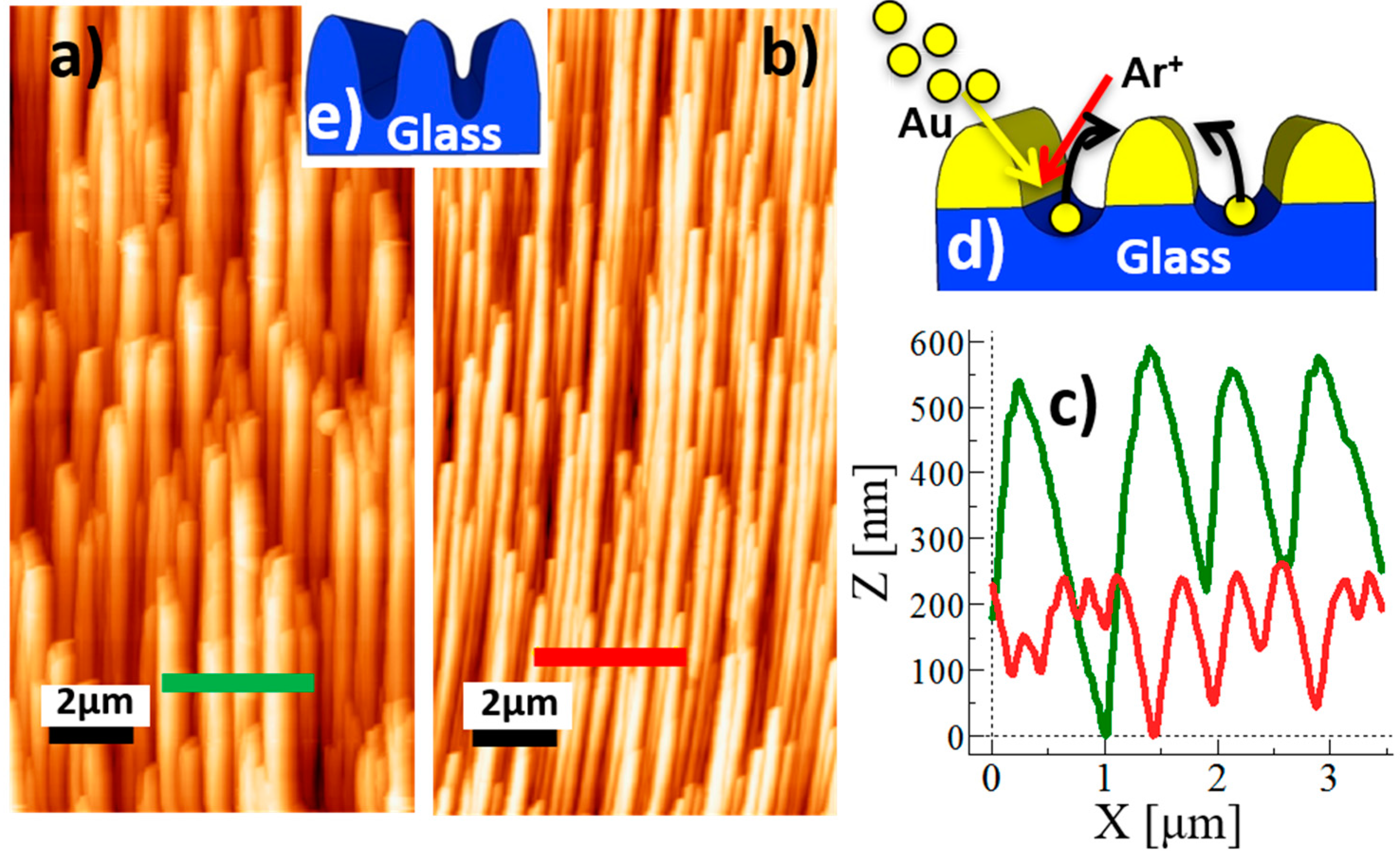
Light manipulation at the nanoscale relies on the ability to control morphological parameters of nanostructures. In our case, the nanofabrication process exploits in the first steps a self-organized array of Au nanowires which acts as a stencil mask. Under grazing incidence ion irradiation, an initially flat Au film develops a periodic ripple undulation at the metal-vacuum interface (Figure 1d). The ripple amplitude increases with ion dose while the residual thickness of the Au film decreases. When the bottom of the ripple valleys reaches the underlying glass, a disconnected array of nanowires is thus formed (Figure 1e). It acts as a stencil mask for etching the underlying substrate at later stages. Representative AFM topographies of Au nanowire stencil masks prepared either with (Figure 1a) or without (Figure 1b) a Ti adhesion layer interposed at the Au/glass interface show strong differences in statistical height; RMS roughness (σ) decreases from σ = 17 ± 2 nm to σ = 11 ± 2 nm when a Ti layer is employed. One can also notice that the longitudinal coherence and the order of the ripples are improved in nanowires synthesized with Ti layer and their lateral size is narrower, as shown by the topographic profiles superimposed in Figure 1c.
In order to quantitatively describe the role of titanium in the pattern formation process, we analyzed AFM morphological data in the framework of dynamic scaling theories, recurring to second order statistical quantities [26,27]. In the case of closely packed 1-dimensional nanostructures formed by IBS, one can easily derive the lateral scale of the structures from the lateral correlation length parameter, ξ, extracted from the Height-Height correlation function Hcf(r) = < [h(x+r)-h(x)]2 >. Hcf(r) has been systematically calculated for every AFM topographic line profile h(x), acquired along the fast scan direction which was kept orthogonal to ripple’s long axis. The data were cumulated and averaged over different AFM images acquired in equivalent areas in order to decrease statistical errors.
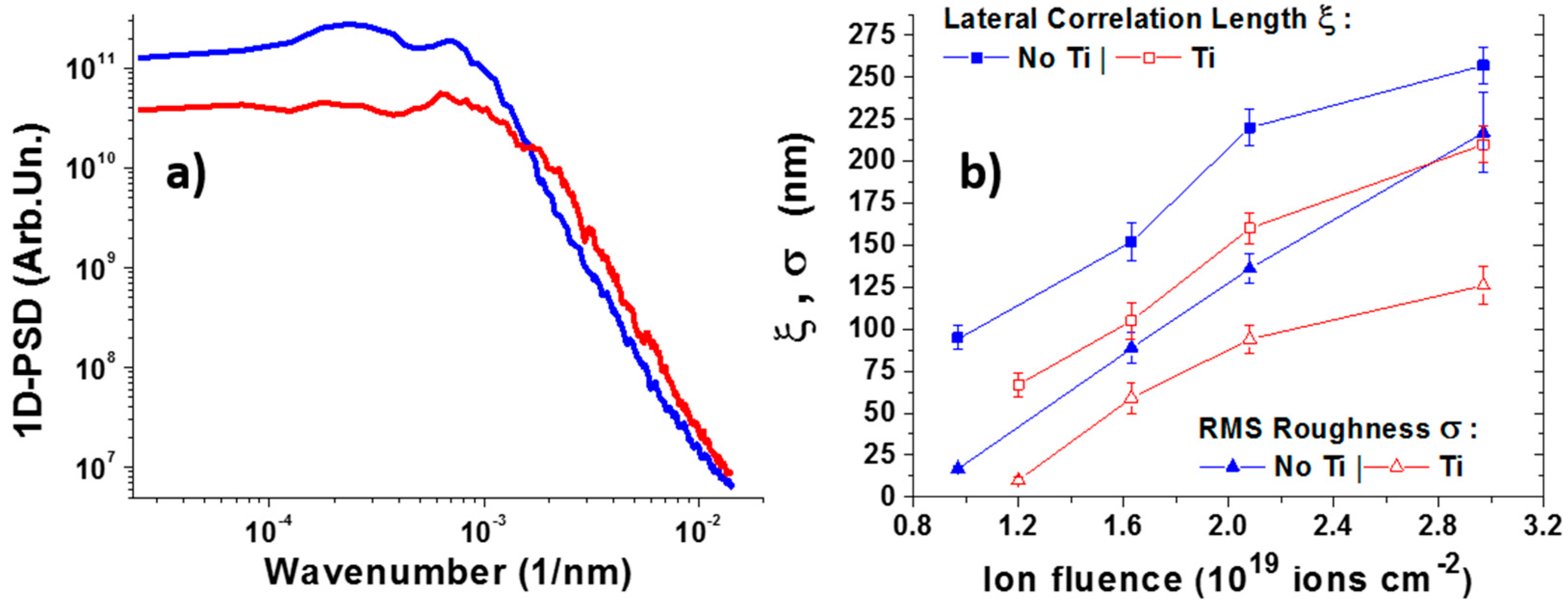
According to dynamic scaling theories for small values of the lateral displacement r, Hcf(r) follows a power law, while for large displacement values, Hcf(r) tends to a saturation value 2σ2, where σ is the RMS roughness [26,27]. The asymptotic break between the two regimes of Hcf(r) allows us to determine the statistical lateral correlation length, ξ, i.e., the distance r within which the surface height fluctuations are correlated. For distances r > ξ, the height variations are instead spread randomly [26,27]. In Figure 3b we report the lateral correlation length ξ extracted from the Hcf(r) as a function of the increasing ion fluence. In the case of Au nanowires mask it reads 95 ± 11 nm, while in presence of Ti this figure is reduced down to 65 ± 11 nm. The morphological differences introduced by Ti adhesion layer can be understood if we consider the role of Ti as an inhibitor of dewetting processes, either thermally activated or ion induced, thanks to the chemical and metallic bond of Ti with glass and Au respectively.
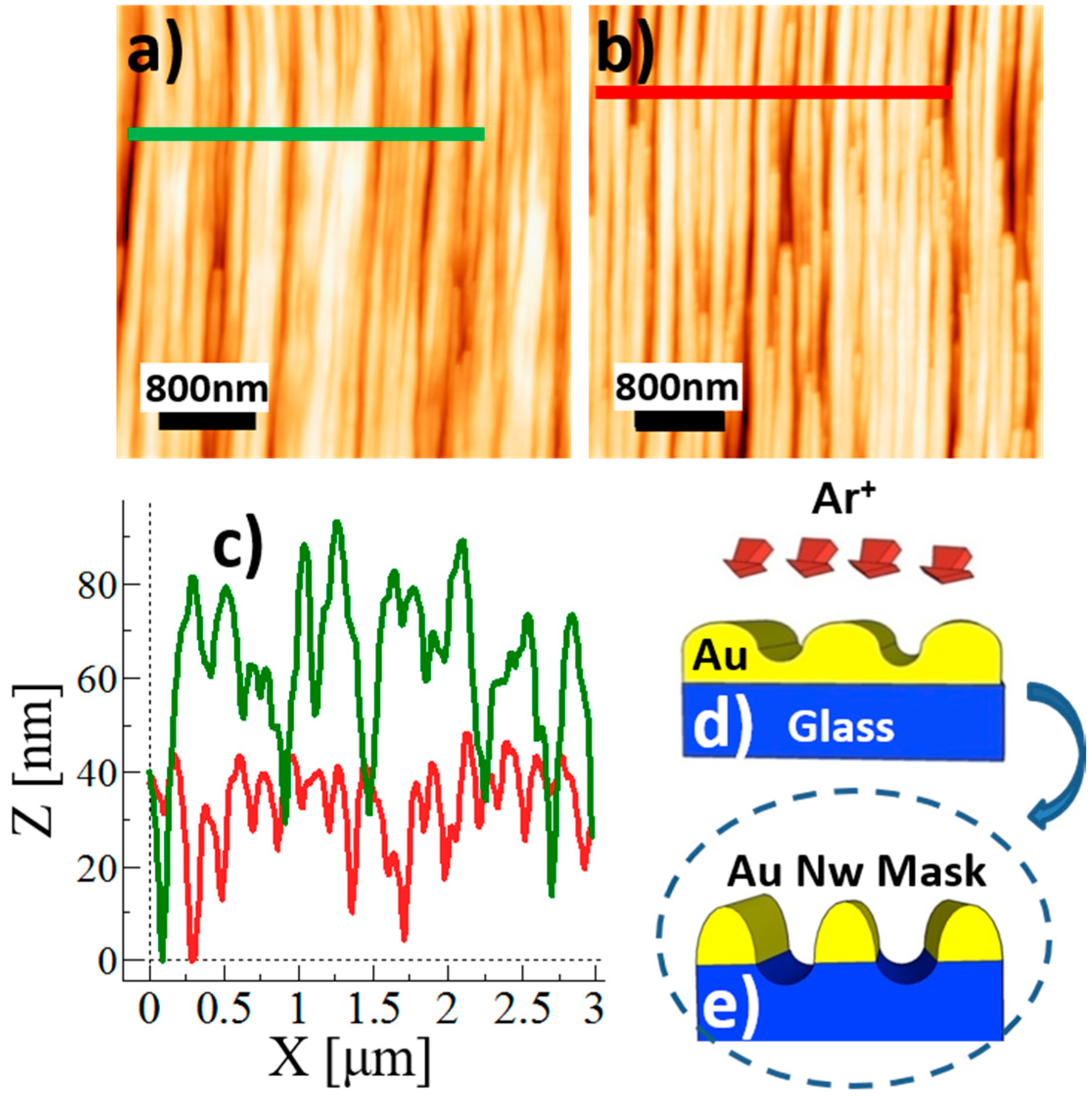
Once the Au nanowire array is formed, it acts as a stencil mask which guides selective etching of the underlying substrate in correspondence to the disconnected gaps. At this stage of the process the substrate is heated to 700 K and an auxiliary Au atom source is switched on (sketch in Figure 2d). The vertical scale of projected nanostructures is enhanced since Au adatoms evaporated on the heated surface can diffuse for longer distances until they reach the top of ripples, where they enrich the stencil mask and prolong its lifetime during ion irradiation. At the end of the process, the samples were further exposed to the ion beam until complete removal of the gold stencil mask was achieved. Further details on the A-IPL process can be found in reference [18].
In order to get high aspect ratio and tunable nanostructures capable of optical functionalization of the glass templates in terms of antireflection and light scattering effects [28,29], the A-IPL process has been applied to different stencil masks endowed with engineered morphologies presented in Figure 1. To this purpose, different substrates were prepared by A-IPL at T = 700 K and performed on the borosilicate glass with three different ion fluences: F1 = 1.63 × 10¹⁹ ions·cm−2, F2 = 2.08 × 10¹⁹ ions·cm−2, and F3 = 2.97 × 10¹⁹ ions cm−2, corresponding to Sample 1, Sample 2, and Sample 3, respectively. For the sake of simplicity, the samples synthesized at the same fluences, but with a Ti layer interposed between the glass and Au film, are named Sample 1-T, Sample 2-T, and Sample 3-T, respectively.
In Figure 2a,b the morphology of representative samples prepared respectively in the absence and in presence of titanium, for a given ion fluence (F2), are compared. Significantly, we can notice that in both cases the pattern transferred from the Au NWs mask into the glass exhibits an almost ten-fold vertical amplification. RMS roughness goes from σ = 17 ± 2 nm (11 ± 2 nm) to an average σ = 136 ± 9 nm (σ = 94 ± 8 nm) respectively without (with) Ti. Moreover, nanostructures synthesized in presence of Ti adhesion layer appear more elongated in the longitudinal direction and present a narrower lateral size, as shown by the comparison of line profiles in Figure 2c. In a more quantitative way, the lateral correlation length ξ reads 220 ± 11 nm for Sample 2, while we measure ξ = 160 ± 11 nm in presence of Ti (Sample 2-T).
In addition to the morphological tunability favored by Ti adhesion layer, we stress the broadband nature of the pattern presented in Figure 2a,b ensured by the presence of multiscale nanostructures organized in a pseudo-periodic array. Since diffractive properties are dependent on the Fourier spectra of the spatial frequencies, we calculated one dimensional power spectral densities (1D-PSD plotted in Figure 3a) from AFM data acquired on Sample 2 and 2-T, in similar manner to what was done for the Hcf(r) calculation.
Firstly, we highlight the broadband nature of the roughness distribution for both samples: a characteristic of paramount importance in view of optical broadband functionality required in PV applications; secondly, we also emphasize the peculiar behavior of Sample 2-T, which shows higher vertical amplification of surface features with large wavenumbers (small spatial wavelengths), while Sample 2 displays a strongly amplified roughness associated with small wavenumbers (large spatial wavelengths). This effect can be ascribed to the Ti layer presence which helps in preserving smaller structures on the sample and decreases coarsening effects.
Similar considerations also hold for the other couples of samples prepared at different ion fluences F1 and F3, which allow us to draw some conclusions on the general trend observed in the morphological data. In Figure 3b, the averaged statistical parameters σ and ξ of all samples, extracted from their Hcf(r) functions, are summarized as a function of the increasing ion fluence. For what concerns the amplification of σ and ξ with increasing fluences, a clear trend can be inferred.
RMS roughness σ and lateral correlation length ξ both increase by prolonging the ion dose during the A-IPL process. This increase of roughness at increasing ion fluences can be understood considering that the A-IPL process involves the use of an auxiliary gold evaporation source during the ion bombardment in order to prolong the shielding action of the Au nanowire stencil mask; in this way, the glass substrate is etched at deeper levels. This is confirmed by the strong increase of σ evident in Figure 3b, where points at a fluence lower than F1 = 1.6 × 10¹⁹ ions cm−2 are extracted from Au NWs mask topographies. The increase in lateral correlation length at higher fluences can be ascribed to the coarsening of the smaller scale spatial modulations due to the ion and thermally activated glass relaxation. In this way, ion fluence is an experimental parameter which gives us the opportunity to easily tune the morphology of nanostructured glasses and hence their optical properties.
On the other side, we also highlight that, for each explored ion fluence, the Ti adhesion layer allows us to decrease the average lateral scale and vertical extension of the nanostructures, expressed respectively by the statistical parameters ξ and σ (red open squares and triangles in Figure 3b). In particular, for the lowest ion fluence F1, the lateral correlation length of Sample 1-T measures 105 ± 11 nm; this value is compatible with the one registered on the Au ripple pattern before its decomposition in nanowires [18]. In the early stages of the A-IPL process the adhesion properties of the Ti layer are thus capable of stabilizing the Au nanowires stencil mask, preserving the small features present on the pristine Au ripple pattern.
The main physical mechanism is thus related to the inhibition of dewetting of the Au film once the continuous layer breaks up into an array of nanowires. The dewetting process is boosted by the hyperthermal energy deposition following ion impact which favours uphill mass transport of Au, thus exposing large portions of unshielded glass to harsh ion etching. This effect is manifested when the A-IPL process is prolonged at higher ion fluences F2 and F3, where the Au mask without Ti adhesion layer undergoes strong dewetting and allows the formation of large volume structures in the glass as a consequence of coarsening. In the presence of Ti instead, the pristine pattern of the Au continuous film is preserved and coarsening of the glass structures is prevented, resulting in more ordered and narrower glass ripples.
In this picture, the Ti adhesion layer thus represents a further experimental parameter (in addition to ion fluence), which allows to control the morphology of the nanopatterned substrates prepared by ion sputtering in the A-IPL configuration. The role of the engineered morphologies will be now explored from the optical point of view in order to elucidate their use in photon harvesting applications.

3.2. Optical Properties of Nanostructured Glasses

In order to characterize the optical performance of the nanostructured glass templates, we performed total integrated reflectance and haze measurements on the whole set of samples so far described (Samples 1, 1-T, 2, 2-T, 3, 3-T).
In Figure 4a we study the differential variation of the total integrated reflectance in the Vis-NIR range (450–1000 nm) of the nanostructured glass substrates normalized to a flat reference borosilicate glass, according to the equation |ΔR/R| = |(RnanoRflat)/Rflat|, where Rflat ≈ 8%. All of the diffuse reflectance measurements were carried out by means of an integrating sphere setup. The ΔR/R quantity describes the amount of anti-reflective effects present on nanostructured samples. Sample 2 and 2-T (blue squares and open triangles, respectively) reflect about 12% and 20% less light than a flat glass averaged on the whole Vis-NIR range of wavelengths. To summarize the information relative to all samples synthesized at different ion fluences, in Figure 4b (left scale) we plot the mean values of ΔR/R, integrated over the wavelength range Δλ = [450 nm; 1000 nm]. As the fluence is increased in the A-IPL process, the total reflectance raises towards the values of the flat glass and the antireflective effect vanishes. In particular, we observe an average reduction of reflectance from 23% (Sample 1-T) to 20% (Sample 2-T) to 6% (Sample 3-T-open red triangles). Correspondingly, for the samples without Ti, the average reduction of reflectance goes from 14% in Sample 1, to 5% for Sample 3 (blue squares). In other words, by modulating ion fluence one can control broadband anti-reflective effects, which are particularly enhanced in presence of the Ti layer.
Such behavior is in qualitative agreement with the “moth-eye” effect observed in bio-mimetic systems [30]. In fact, high aspect ratio corrugations, whose amplitude is a significant fraction of the incident light wavelength and whose lateral size is below the diffraction limit, allow us to gradually match the refractive indexes of substrate and air, leading to a suppression of reflectance (index-grading effect [29,31]).
The morphological analysis carried out on the six samples (Figure 3b) confirms that the Ti layer leads to the formation of more ordered patterns endowed with smaller scale non-diffractive features for photons belonging to the Vis-NIR spectrum. The observed index-grading anti-reflective behavior is predominant in Sample 1-T, which has the smallest correlation length in the range of 105 nm. We stress that these features can be useful for all kinds of applications in which a decrease of surface reflectivity is an important issue, as in de-trapping schemes employed in LED/OLED applications [32].
At a higher ion fluence, the lateral correlation length of the spatial corrugations increases due to coarsening: the importance of the moth-eye antireflection effect decreases and large angle diffuse scattering becomes predominant [21,33]. In view of light trapping applications employing the self-organized glass gratings, we stress that the scattering efficiency can be of predominant importance with respect to the anti-reflection behavior; enhanced light absorption in a PV device can in fact be achieved when scattered photons penetrate the absorber layer at the grazing angle and eventually are coupled to wave-guided modes by total internal reflection [34].
The scattering efficiency of the substrate, quantified as the ratio of diffuse reflectance to total reflectance (Haze), is determined experimentally by means of an integrating sphere. In Figure 4a, the haze signals measured on sample 2 (blue line) and 2-T (red-dashed line) are reported as a function of light wavelength. Haze values decrease from 60% to 45% (43% to 28%) in the wavelength range 450–1000 nm; a comparison with conventional Asahi-U reference substrates, measured in the same experimental condition, which exhibit haze values in the range 30%–2% [35] demonstrates the remarkable scattering efficiency of the novel substrates. The broadband scattering efficiency is high across the whole Vis-NIR spectrum and can be ascribed to the multiscale and pseudo-periodic nature of the self-organized structures highlighted in the reciprocal space spectral analysis (1D-PSD in Figure 3a and AFM data shown in Figure 2). The possibility to engineer the roughness spectrum of the nanostructured patterns, either by varying ion fluence or by adding a Ti adhesion layer, allows us to selectively enhance the scattering efficiency or the antireflective properties of the self-organized surfaces. The high haze of Sample 2 can be attributed to the presence of large scale spatial modulations which contribute to the 1D-PSD (Figure 3a blue trace) in the small wavenumber region below 1.5 × 10⁻³ nm−1. On the contrary, the moth-eye antireflective effect measured on Sample 2-T can be attributed to the presence of small scale structures, as witnessed by the cross-over of the 1D-PSD (Figure 3a red trace) observed in the large wavenumber region above 1.5 × 10⁻³ nm−1.
For what concerns the light scattering performance of the substrates prepared with different ion fluences, in Figure 4b (right scale) we summarize the average values of haze integrated over the whole spectral range (full and open circles refer to samples with and without Ti, respectively). One can notice that (i) higher haze values are observed for samples exposed to larger ion fluences; (ii) at fixed ion dose, haze is higher on the sample prepared without Ti adhesion layer. These observations can be rationalized in terms of the morphological evolution of the substrates with ion fluence summarized in Figure 3b. The RMS roughness and the lateral correlation length of the structures become larger (coarsening) as a consequence of dewetting of Au NWs mask, especially in absence of Ti. Due to coarsening, the dominant lateral size of the surface features grows at a point that scattering (haze) increases while index grading (moth-eye anti-reflective effect) decreases, as observed in the ΔR/R trace of Figure 4b.
A further aspect, of paramount importance for light trapping amplification in opto-electronic devices, is represented by the possibility to couple incoming light to wave-guided modes which confine propagation in the high refractive index layers formed by the substrate and absorber film [36,37].
In Figure 4d (see also sketch in Figure 4e), we directly visualize the presence of waveguided light which propagates laterally via internal reflection through the slab after being scattered at the textured glass interface. A light beam is propagated through the nanostructured glass slab in transmission geometry (pattern analogous to Sample 2), while the directly transmitted component is blocked by a beam stopper. Red dashed lines indicate the glass borders, while white dashed lines highlight the limits of the patterned area. Pictures have been taken from the top side in absence of ambient light, excluding the direct beam in order to avoid saturation of the camera. For the flat glass, Figure 4c, light is entirely transmitted in the direct beam (and thus blocked by the beam stopper). For the patterned glass, Figure 4d, light scattered perpendicularly to the ripple axis is guided for tens of millimeters through the slab by total internal reflection before leaking out and propagating to the detector.
We stress that the scattering and antireflective efficiency highlighted above are expected to be even more important when a high refractive-index material (e.g., silicon) is deposited on the nanostructured glass. In fact, the glass surface, texturized with a pseudo-periodic pattern, works as diffraction grating that can couple incident light to optical modes supported by the high-refractive index semiconductor layer, strongly enhancing its effective absorption [38].

3.3. Photon Harvesting in Thin Film Solar Cells

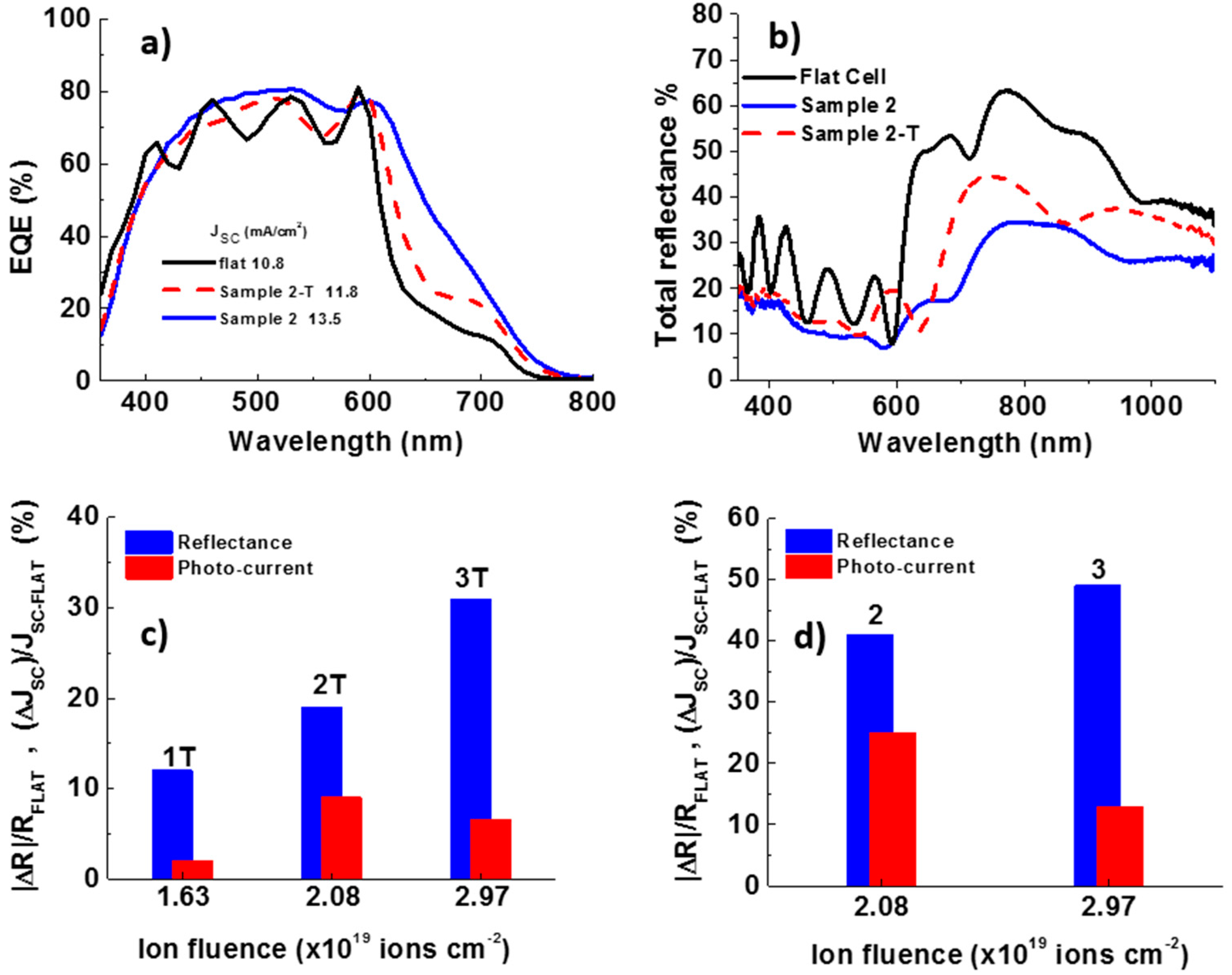
The optical performance of the patterned glass when applied as substrate for thin film solar cells has been investigated by fabricating p-i-n amorphous silicon solar cells and evaluating EQE and cell reflectance. The EQE measured for identical devices grown on flat and nanostructured substrates is shown in Figure 5a for Sample 2 and 2-T, which exhibited both antireflective and scattering effects. The response measured for both the rough cells is significantly enhanced when compared to the flat reference cell (black line). The EQE enhancement in the long wavelength range is indicative of efficient light trapping by means of multiple passes of scattered light within the absorber layer. In addition, a reduction of the interference fringes is observed, due to scattering from the uncorrelated roughness of the internal interfaces conformed to the pattern of the substrate. Quantitatively, JSC reaches 11.8 mA/cm2 and 13.5 mA/cm2 for Sample 2-T and 2, respectively, against 10.8 mA/cm2 for the flat cell. The total reflectance of the same solar cells is reported in Figure 5b. A significant reduction with respect to the flat case (black line) is measured for both the cells on textured glass and for Sample 2 in particular. This is in agreement with the results on the bare glass (Figure 4a), where Sample 2 is characterized by higher haze with respect to 2-T, which translates into a more effective light trapping in the solar cell. Similarly to what has been done for the bare glass substrates, we evaluated the relative variation |ΔR/R|cell = |RnanoRflat|/Rflat of the integrated reflectance over the full spectral range for the cells on different nanostructured substrates versus the flat cell. The latter parameter is shown as blue bars in Figure 5c,d, in order to quantify the efficiency of light handling within the cell. In general, a stronger reduction of reflectivity, i.e., improved light harvesting, is observed as the ion fluence increases, although for the samples without Ti adhesion layer (Figure 5d), only two cells are available. A further observation is that, for fixed ion dose, the cell without Ti has a better light harvesting efficiency. These results compare well with the characterization of the substrates shown in the previous section; as expected the light trapping efficiency scales progressively with samples endowed with higher haze.
Figure 5c,d also reports the corresponding relative enhancement of JSC measured for the same solar cells ΔJSC/JSC-flat. From Figure 5c, for the glasses obtained with Ti layer, it appears that this parameter increases with ion fluence, reaching a maximum for the intermediate value (Sample 2-T). For the largest fluence, on the other hand, the relative enhancement of JSC drops while the optical enhancement still increases. We attribute this divergent behavior to the monotonic increase of the RMS height of the nanopattern—as shown in Figure 3b—which likely does not guarantee the full conformal growth of the semiconductor layers of the cell due to shadowing effects, with formation of defective regions. In fact, this issue is also found for the cell on Sample 3, without Ti layer, and is confirmed by the low shunt resistance and reduced open circuit voltage measured in both cases (data not shown). The severe deterioration of the electrical performance likely disturbs the charge collection with impact on the EQE and JSC, thus masking the optical enhancement. It is known that high aspect ratio features, while valuable for an optical improvement, are usually detrimental to the electrical performance of the solar cells, as they can easily induce the formation of low-density faulty regions [2,38,39]; a trade-off between optical and electrical properties must thus be found.
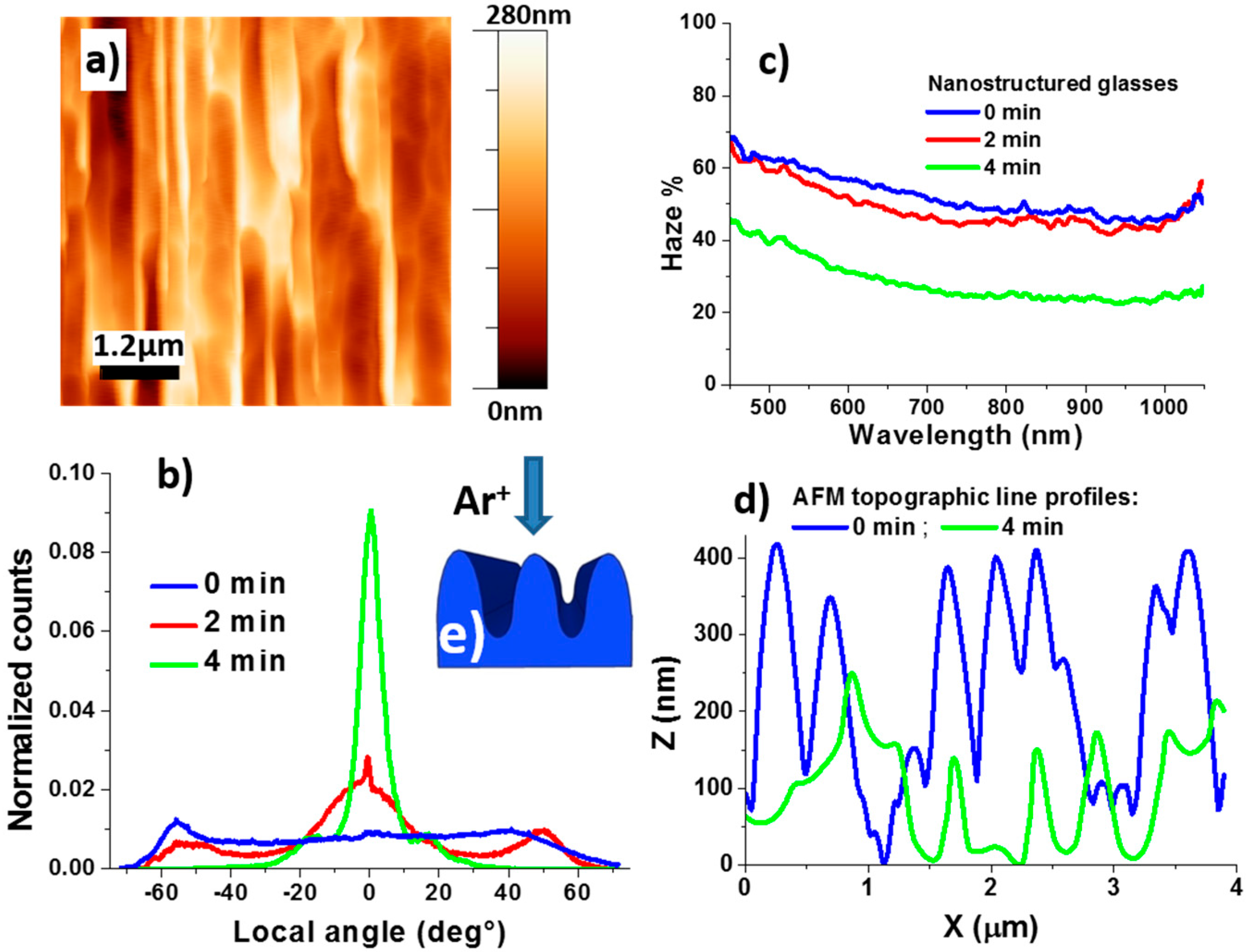
A post-growth refinement of the nanostructured glass morphology for improved electrical performance has been attempted via ion beam sputtering at normal incidence (normal-IBS), prior to solar cell deposition. The treatment exploits ballistic smoothening of the nanostructured surface [40]. We selected Sample 2 as a reference, since this substrate produced the largest JSC enhancement, while other relevant photovoltaic parameters where below the values obtained with the flat reference cell (e.g., open circuit voltage (VOC) reads 776 mV versus 840 mV for the flat cell). We synthesized three nanostructured glasses with morphology equivalent to Sample 2 and followed the evolution of the morphological properties after 2 min and 4 min of normal-IBS process (see sketch in Figure 6e). The pristine and the two treated glasses were finally used as substrates for co-deposited a-Si:H solar cells together, with a reference flat glass.
Figure 6 shows a morphological and optical comparison of the three samples. The high aspect ratio nanostructures typical of Sample 2 (see Figure 2a) are heavily smoothed by 2 min and 4 min cycles of normal-IBS treatment (the AFM image in Figure 6a refers to a 4 min cycle), and the V-shaped valleys typical of the pristine pattern are tailored to shallower U-shaped ones, as demonstrated by the superimposed AFM profiles in Figure 6d. The RMS roughness σ decreases from the initial value of ~150 nm, to 120 nm after 2 min of normal-IBS, and down to only 56 nm when doubling the treatment time. In order to gain insight into the smoothing mechanisms active with normal incidence ion irradiation, an analysis of the slope distribution of the AFM topography has been carried out. The first derivatives of the AFM images were computed orthogonally to the ripple axis and converted into normalized histograms of the local slope distribution (Figure 6b). For the pristine sample (blue line), the distribution is broad in the range of −60°/+60°. After 2 min of normal-IBS process (red line), a partial slope selection of the structures is observed, as evidenced by the two peaks in the distribution located approximately at −50° and +50°. A flattening effect in correspondence to the bottom of the U-shape valleys is evidenced by the growing peak around 0°. If the ion irradiation at normal incidence is protracted for 4 min (green line), the slope distribution is heavily impacted: the peak around 0° becomes dominant (strong smoothing effect) and two small peaks centered around ±15° are observed. The morphological reorganization is likely driven by the reduction of the surface free energy. It involves a smoothening of the corrugations caused mainly by ion induced relaxation mechanisms such as ion induced viscous flow, thermally activated surface self-diffusion, and ion induced surface diffusion [40]. Normal incidence IBS thus appears to be an effective and fast process for tailoring the glass morphology, competitive with respect to other plasma treatments implemented on the transparent conductive oxide [2,39].
The effect of the treatment on the light scattering properties of the glasses is severe after a 4 min process, since the haze parameter drops to values in the range 40% ÷ 20% across the spectral interval (Figure 6b). After a 2 min cycle, however, the haze maintains relevant values around 60% ÷ 50%, which qualifies the latter sample as a promising substrate for thin film solar cells.
Table 1 reports the photovoltaic parameters and relative variation of integrated reflectance of the co-deposited a-Si:H solar cells grown on the reference flat glass, on the pristine texture (0 min equivalent to Sample 2) and on treated nanostructured glass (2 min and 4 min). A relevant optical gain versus the flat reference is confirmed for the cells on pristine substrate and on the sample treated for 2 min (JSC above 13 mA/cm2 against 11.1 mA/cm2 for the flat case), while as expected the gain is negligible for the cell on the glass treated for 4 min (ΔJSC = 0.7 mA/cm2). The lowered light harvesting capability, as determined by the total reflectance measurements on the cells, confirms the effect of the smoothing treatment. The relative variation of integrated reflectance |ΔR|/Rflat of the cells decreases dramatically from 50% for the cell on the pristine texture down to only 2% for the sample treated for 4 min. Remarkably, for the sample treated with a 2 min cycle, the |ΔR|/Rflat value remains almost unchanged at around 40%, while the electrical performance is positively impacted. The electrical parameters of the flat reference cell are modest since the p-layer/TCO contact has not been adjusted to the AZO layer here in use as front electrode; nevertheless, the improving trend after the smoothening treatment is clear. For the cell on the pristine texture, a severe drop is measured both for VOC and FF (the latter caused by low shunt resistance), which can be ascribed to the V-shaped rough morphology of the substrate which prevents a conformal growth of the semiconducting layers. Conversely, the cells grown on treated substrates show a promising partial recovery of the electrical parameters. In particular ΔVOC, evaluated versus the flat cell, is reduced to ~60 mV (for the 2 min substrate) and ~10 mV (for the 4 min substrate), against ~150 mV for the cell on the pristine texture. The relevant mechanism is the adjustment of the local slopes. It has been shown, at least for microcrystalline Si, that V-shaped valleys with unfavorable opening angles—corresponding to slopes higher than 35° in our reference system—are prone to developing voids and fissures during the silicon layer growth, with a detrimental impact on VOC [39]. The almost complete VOC recovery achieved with the substrate treated for 4 min can thus be explained with the slope distribution fully constrained between ±35° (green line in Figure 6b). Further work is in progress to optimize the proposed treatment.
4. Conclusions

The morphological and optical properties of the glass templates nanostructured by A-IPL at increasing ion fluences and in presence of a Ti adhesion layer have been investigated by means of AFM microscopy and by an integrating sphere setup. From the morphological point of view, the possibility to tune the vertical heights (RMS roughness) and the lateral size (lateral correlation length) of the nano-pattern has been explored either (i) by increasing the total ion fluence, in order to increase the size of the nanostructures; or (ii) by introducing a thin Ti adhesion layer at the Au/glass interface during the A-IPL nanostructuring process.
The presence of a Ti layer is effective for the survival of the small scale nanostructures, endowed with a high aspect ratio, during the projection of the pattern through the stencil mask. The main physical mechanism behind this observation has to do with the inhibition of dewetting of the Au film when it decomposes into an array of laterally separated nanowires. The dewetting process is further enhanced by the hyperthermal energy deposition following ion impacts which favor uphill mass transport of Au and increased exposure of the glass substrate to harsh ion etching. In the presence of Ti instead, the pattern of the Au nanowire stencil mask inhibits coarsening of the glass structures as long as the metal nanowires are present during the A-IPL process.
In this way, the Ti stabilized Au NWs stencil mask allows us to preserve glass structures with small lateral size below the light diffraction limit, and the refractive index of neighboring media can be gradually matched featuring bio-mimetic moth-eye effect [31]. A relative reduction of about 20% ÷ 25% in total integrated reflectance was measured on nanostructured borosilicate glasses treated with the Ti adhesion layer at low ion fluences.
On the other hand, in view of enhanced light trapping in photovoltaic applications, a trade-off between antireflection and light scattering (haze) properties has to be found, thus favoring the adoption of nanostructured glasses prepared without a Ti layer.
The photon harvesting potential of the nanostructured glass has been tested for different preparation conditions by fabricating thin film amorphous Si solar cells. Enhancement of the short circuit current density against a flat reference cell has been demonstrated for all the devices, especially in the long wavelength range due to light trapping effects. A relative JSC increase up to 25% has been measured. The best results have been obtained with substrates prepared at intermediate ion fluence. In this case, morphologies were endowed with relatively large lateral dimensions for improved light trapping, but still moderate RMS roughness, in order to avoid severe electrical deterioration caused by formation of morphology-induced defective regions in the active layer. Finally, a promising approach for improving the electrical performance of the cells has been presented: normal incidence Ar+ ion sputtering allows us to tailor the morphology of the textured interface within minutes, reducing the width of the local slope distribution and modifying the V-shaped grooves into broad U-shaped valleys.

Acknowledgments

Carlo Mennucci, Christian Martella and Francesco Buatier de Mongeot acknowledge partial financial support by Compagnia di San Paolo in the framework of Project ID ROL 9361, by University of Genova in the framework of FRA 2015–2016, of MAECI in the framework of the Italy-Egypt bilateral protocol and by MIUR under the PRIN 2015 grant 2015WTW7J3.

Author Contributions

Carlo Mennucci and Christian Martella performed the nanostructuring experiments, optical and morphological measurements on nanostructured glasses and solar cells. Francesco Buatier de Mongeot conceived the experiment. Iurie Usatii, Lucia V. Mercaldo and Paola Delli Veneri fabricated the solar cells and performed all the photoelectric characterization; Carlo Mennucci wrote the manuscript draft with substantial contributions by Lucia V. Mercaldo, Paola Delli Veneri and Francesco Buatier de Mongeot.

Conflicts of Interest

The authors declare no conflict of interest. The founding sponsors had no role in the design of the study; in the collection, analyses, or interpretation of data; in the writing of the manuscript, and in the decision to publish the results.

References

  1. Atwater, H.A.; Polman, A. Plasmonics for improved photovoltaic devices. Nat. Mater. 2010, 9, 205–213. [Google Scholar] [CrossRef] [PubMed]
  2. Battaglia, C.; Hsu, C.M.; Söderström, K.; Escarré, J.; Haug, F.J.; Charrière, M.; Boccard, M.; Despeisse, M.; Alexander, D.T.L.; Cantoni, M.; et al. Light trapping in solar cells: Can periodic beat random? ACS Nano 2012, 6, 2790–2797. [Google Scholar] [CrossRef] [PubMed]
  3. Haug, F.-J.; Ballif, C. Light management in thin film silicon solar cells. Energy Environ. Sci. 2015, 8, 824–837. [Google Scholar] [CrossRef]
  4. Polman, A.; Knight, M.; Garnett, E.C.; Ehrler, B.; Sinke, W.C. Photovoltaic materials: Present efficiencies and future challenges. Science 2016, 352, aad4424. [Google Scholar] [CrossRef] [PubMed]
  5. Bednar, N.; Severino, N.; Adamovic, N. Optical Simulation of Light Management in CIGS Thin-Film Solar Cells Using Finite Element Method. Appl. Sci. 2015, 5, 1735–1744. [Google Scholar] [CrossRef]
  6. Lin, S.H.; Su, Y.H.; Cho, H.W.; Kung, P.Y.; Liao, W.P.; Wu, J.J. Nanophotonic perovskite solar cell architecture with a three-dimensional TiO2 nanodendrite scaffold for light trapping and electron collection. J. Mater. Chem. A 2016, 4, 1119–1125. [Google Scholar] [CrossRef]
  7. Pintossi, D.; Iannaccone, G.; Colombo, A.; Bella, F.; Välimäki, M.; Väisänen, K.L.; Hast, J.; Levi, M.; Gerbaldi, C.; Dragonetti, C.; et al. Luminescent Downshifting by Photo-Induced Sol-Gel Hybrid Coatings: Accessing Multifunctionality on Flexible Organic Photovoltaics via Ambient Temperature Material Processing. Adv. Electron. Mater. 2016, 2. [Google Scholar] [CrossRef]
  8. Bella, F.; Griffini, G.; Correa-Baena, J.P.; Saracco, G.; Grätzel, M.; Hagfeldt, A.; Turri, S.; Gerbaldi, C. Improving efficiency and stability of perovskite solar cells with photocurable fluoropolymers. Science 2016, aah4046. [Google Scholar] [CrossRef] [PubMed]
  9. Yin, J.; Qu, H.; Cao, J.; Tai, H.; Li, J.; Zheng, N. Light absorption enhancement by embedding submicron scattering TiO2 nanoparticles in perovskite solar cells. RSC Adv. 2016, 6, 24596–24602. [Google Scholar] [CrossRef]
  10. Shah, A.V.; Schade, H.; Vanecek, M.; Meier, J.; Vallat-Sauvain, E.; Wyrsch, N.; Kroll, U.; Droz, C.; Bailat, J. Thin-film silicon solar cell technology. Prog. Photovolt. Res. Appl. 2004, 12, 113–142. [Google Scholar] [CrossRef]
  11. Battaglia, C.; Escarré, J.; Söderström, K.; Erni, L.; Ding, L.; Bugnon, G.; Billet, A.; Boccard, M.; Barraud, L.; de Wolf, S.; et al. Nanoimprint lithography for high-efficiency thin-film silicon solar cells. Nano Lett. 2010, 11, 661–665. [Google Scholar] [CrossRef] [PubMed]
  12. Zhou, J.; Hildebrandt, M.; Lu, M. Self-organized antireflecting nano-cone arrays on Si(100) induced by ion bombardment. J. Appl. Phys. 2011, 109, 053513. [Google Scholar]
  13. Frost, F.; Ziberi, B.; Schindler, A.; Rauschenbach, B. Surface engineering with ion beams: From self-organized nanostructures to ultra-smooth surfaces. Appl. Phys. A 2008, 91, 551–559. [Google Scholar] [CrossRef]
  14. Ziberi, B.; Cornejo, M.; Frost, F.; Rauschenbach, B. Highly ordered nanopatterns on Ge and Si surfaces by ion beam sputtering. J. Phys. Condens. Matter 2009, 21, 224003. [Google Scholar] [CrossRef] [PubMed]
  15. Chiappe, D.; Toma, A.; Zhang, Z.; Boragno, C.; de Buatier Mongeot, F. Amplified nanopatterning by self-organized shadow mask ion lithography. Appl. Phys. Lett. 2010, 97, 053102. [Google Scholar] [CrossRef]
  16. Zhang, Z.Q.; Chiappe, D.; Toma, A.; Boragno, C.; Guo, J.D.; Wang, E.G.; Buatier de Mongeot, F. GaAs nanostructuring by self-organized stencil mask ion lithography. J. Appl. Phys. 2011, 110, 114321. [Google Scholar] [CrossRef]
  17. Martella, C.; Chiappe, D.; Mennucci, C.; de Mongeot, F.B. Tailoring broadband light trapping of GaAs and Si substrates by self-organised nanopatterning. J. Appl. Phys. 2014, 115, 194308. [Google Scholar] [CrossRef]
  18. Martella, C.; Chiappe, D.; Veneri, P.D.; Mercaldo, L.V.; Usatii, I.; de Mongeot, F.B. Self-organized broadband light trapping in thin film amorphous silicon solar cells. Nanotechnology 2013, 24, 225201. [Google Scholar] [CrossRef] [PubMed]
  19. Tikhonravov, A.V.; Trubetskov, M.K.; Tikhonravov, A.A.; Duparré, A. Effects of interface roughness on the spectral properties of thin films and multilayers. Appl. Opt. 2003, 42, 5140–5148. [Google Scholar] [CrossRef] [PubMed]
  20. Shimomura, H.; Gemici, Z.; Cohen, R.E.; Rubner, M.F. Layer-by-layer-assembled high-performance broadband antireflection coatings. ACS Appl. Mater. Interfaces 2010, 2, 813–820. [Google Scholar] [CrossRef] [PubMed]
  21. Toma, A.; Chiappe, D.; Batič, B.Š.; Godec, M.; Jenko, M.; de Mongeot, F.B. Erosive versus shadowing instabilities in the self-organized ion patterning of polycrystalline metal films. Phys. Rev. B 2008, 78, 153406. [Google Scholar] [CrossRef]
  22. Toma, A.; Batič, B.Š.; Chiappe, D.; Boragno, C.; Valbusa, U.; Godec, M.; Buatier de Mongeot, F. Patterning polycrystalline thin films by defocused ion beam: The influence of initial morphology on the evolution of self-organized nanostructures. J. Appl. Phys. 2008, 104, 104313. [Google Scholar] [CrossRef]
  23. Horcas, I.; Fernández, R.; Gomez-Rodriguez, J.M.; Colchero, J.; Gómez-Herrero, J.W.; Baro, A.M. WSXM: A software for scanning probe microscopy and a tool for nanotechnology. Rev. Sci. Instrum. 2007, 78, 013705. [Google Scholar] [CrossRef] [PubMed]
  24. Yang, H.N.; Lu, T.M. Inconsistency between height-height correlation and power-spectrum functions of scale-invariant surfaces for roughness exponent α∼1. Phys. Rev. B 1995, 51, 2479. [Google Scholar] [CrossRef]
  25. Delli Veneri, P.; Aliberti, P.; Mercaldo, L.V.; Usatii, I.; Privato, C. Influence of microcrystalline silicon bottom cell on micromorph tandem solar cell performance. Thin Solid Films 2008, 516, 6979–6983. [Google Scholar] [CrossRef]
  26. Klapetek, P.; Necas, D.; Anderson, C. Gwyddion User Guide. 2004. Available online: http://gwyddion.net (accessed on 20 November 2016).
  27. Barabasi, A.L.; Stanley, H.E. Fractal Concepts in Surface Growth, 1st ed.; Cambridge University Press: Cambridge, UK, 1995. [Google Scholar]
  28. Boden, S.A.; Darren, M.B. Tunable reflection minima of nanostructured antireflective surfaces. Appl. Phys. Lett. 2008, 93, 133108. [Google Scholar] [CrossRef]
  29. Asadollahbaik, A.; Boden, S.A.; Charlton, M.D.; Payne, D.N.; Cox, S.; Bagnall, D.M. Reflectance properties of silicon moth-eyes in response to variations in angle of incidence, polarisation and azimuth orientation. Opt. Express 2014, 22, A402–A415. [Google Scholar] [CrossRef] [PubMed]
  30. Pete, V.; Roy Sambles, J. Photonic structures in biology. Nature 2003, 424, 852–855. [Google Scholar]
  31. Kuo, W.K.; Hsu, J.J.; Nien, C.K.; Yu, H.H. Moth-Eye-Inspired Biophotonic Surfaces with Antireflective and Hydrophobic Characteristics. ACS Appl. Mater. Interfaces 2016, 8, 32021–32030. [Google Scholar] [CrossRef] [PubMed]
  32. Kim, J.J.; Lee, Y.; Kim, H.G.; Choi, K.J.; Kweon, H.S.; Park, S.; Jeong, K.H. Biologically inspired LED lens from cuticular nanostructures of firefly lantern. Proc. Natl. Acad. Sci. USA 2012, 109, 18674–18678. [Google Scholar] [CrossRef] [PubMed]
  33. Jäger, K.; Fischer, M.; van Swaaij, R.A.C.M.M.; Zeman, M. A scattering model for nano-textured interfaces and its application in opto-electrical simulations of thin-film silicon solar cells. J. Appl. Phys. 2012, 111, 083108. [Google Scholar]
  34. Haug, F.J.; Söderström, K.; Naqavi, A.; Ballif, C. Resonances and absorption enhancement in thin film silicon solar cells with periodic interface texture. J. Appl. Phys. 2011, 109, 084516. [Google Scholar] [CrossRef]
  35. Chien-Chung, L.; Liu, W.-L.; Hsieh, C.-Y. Scalar scattering model of highly textured transparent conducting oxide. J. Appl. Phys. 2011, 109, 014508. [Google Scholar]
  36. Söderström, K.; Haug, F.J.; Escarre, J.; Cubero, O.; Ballif, C. Photocurrent increase in n-i-p thin film silicon solar cells by guided mode excitation via grating coupler. Appl. Phys. Lett. 2010, 96, 213508. [Google Scholar] [CrossRef]
  37. Van Lare, M.-C.; Polman, A. Optimized scattering power spectral density of photovoltaic light-trapping patterns. ACS Photon. 2015, 2, 822–831. [Google Scholar] [CrossRef]
  38. Sakai, H.; Yoshida, T.; Hama, T.; Ichikawa, Y. Effects of surface morphology of transparent electrode on the open-circuit voltage in a-Si:H solar cells. Jpn. J. Appl. Phys. 1990, 29, 630. [Google Scholar] [CrossRef]
  39. Li, H.B.; Franken, R.H.; Rath, J.K.; Schropp, R.E. Structural defects caused by a rough substrate and their influence on the performance of hydrogenated nano-crystalline silicon n-i-p solar cells. Sol. Energy Mater. Sol. Cells 2009, 93, 338–349. [Google Scholar] [CrossRef]
  40. Umbach, C.C.; Headrick, R.L.; Chang, K.C. Spontaneous nanoscale corrugation of ion-eroded SiO2: The role of ion-irradiation-enhanced viscous flow. Phys. Rev. Lett. 2001, 87, 246104. [Google Scholar] [CrossRef] [PubMed]
Figure 1. Atomic force microscopy (AFM) topographies (4 μm × 4 μm) of Au nanowires stencil mask respectively without Ti adhesion layer (a) and with Ti (b) (vertical scale 70 and 124 nm); (c) Selected line profiles form (a,b); (d) Sketches undulated Au film prior to disconnection; (e) Au nanowire stencil mask after disconnection.
Applsci 07 00355 g001
Figure 2. (a,b) AFM topographies (10 μm × 20 μm) of glasses nanostructured by assisted-ion projection lithography (A-IPL) at 700 K respectively without and with Ti layer with fluence F2. Vertical scales are 780 nm and 405 nm; (c) Selected topographic line profiles from (a-green and b-red); The root mean square roughness of the surfaces are (a) σ = 143 nm, (b) σ = 88 nm; (d) Sketch of A-IPL process used to synthesize nanostructured glasses sketched in (e). Yellow arrow –Au atom from source, Red arrow-Ar ions, Black arrow-Au adatom diffusion from glass to Au nanowires
Applsci 07 00355 g002
Figure 3. (a) One dimensional power spectral densities (1D-PSD) functions extracted from topographic AFM data of sample 2 (blue) and 2-T (red) are shown on log-log plot; (b) Averaged values of the RMS roughness σ (triangular symbols) and lateral correlation length ξ (square symbols) extracted from Height-Height correlation function Hcf(r) are plotted against the ion fluence. The samples prepared without Ti adhesion layer are colored in blue, the others in red.
Applsci 07 00355 g003
Figure 4. (a) Left scale: differential variation of the optical reflectance ΔR/R with respect to the flat reference glass measured on nanostructured Sample 2 (squares) and 2-T (open triangles), integrated in angle. Right scale: solid and dashed lines refer to optical haze in reflection measured on Sample 2 and 2-T, respectively; (b) Spectrally averaged values of haze and ΔR/R are reported as function of ion fluence; (c,d) Picture of light scattered in transmission configuration across flat and patterned glass as sketched in (e). Light is waveguided and scattered orthogonal to the ripples which run horizontally.
Applsci 07 00355 g004
Figure 5. (a) External quantum efficiency (EQE) and (b) total integrated reflectance of a-Si:H solar cells grown on flat and nanostructured 2 and 2-T glasses; (c,d) Relative variation versus the flat cell of integrated reflectance over the full spectral range (blue bars) and JSC evaluated from the EQE spectra (red bars) for cells grown on nanostructured substrates prepared at different ion fluence (c) with and (d) without Ti adhesion layer.
Applsci 07 00355 g005
Figure 6. (a) AFM topography (6 µm × 6 µm) of nanostructured glass (Sample 2 type) after IBS at normal incidence for 4 min on the rippled glass (sketched in (e)); (b) histograms of local slopes extracted from AFM images of pristine texture (0 min) and treated glass after 2 min and 4 min of normal incidence ion beam sputtering (IBS); (c) comparison of haze spectra on pristine (sample 2 type) and treated glasses; (d) AFM topographic line profiles superimposed.
Applsci 07 00355 g006
Table 1. Photovoltaic parameters and relative variation of integrated reflectance of co-deposited a-Si:H solar cells grown on flat glass plus pristine and treated nanostructured glass (2 min and 4 min normal incidence IBS).
SubstrateJSC-EQE (mA/cm2)VOC (mV)FF (%)η (%)|RiRFLAT|/RFLAT
Flat11.189660.56.0-
0 min13.174250.44.950%
2 min13.583353.96.140%
4 min11.888752.85.52%