
A CMOS Multiplied Input Differential Difference Amplifier: A New Active Device and Its Applications


Abstract
:
1. Introduction
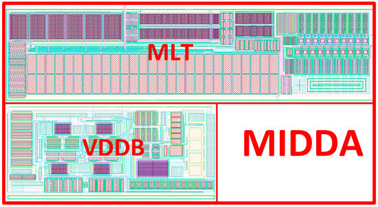
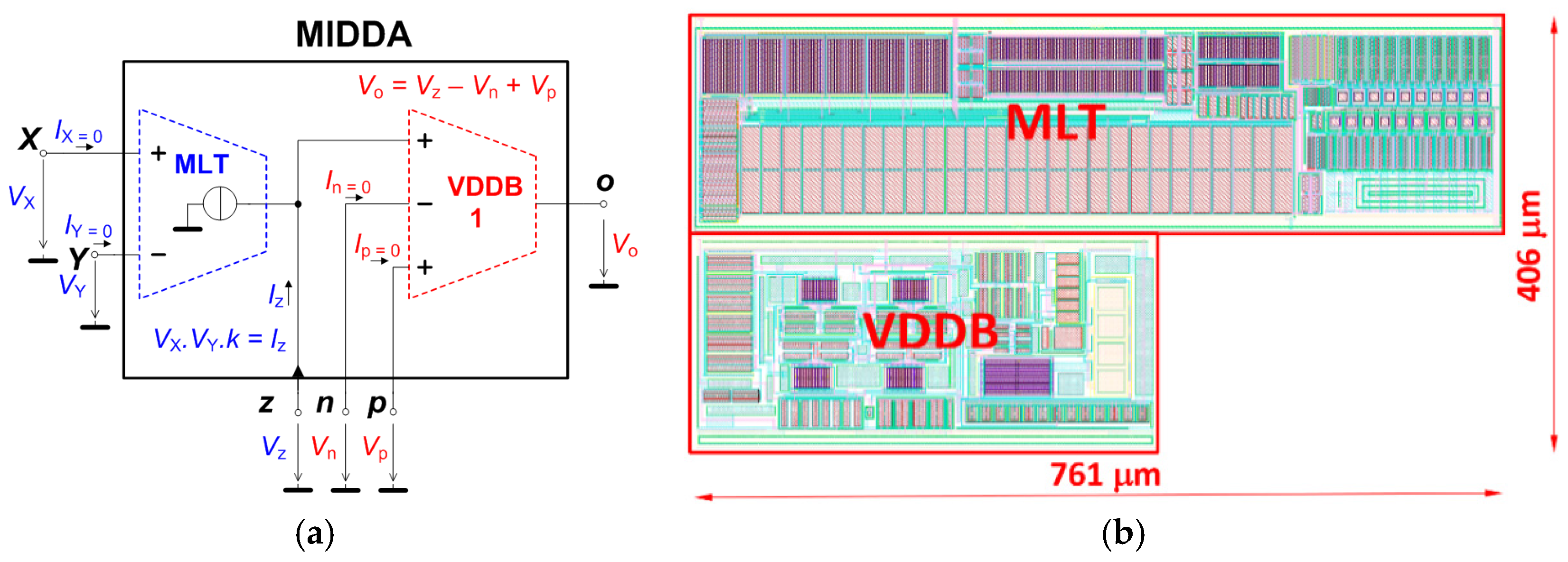
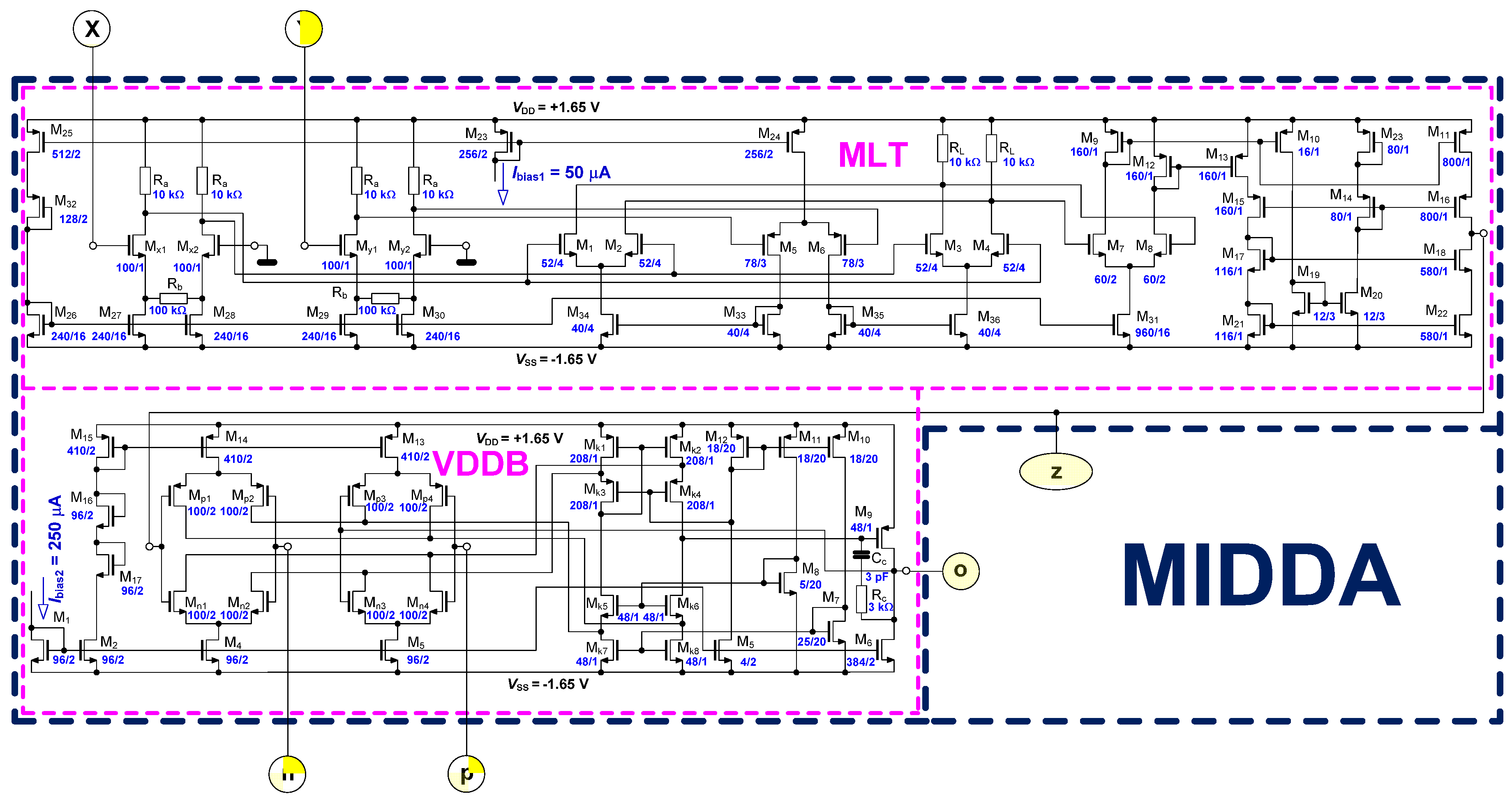
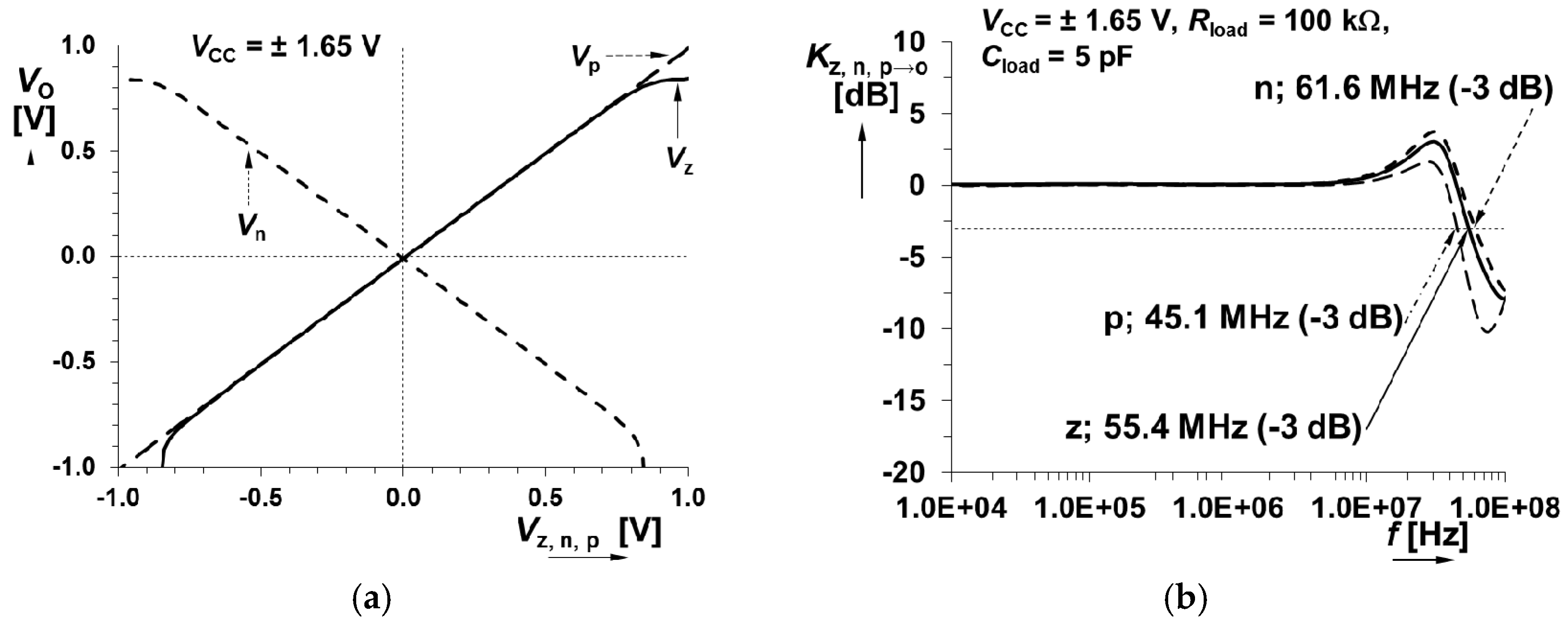
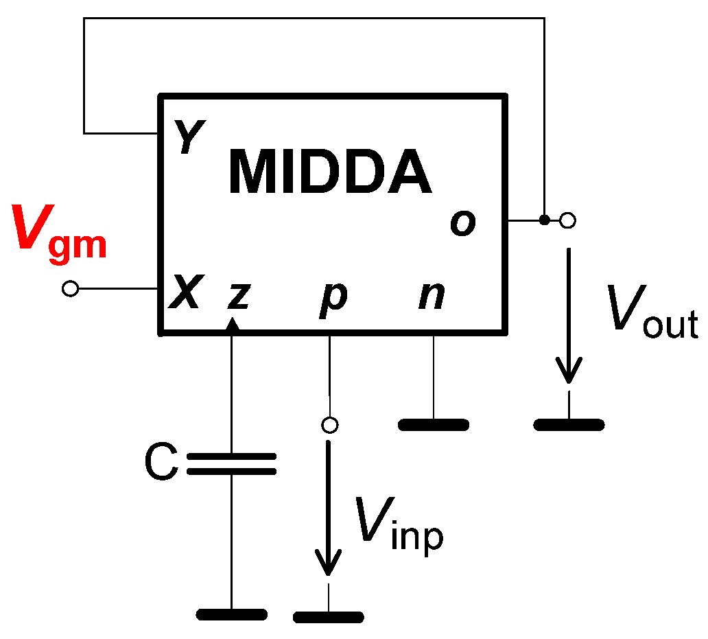
2. A Multiplied Input Differential Difference Amplifier
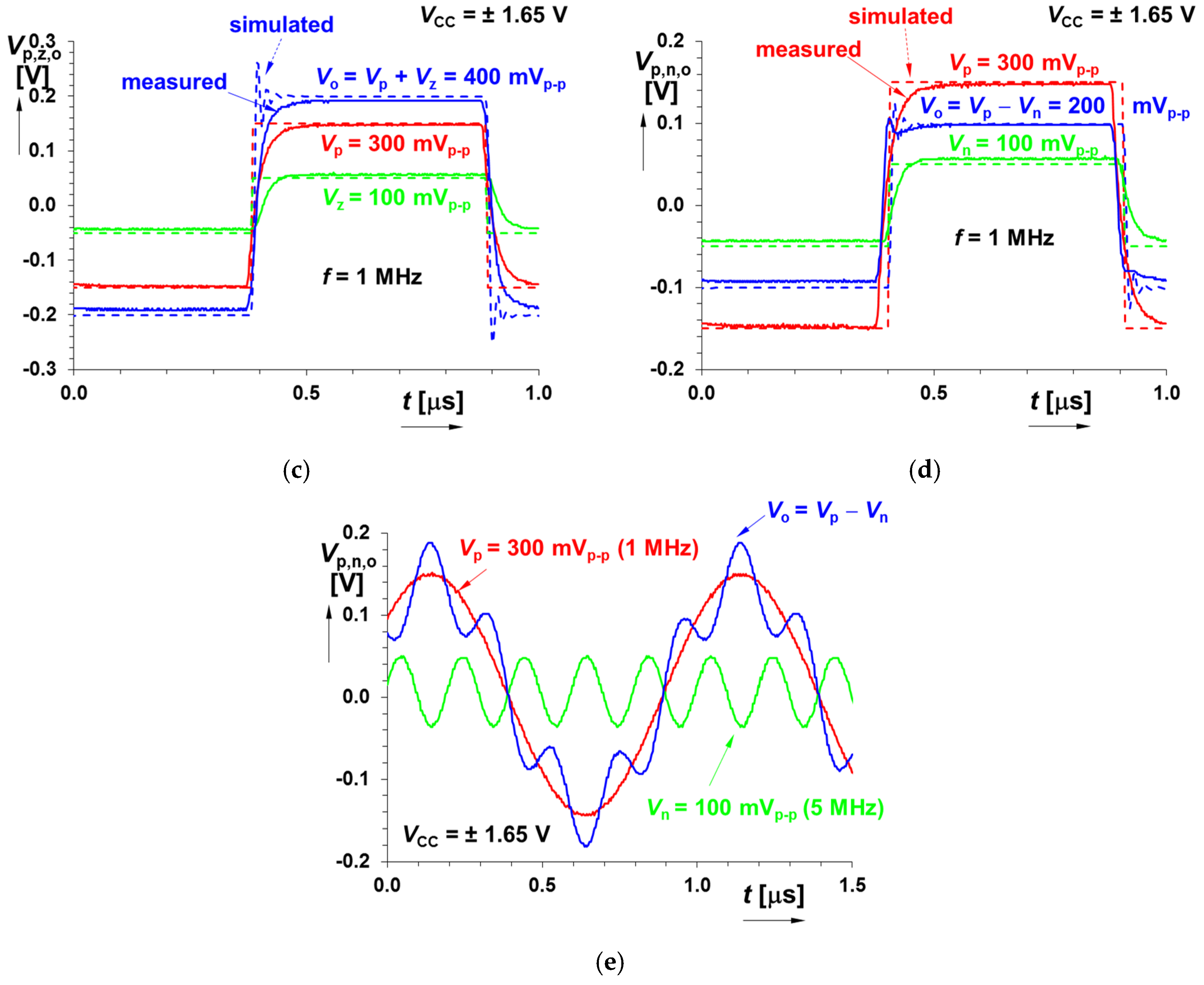
3. Application Examples
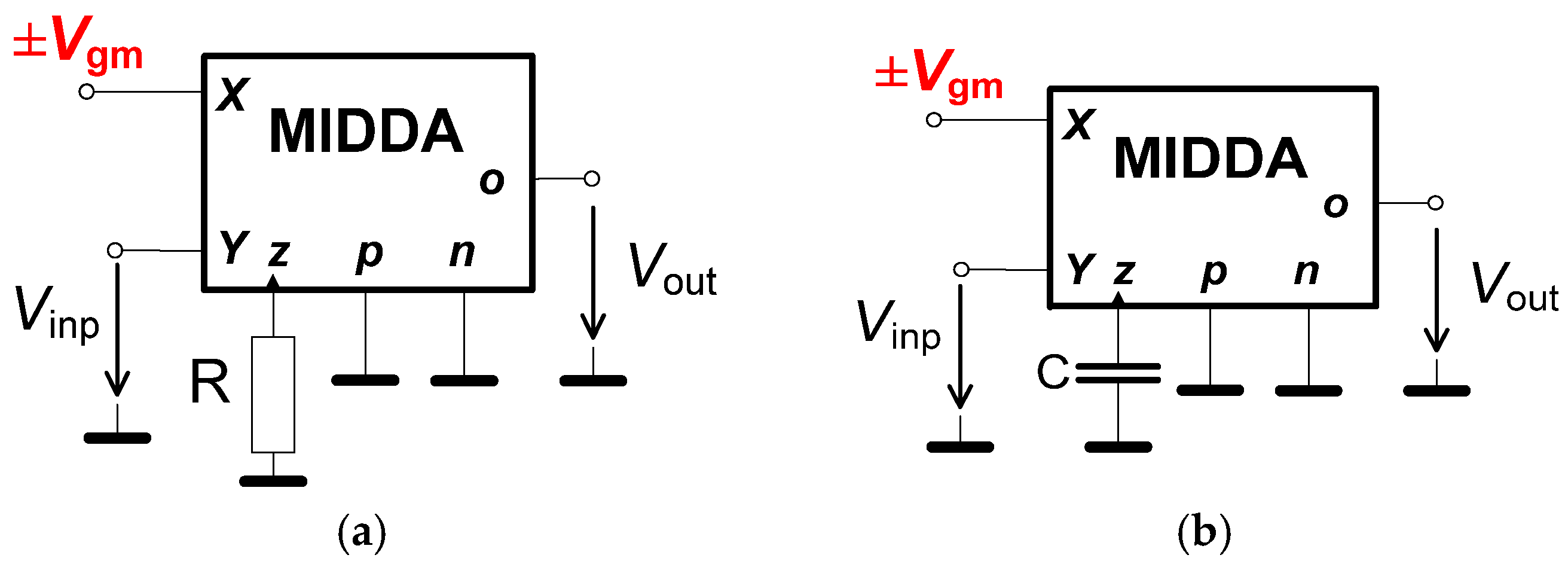
3.1. Simple Linear Applications (Linear Operation)
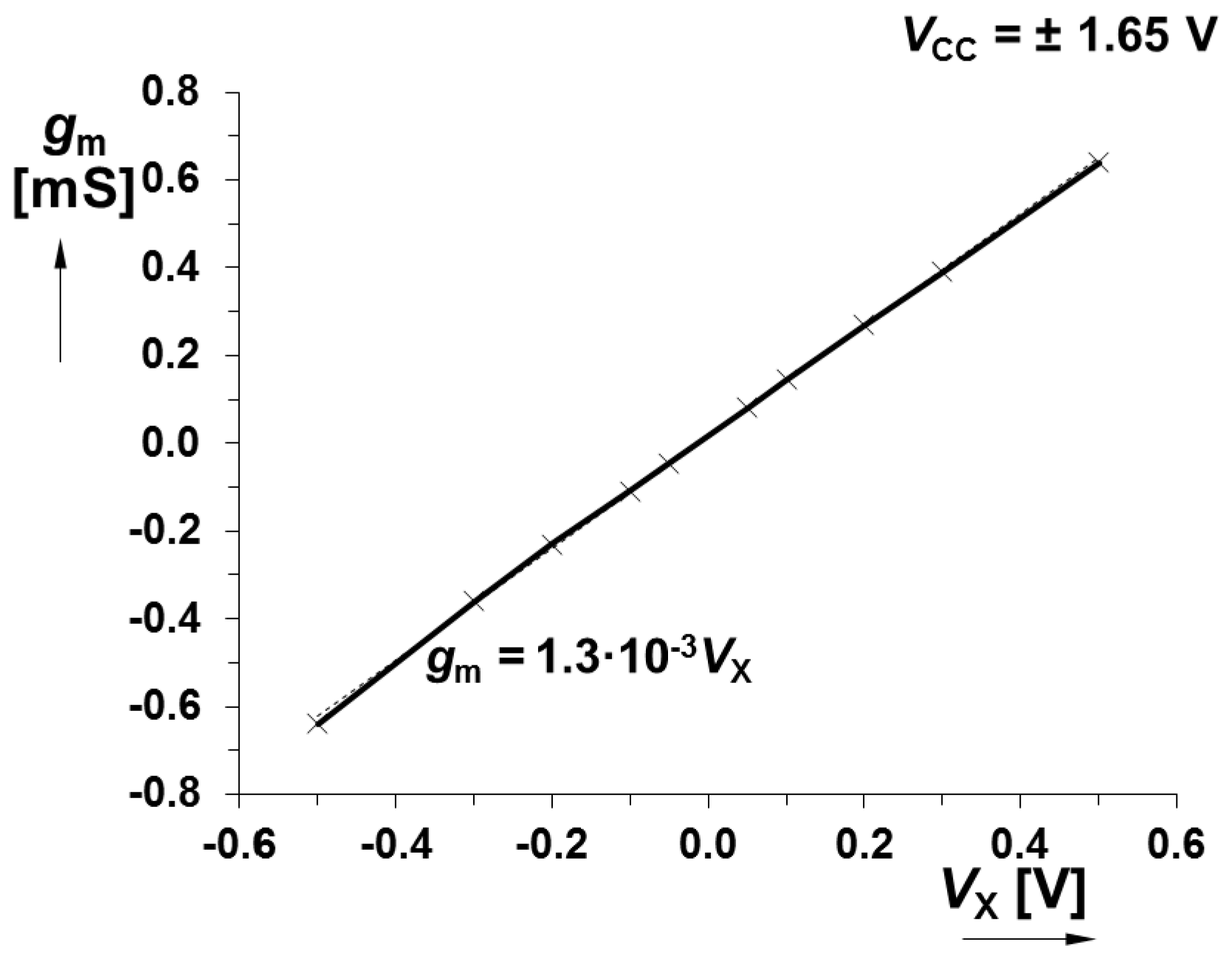
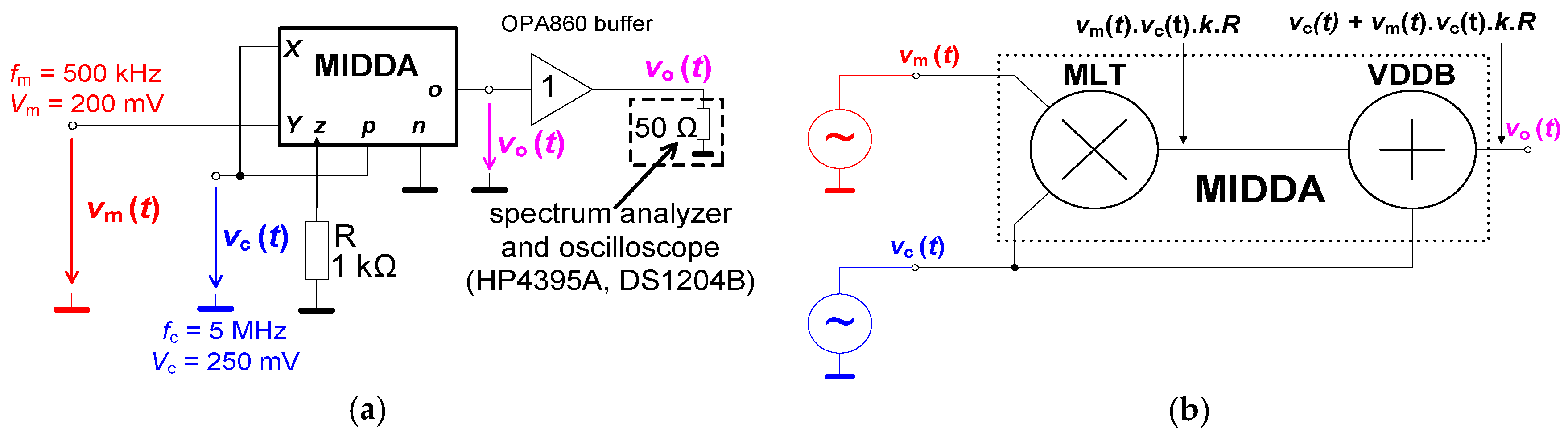
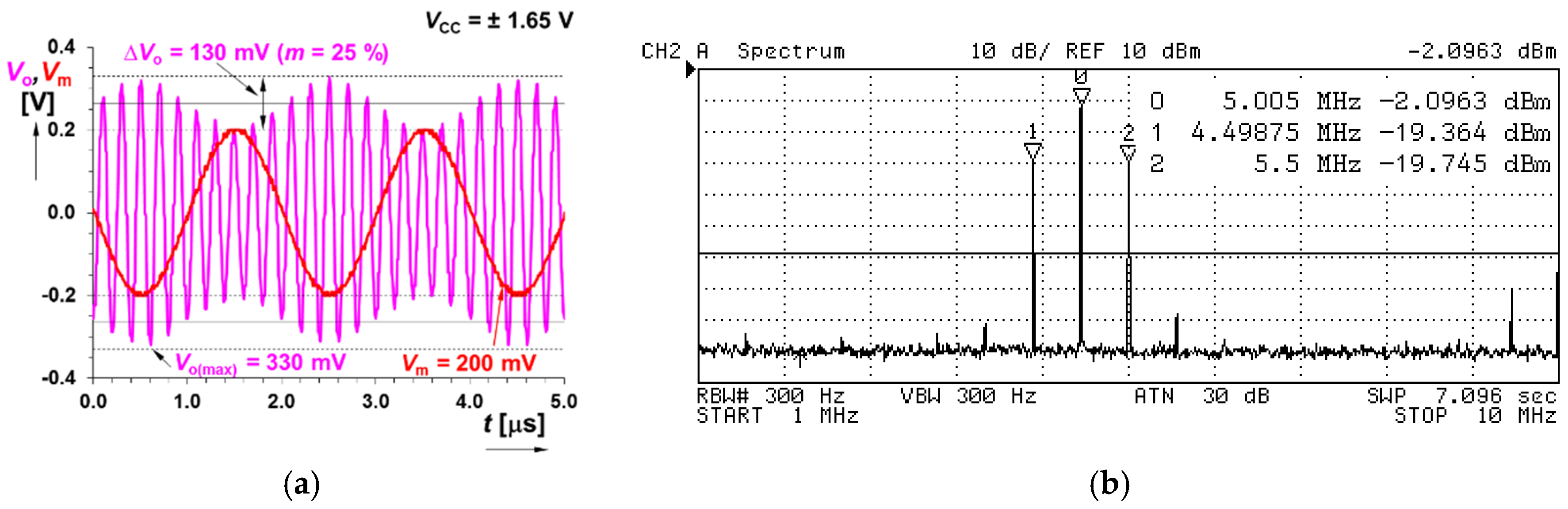
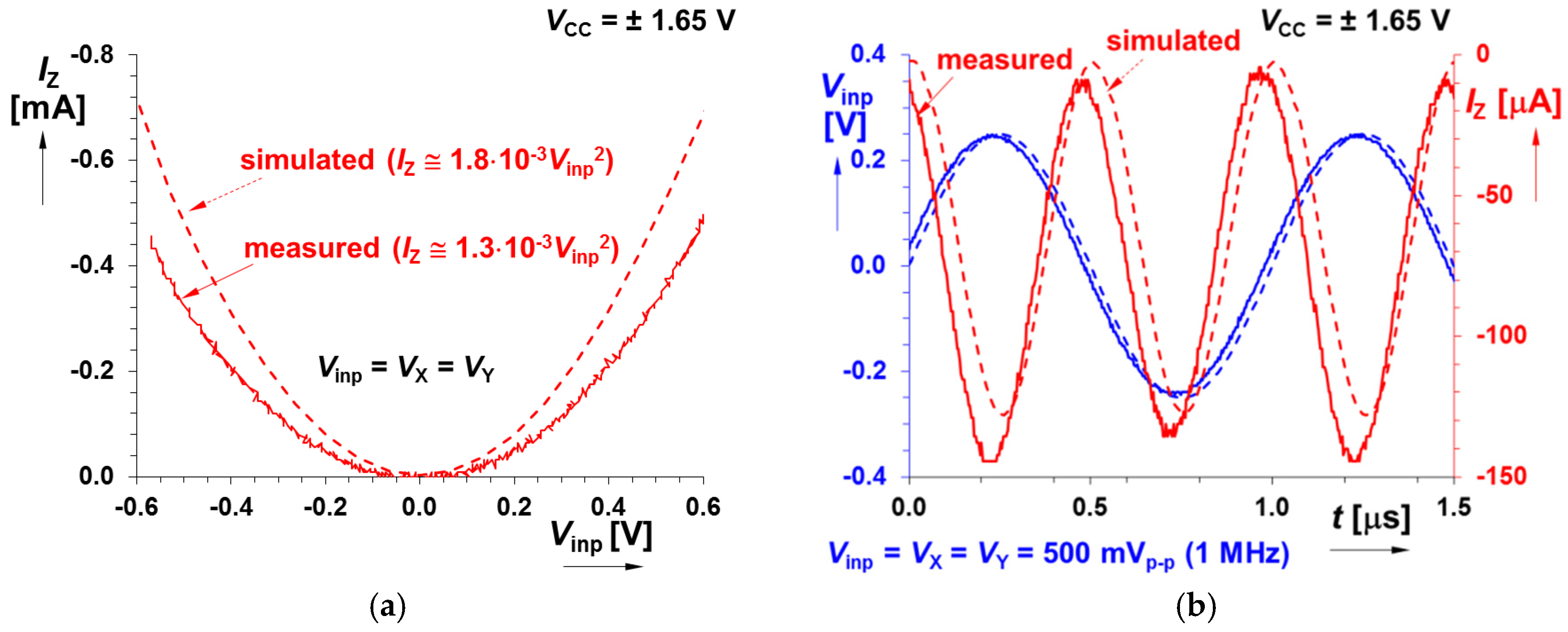
3.2. Simple Nonlinear Application (Nonlinear Operation)
4. Discussion
5. Conclusions
Acknowledgments
Author Contributions
Conflicts of Interest
References
- Biolek, D.; Senani, R.; Biolkova, V.; Kolka, Z. Active elements for analog signal processing: Classification, review, and new proposals. Radioengineering 2008, 17, 15–32. [Google Scholar]
- Senani, R.; Bhaskar, D.R.; Singh, A.K. Current Conveyors: Variants, Applications and Hardware Implementations, 1st ed.; Springer: Berlin/Heidelberg, Germany, 2015. [Google Scholar]
- Biolek, D.; Biolkova, V. Allpass filter employing one grounded capacitor and one active element. Electron. Lett. 2009, 45, 807–808. [Google Scholar] [CrossRef]
- Sotner, R.; Jerabek, J.; Prokop, R.; Kledrowetz, V. Simple CMOS voltage differencing current conveyor-based electronically tuneable quadrature oscillator. Electron. Lett. 2016, 52, 1016–1018. [Google Scholar] [CrossRef]
- Hwang, Y.S.; Liu, W.H.; Tu, S.H.; Chen, J.J. New building block: Multiplication-mode current conveyor. IET Circ. Dev. Syst. 2009, 3, 41–48. [Google Scholar] [CrossRef]
- Venkateswaran, P.; Nandi, R.; Das, S. New integrators and differentiators using MMCC. Circ. Syst. 2012, 3, 288–294. [Google Scholar] [CrossRef]
- Herencsar, N.; Sotner, R.; Metin, B.; Koton, J.; Vrba, K. New ‘Voltage Differencing’ Device for Analog Signal Processing. In Proceedings of the 8th International Conference on Electrical and Electronics Engineering (ELECO), Bursa, Turkey, 28–30 November 2013; pp. 17–20.
- Koton, J.; Herencsar, N.; Vrba, K.; Metin, B. Voltage-mode multifunction filter with mutually independent Q and w0 control feature using VDDDAs. Analog Integr. Circ. Signal Process. 2014, 81, 53–60. [Google Scholar] [CrossRef]
- Jasielsky, J.; Kuta, S.; Machowski, W.; Kolodziejski, W. Four-quadrant CMOS transconductance multiplier operating at low voltage and high-speed. In Proceedings of the 17th International Conference on Mixed Design of Integrated Circuits and Systems (MIXDES), Wroclav, Poland, 14–26 June 2010; pp. 265–268.
- Biolek, D. CDTA-building block for current-mode analog signal processing. In Proceedings of the European Conference on Circuit Theory and Design (ECCTD), Krakow, Poland, 1–4 September 2003; pp. 397–400.
- Rai, S.-K.; Gupta, M. Current differencing transconductance amplifier (CDTA) with enhanced performance and its application. Analog Integr. Circ. Signal Process. 2016, 86, 307–319. [Google Scholar] [CrossRef]
- Jaikla, W.; Siripruchyanun, M.; Bajer, J.; Biolek, D. A Simple Current-Mode Quadrature Oscillator Using Single CDTA. Radioengineering 2008, 17, 33–40. [Google Scholar]
- Siripruchyanun, M.; Jaikla, W. CMOS current-controlled current differencing transconductance amplifier and applications to analog signal processing. AEU Int. J. Electron. Commun. 2008, 62, 277–287. [Google Scholar] [CrossRef]
- Li, Y. Current-mode sixth-order elliptic band-pass filter using MCDTAs. Radioengineering 2011, 20, 645–649. [Google Scholar]
- Prokop, R.; Musil, V. Modular approach to design of modern circuit blocks for current signal processing and new device CCTA. In Proceedings of the 7th International Conference on Signal and Image Processing (IASTED), Anaheim, CA, USA, 15–17 August 2005; pp. 494–499.
- Prokop, R.; Musil, V. New modular current devices for true current mode signal processing. Electronics 2007, 16, 36–42. [Google Scholar]
- Siripruchyanun, M.; Jaikla, W. Current controlled current conveyor transconductance amplifier (CCCCTA): A building block for analog signal processing. Electron. Eng. 2008, 90, 443–453. [Google Scholar] [CrossRef]
- Herencsar, N.; Koton, J.; Vrba, K. Realisation of current mode KHN equivalent biquad using current follower amplifiers (CFTAs). IEICE Trans. Fund. Electron. Commun. Comput. Sci. 2010, E93-A, 1816–1819. [Google Scholar] [CrossRef]
- Singh, B.; Singh, A.K.; Senani, R. New Universal Current-mode Biquad Using Only Three ZC-CFTAs. Radioengineering 2012, 21, 273–280. [Google Scholar]
- Sotner, R.; Herencsar, N.; Jerabek, J.; Prokop, R.; Kartci, A.; Dostal, T.; Vrba, K. Z-Copy Controlled-Gain Voltage Differencing Current Conveyor: Advanced Possibilities in Direct Electronic Control of First-Order Filter. Elektron. Elektrotech. 2014, 20, 77–83. [Google Scholar] [CrossRef]
- Sotner, R.; Jerabek, J.; Herencsar, N. Voltage Differencing Buffered/ Inverted Amplifiers and Their Applications for Signal Generation. Radioengineering 2013, 22, 490–504. [Google Scholar]
- Sotner, R.; Jerabek, J.; Herencsar, N.; Zak, T.; Jaikla, W.; Vrba, K. Modified Current Differencing Unit and its Application for Electronically Reconfigurable Simple First-order Transfer Function. Adv. Electron. Comput. Eng. 2015, 15, 3–10. [Google Scholar] [CrossRef]
- Sotner, R.; Jerabek, J.; Herencsar, N.; Prokop, R.; Lahiri, A.; Dostal, T.; Vrba, K. First-order transfer sections with reconnection-less electronically reconfigurable high-pass, all-pass and direct transfer character. J. Electron. Eng. 2016, 67, 12–20. [Google Scholar] [CrossRef]
- Wang, H.-Y.; Tran, H.-D.; Nguyen, Q.-M.; Yin, L.-T.; Liu, C.-Y. Derivation of Oscillators from Biquadratic Band Pass Filters Using Circuit Transformations. Appl. Sci. 2014, 4, 482–492. [Google Scholar] [CrossRef]


| CMOS MLT Subpart | |
|---|---|
| Parameter/Transfer from→to | |
| Small-Signal AC Transfer (GBW > 42 MHz) | |
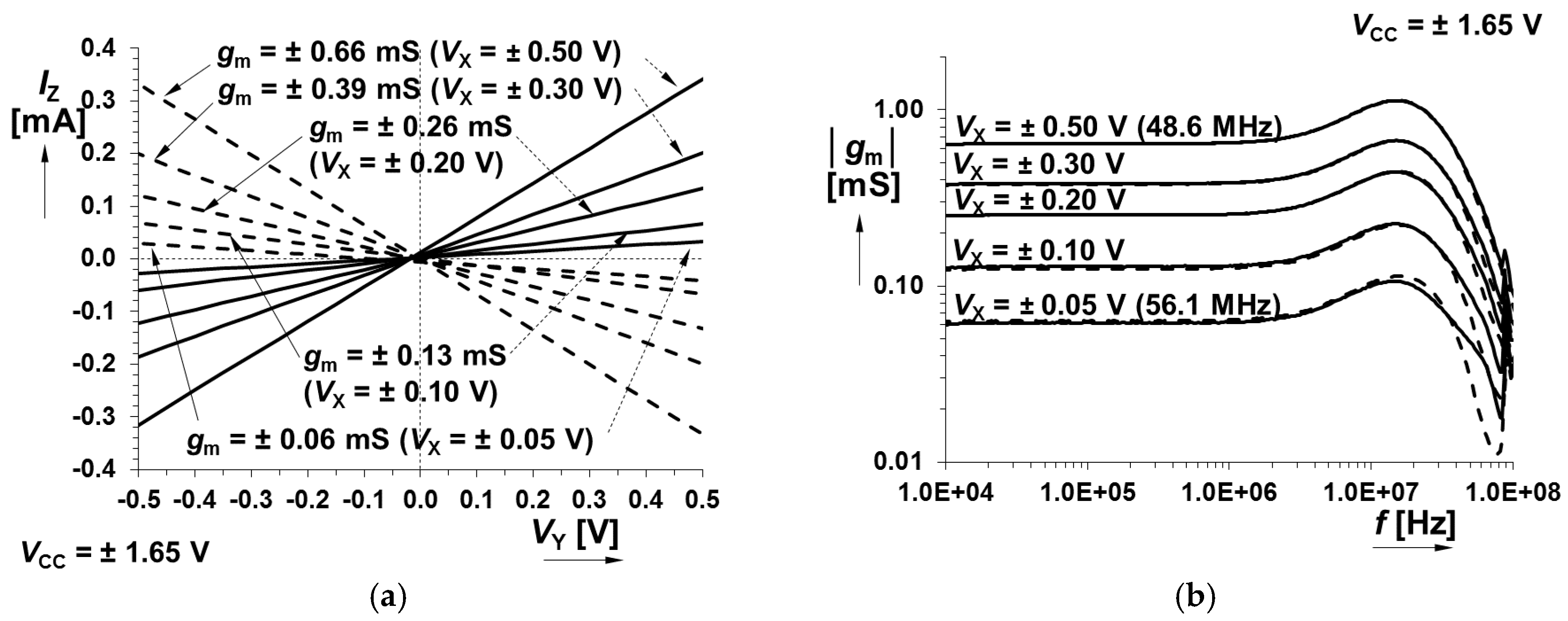
| gm (X→z) (VY = 50→800 mV) | 45→974 μS |
| gm (X→z) (VY = −50→−800 mV) | −80→−2210 μS |
| gm (Y→z) (VX = 50→800 mV) | 60→1030 μS |
| gm (Y→z) (VX = −50→−800 mV) | −62→−1700 μS |
| input DC dynamical range | |
| X→z (VY = ±50→±500 mV) | −500→900 mV |
| Y→z (VX = ±50→±500 mV) | −600→900 mV |
| harmonic distortion | |
| THDX→z (1 kHz, VY = ±1000 mV) | 0.06%→1.08% (for VX = 200→1000 mVpk-pk) |
| THDY→z (1 kHz, VX = ±1000 mV) | 0.08%→1.38% (for VY = 200→700 mVpk-pk) |
| input/output resistances | |
| RX_DC (any value of VY) | 100 MΩ |
| RY_DC (any value of VX) | 100 MΩ |
| Rz_DC (VY = 50→800 mV) | 1 MΩ→176 kΩ |
| Rz_DC (VY = −50→−800 mV) | 3 MΩ→140 kΩ |
| Rz_DC (VX = 50→800 mV) | 66 kΩ→5.2 kΩ |
| Rz_DC (VX = −50→−800 mV) | 107 kΩ→2.4 kΩ |
| CMOS VDDB Subpart | |
| small-signal AC transfer | |
| Kz→O [−] (−3 dB) | 1.02 (55 MHz) |
| Kn→O [−] (−3 dB) | 1.02 (62 MHz) |
| Kp→O [−] (−3 dB) | 1.01 (45 MHz) |
| input dynamical range | |
| z→o | −800→700 mV |
| n→o | −700→700 mV |
| p→o | −1600→1000 mV |
| distortion | |
| THDz→o | 0.04%→0.41% (for Vz = 100→1500 mVpk-pk) |
| THDn→o | 0.07%→0.33% (for Vn = 100→1500 mVpk-pk) |
| THDp→o | 0.03%→0.11% (for Vp = 100→1500 mVpk-pk) |
| input/output resistances | |
| Rz,n,p | 100 MΩ |
| RO | 0.54 Ω |
| Work | Active Device | No. of Terminals f | No. of Controllable Parameters (Type) | MULTIPLICATIVE Inter-Terminal Relation Available | Device Fabricated as IC |
|---|---|---|---|---|---|
| [1,3,10,11,12] | CDTA 1 | 5 | 1 (gm) a | No | Yes |
| [13] | CCCDTA 2 | 4 | 3 (Rp, Rn, gm) b | No | No |
| [14] | MCDTA 3 | 8 | 2 (gm1, gm2) | No | No |
| [15,16] | CCTA 4 | 4 | 1 (gm) | No | Yes |
| [17] | CCCCTA 5 | 4 | 2 (RX, gm) | No | No |
| [18,19] | CFTA, ZC-CFTA 6 | 4 (5) | 1 (gm) | No | No |
| [4,20] | VDCC, ZC-CG-VDCC 7 | 6 (7) | 2 (RX, gm) 3 (RX, gm, B) c | No | Yes |
| [21] | DO-VDBA 8 | 5 | 1 (gm) | No | No |
| FB-VDBA 9 | 6 | 1 (gm) | |||
| DO-CG-VDBVA 10 | 6 | 2 (gm, A) d | |||
| [22] | MCDU 11 | 5 | 4 (Rp, Rn, B1, B2) | No | No |
| [23] | ZC-CCCFDITA 12 | 6 | 2 (Rf, gm) | No | No |
| [7,8] | VDDDA 13 | 6 | 1 (gm) | No | No |
| [5,6] | MMCC 14 | 4 | 1 (A) e | Yes | No |
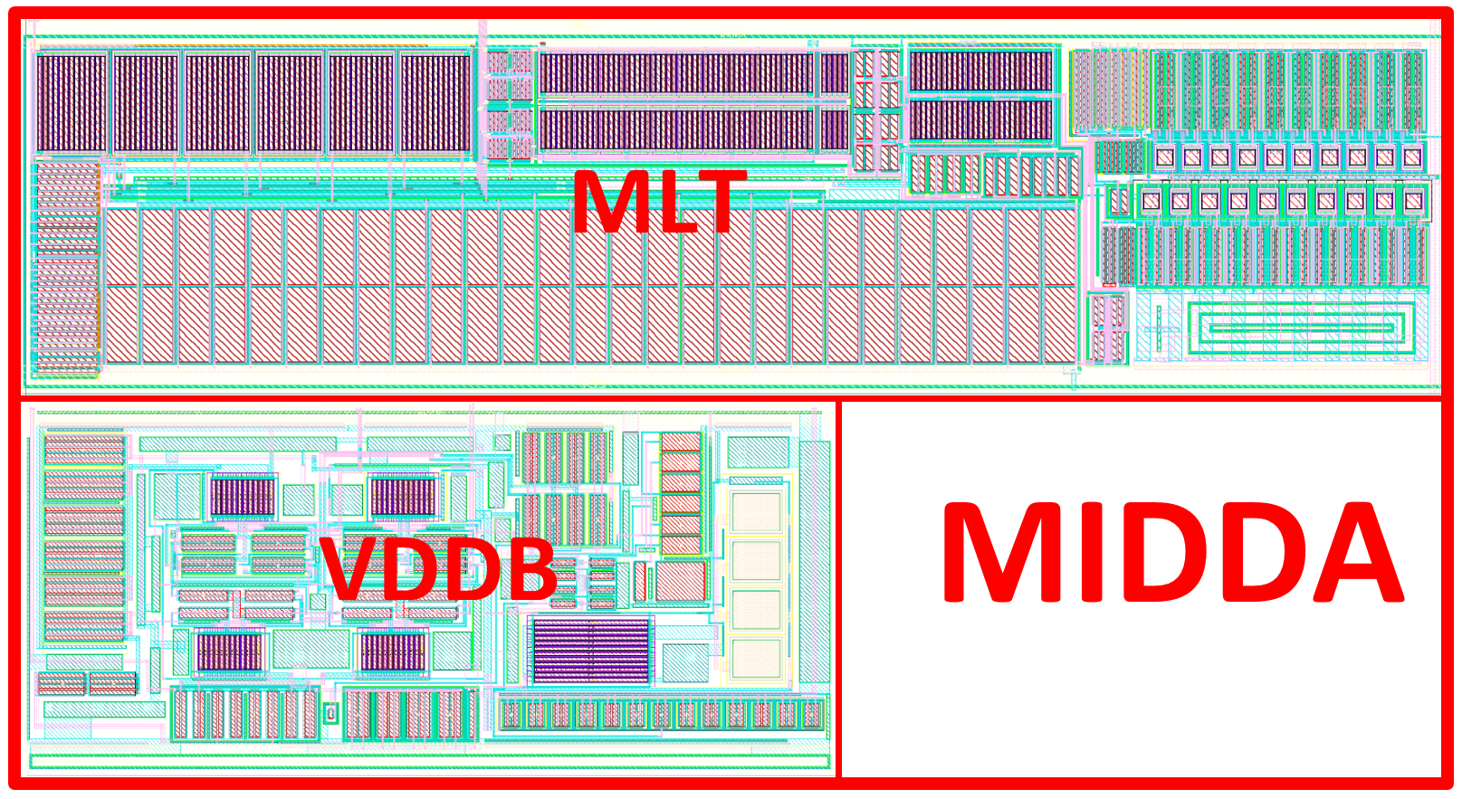
| this work | MIDDA | 6 | 1 (gm) e | Yes | Yes |
© 2017 by the authors; licensee MDPI, Basel, Switzerland. This article is an open access article distributed under the terms and conditions of the Creative Commons Attribution (CC BY) license (http://creativecommons.org/licenses/by/4.0/).
Share and Cite
Sotner, R.; Jerabek, J.; Prokop, R.; Kledrowetz, V.; Polak, J. A CMOS Multiplied Input Differential Difference Amplifier: A New Active Device and Its Applications. Appl. Sci. 2017, 7, 106. https://doi.org/10.3390/app7010106
Sotner R, Jerabek J, Prokop R, Kledrowetz V, Polak J. A CMOS Multiplied Input Differential Difference Amplifier: A New Active Device and Its Applications. Applied Sciences. 2017; 7(1):106. https://doi.org/10.3390/app7010106
Chicago/Turabian StyleSotner, Roman, Jan Jerabek, Roman Prokop, Vilem Kledrowetz, and Josef Polak. 2017. "A CMOS Multiplied Input Differential Difference Amplifier: A New Active Device and Its Applications" Applied Sciences 7, no. 1: 106. https://doi.org/10.3390/app7010106
APA StyleSotner, R., Jerabek, J., Prokop, R., Kledrowetz, V., & Polak, J. (2017). A CMOS Multiplied Input Differential Difference Amplifier: A New Active Device and Its Applications. Applied Sciences, 7(1), 106. https://doi.org/10.3390/app7010106