Abstract
In this paper, a detailed and systematic derivation of the output filter in a novel dual-input photovoltaic (PV)-wind converter (DIPWC) is presented. The theoretical derivation is based on an energy balance principle. While the DIPWC operates in steady state, the amount of charged energy of the output filter will be equal to that of the energy pumped away within one switching cycle. From this zero net change in energy, the minimum value of the output filter can be found. With the determined value, the DIPWC is able to operate in continuous conduction for high power applications. The developed procedure of the inductance determination can be applied to other types of dual-input converters. Therefore, it makes significant contributions to the design toward a green-energy, multi-input converter. To verify the correctness of the mathematical analysis, the DIPWC—with the derived output inductance—is built and tested. Practical measurements and results have verified the inductance determination.
1. Introduction
Nowadays, renewable energies, such as photovoltaic (PV), wind energy and hydroelectric, have been widely adopted as alternatives to fossil fuels. However, output power of a renewable-energy generator is highly affected by atmospheric conditions. Therefore, a hybrid power system—including two or more input sources—has become the design trend for renewable energy processing, in which a constant output voltage and sustained power supply can be completed [,,,,,].
A dual-input converter (DIC) can simultaneously deal with two inputs and obtains a regulated voltage [,,,,,]. For renewable power applications, a DIC should have the ability to process renewable energy for each individual input. Even though neither of the inputs has the power to feed, the DIC can still function well. In addition, the DC-bus voltage of a grid-connected system is normally up to 380 V. That is, the DIC must be capable of achieving a high step-up feature [,,,,,,,,]. In order to meet the marketable requirements, a DIC should have the features of high efficiency, cost-effectiveness, a low electromagnetic interference (EMI), small size, minimum component counts, and a low current ripple. In [,], an isolated DIC with multi-windings, based on the flux additivity concept, is proposed to accomplish some of the mentioned features. However, each power MOSFET in the DIC has to be in series with a reverse-blocking diode, which results in the energy stored in the leakage inductors not being recycled and causes a high voltage spike on MOSFET during turn-on and turn-off transitions. Adopting a clamp circuit or snubber may be an approach to alleviate the mentioned voltage spike and to reduce power loss []. Nevertheless, this approach increases the power component count and cannot improve the voltage conversion ratio.
In this paper, a novel power DIC is presented, which can process PV power and wind-turbine energy simultaneously or individually and its so called novel dual-input PV-wind converter (DIPWC). For continuous current operation and output voltage regulation, the output port adopts a second-order LC filter in cascade connection to the converter. The inductance of the output filter will dominate the feature of the DIPWC. However, the determination of the inductance has a sophisticated procedure. Therefore, this paper will first describe the operation of the DIPWC and then design the inductance theoretically.
Following the introduction in Section 1, the remainder of this paper is organized as follows. Section 2 briefly introduces the characteristics of the proposed DIPWC. The circuit operation principle of the converter and control mechanism are discussed in Section 3. A theoretical analysis for determining an optimal value of the output inductor is presented in Section 4. To verify the correctness of the theoretical analysis, a DIPWC prototype with the designed filter is built. Key experimental results will be illustrated in Section 5. Finally, Section 6 summarizes the conclusions.
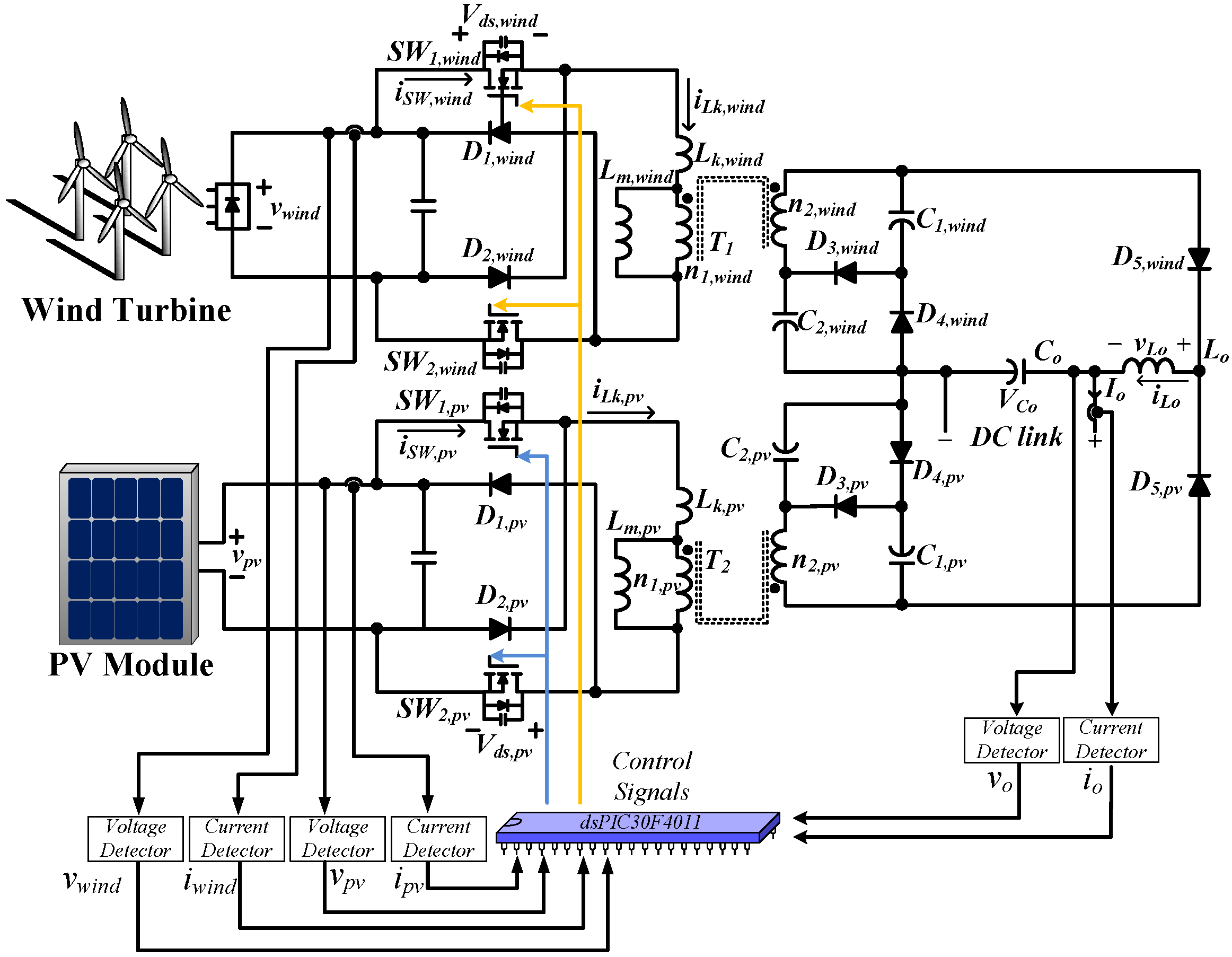
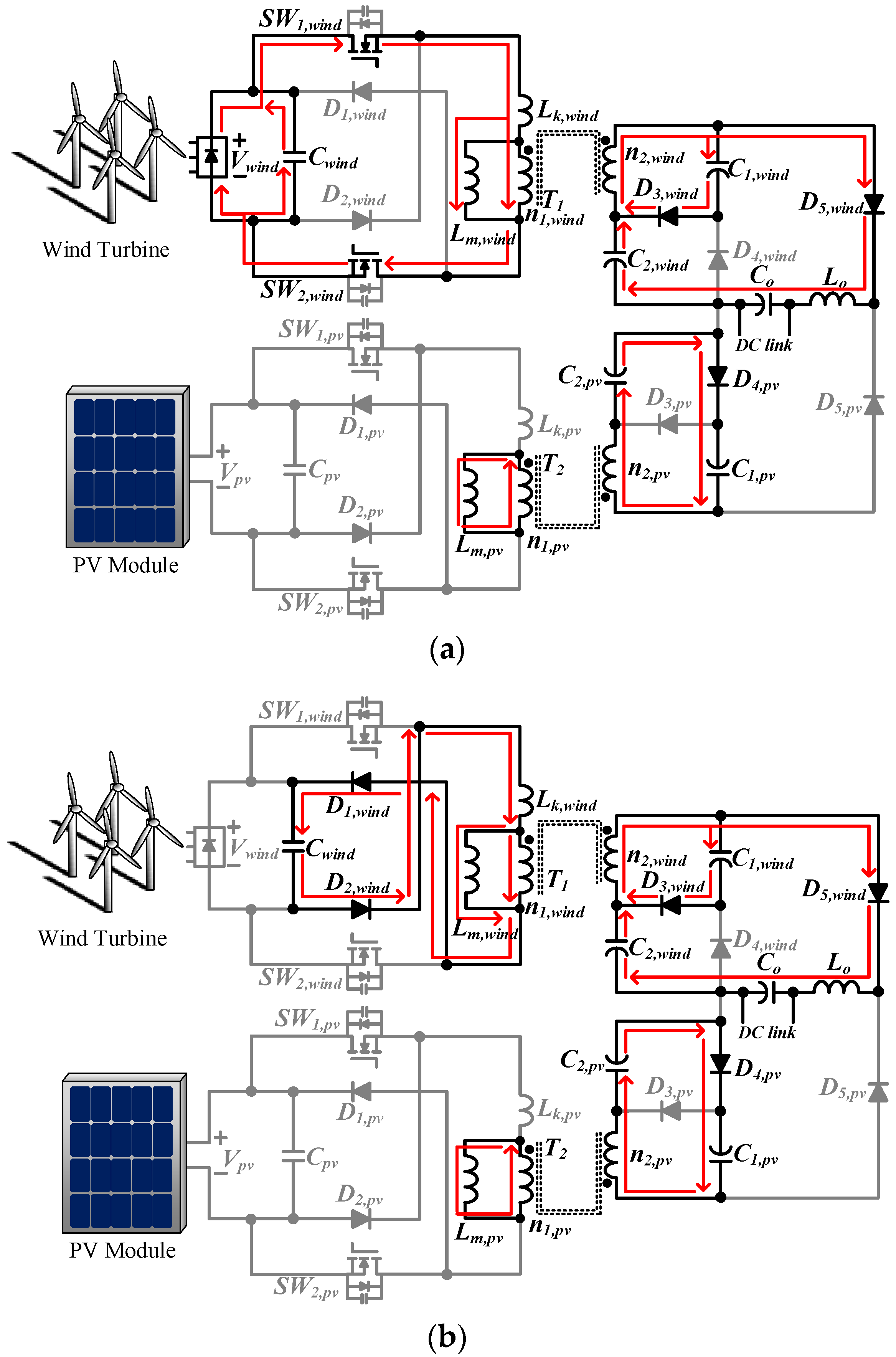
2. Characteristics of Proposed Converter
Figure 1 shows the circuit configuration of the proposed DIPWC in this paper, which mainly consists of two coupled inductors, four power MOSFETs, four capacitors, ten diodes, and an LC filter. The proposed DIPWC can conceptually be regarded as the integrating of two double-ended forwards with voltage multipliers. This structure can recycle the energy stored in the leakage inductors, Lk,wind and Lk,pv, to their corresponding power inputs. By controlling the appropriate power switches with pulse-width modulation (PWM), the DIPWC can draw renewable energy and then feed power to the DC bus. The input renewable energy can come from either a PV panel, a wind turbine or both. During a switch cycle, when all the switches are in an off state, the output inductor Lo has to release energy to the DC bus to continually provide power. A renewable generation system—to deal with the high power rating—will accompany a high level of output current. As a result, the DIPWC should operate in continuous conduction mode (CCM) to lower current stresses of semiconductor devices. This reason has revealed the importance of the design relating to output-filter inductance.
Figure 1.
The configuration of the presented dual-input photovoltaic-wind converter (DIPWC).
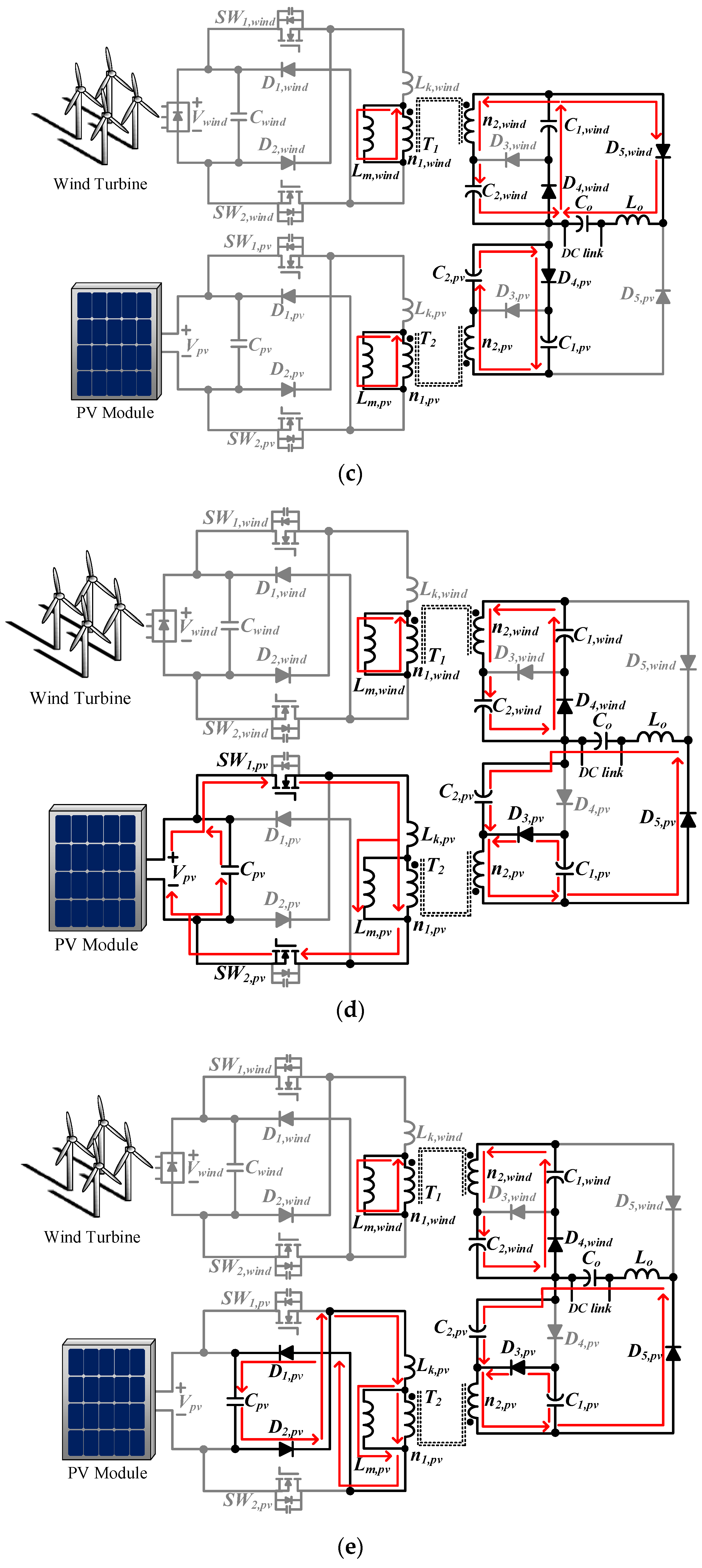
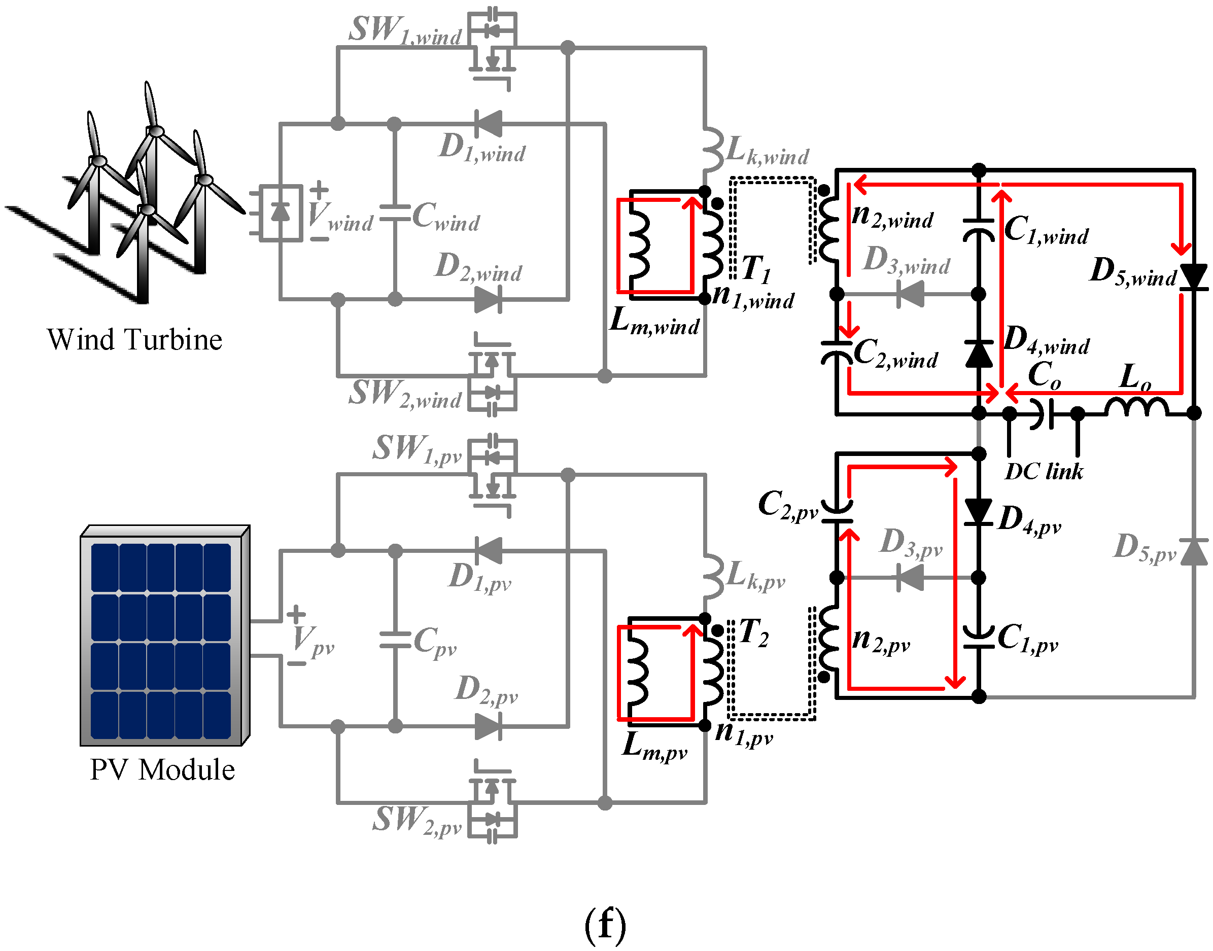
3. Operation Principle
The operation of the DIPWC can be divided into six stages. Figure 2 shows the related equivalents, while corresponding key waveforms are depicted in Figure 3. In Figure 1, the magnetizing inductances, Lm,wind and Lm,pv, are both in CCM. To simplify the circuit analysis, there are some assumptions made in the following.


Figure 2.
Equivalent circuits of the DIPWC: (a) Stage 1, (b) Stage 2, (c) Stage 3, (d) Stage 4, (e) Stage 5, and (f) Stage 6.
Figure 3.
Conceptual key waveforms of the DIPWC.
- (1)
- In Figure 2, capacitances of C1,wind, C2,wind, C1,pv, and C2,pv are large enough so that all the voltages across them can be regarded as constant in a switching cycle.
- (2)
- The internal resistances and parasitic capacitances in all active switches are neglected.
- (3)
- All diodes are ideal.
Stage 1 [t0, t1]: Refer to Figure 2a for Stage 1. Switches SW1,wind and SW2,wind are closed, whereas SW1,pv and SW1,pv are opened. The wind-turbine input voltage Vwind forward energy to Lm,wind via the loop of Vwind-SW1,wind-Lk,wind-Lm,wind-SW2,wind. Meanwhile, the output inductor Lo and capacitor Co absorb energy from C2,wind, so that the current flowing through Lo, iLo, increases linearly. The capacitor C2,pv is charged by the magnetizing inductor Lm,pv. This stage ends as the SW1,wind and SW2,wind are turned off.
Stage 2 [t1, t2]: The equivalent of Stage is shown in Figure 2b. During this time interval, all the switches are open. The leakage inductor Lk,wind dumps energy to capacitor Cwind via the loop of Lk,wind-D1,wind-Cwind-D2,wind. The current of the leakage inductor Lk,wind, iLk,wind, decreases rapidly. At output, the Lo powers output and its current decreases accordingly. This stage ends when the current iLk,wind falls to 0.
Stage 3 [t2, t3]: Figure 2c depicts the equivalent circuit of this stage, in which all the switches are open. Magnetizing inductors, Lm,wind and Lm,pv, release their energy to C2,wind and C2,PV , respectively. The capacitor C1,wind charges Co by the loop of Co-D4,wind-C1,wind-D5,wind-Lo. The operation of the converter enters into the next stage when SW1,pv and SW2,pv are simultaneously turned off.
Stage 4 [t3, t4]: This stage begins at t = t4. Figure 2d illustrates the equivalent. In Stage 4, both switches SW1,pv and SW2,pv are closed, whereas SW1,wind and SW1,wind are opened. The PV input voltage Vpv forwards energy to Lm,pv through the loop of Vpv-SW1,pv-Lk,pv-Lm,pv-SW2,pv. The energy stored in the magnetizing inductor Lm,wind is released to the secondary of the coupled inductor T1 to charge C2,wind. The inductor Lo and capacitor Co absorb energy from C2,pv; therefore, the current of Lo, iLo, increases linearly. As the SW1,pv and SW2,pv are turned off again, this stage ends.
Stage 5 [t4, t5]: As referred to in Figure 2e, it can be found that all the switches are in an off state in Stage 5. The leakage inductor Lk,pv charges capacitor Cpv and its current drops steeply. In addition, output inductor Lo pumps energy to Co, which results in a linear decrease at current iLo. At the moment that current iLk,pv drops to 0, Stage 6 begins.
Stage 6 [t5, t6]: Figure 2f shows the equivalent circuit of this stage, in which all the switches are open. Capacitors C2,wind and C2,pv are charged by magnetizing inductors, Lm,wind and Lm,pv, respectively. The output absorbs energy from C1,wind via the loop of Co-D4,wind-C1,wind-D5,wind-Lo. When SW1,wind and SW2,wind are turned on again, this stage ends and the operation of the DIPWC over one switch cycle is completed.
To achieve MPPT, the simplest MPPT algorithm, the perturb-and-observe method, is adopted to reach the maximum power point, as shown in Figure 4. The MPPTs for the wind turbine and PV module are controlled independently. Accordingly, the terminal voltages and currents of the wind turbine and PV module, vwind, iwind, vpv and ipv, have to be detected for the calculation of each input power. Then, based on the truth table and the corresponding flowchart, as shown in Table 1 and Figure 5, respectively, duty ratios of the four active switches are determined for MPPT accomplishment. All the control is completed by a microcontroller dsPIC30F4011, which is illustrated in Figure 1.
Figure 4.
P-V curve of photovoltaic (PV) module.
Table 1.
Truth table of the perturb-and-observe method.
Figure 5.
The flowchart of the perturb-and-observe method.
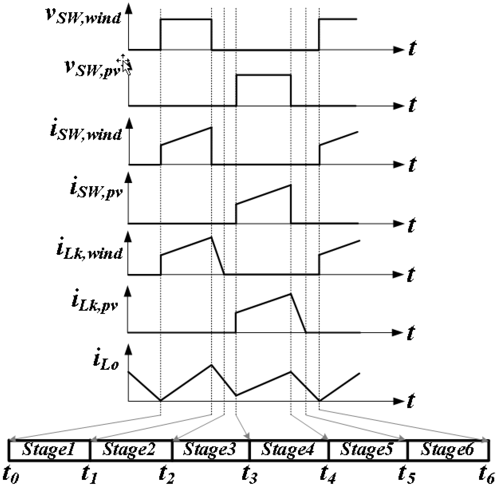
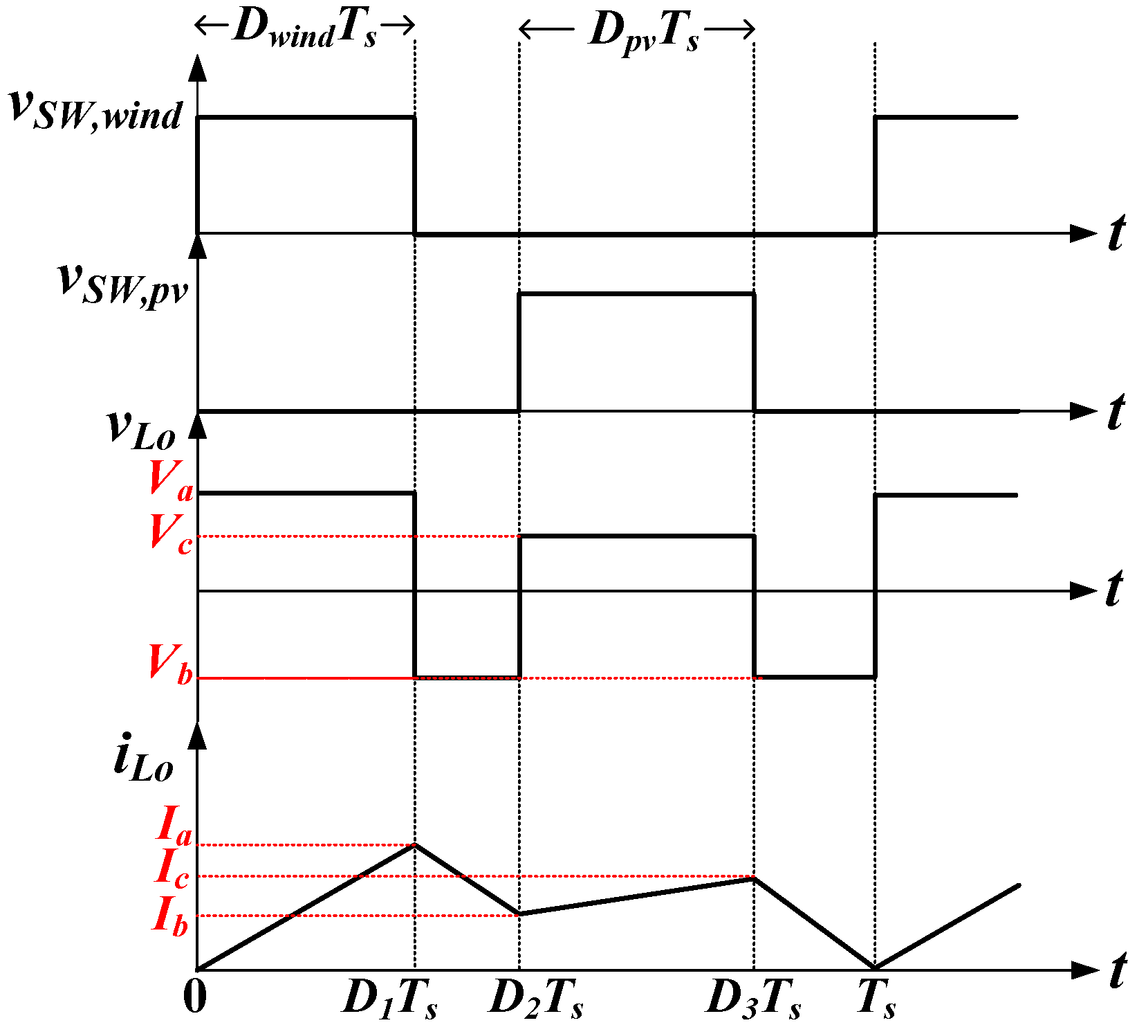
4. Inductance Derivation
Conceptual waveforms of gate signals and output inductor voltage and current are illustrated in Figure 6, in which the switches SW1,wind and SW2,wind are closed for DwindTs and SW1,pv and SW2,pv are closed for DpvTs, respectively. Since the voltage ripple at each capacitor is much less than the average capacitor voltage, the voltage across the output inductor can be regarded as constant under all switch statuses. Accordingly, the current flowing through the output inductor will be piecewise linear over one switching cycle. The derivation of the output inductance of the DIPWC is sophisticated. For a clear description, the related procedure is summarized as follows.
Figure 6.
The waveforms for the understanding of inductance derivation.
- Step 1:
- Find the voltages across C1,wind and C1,pv, VC1,wind and VC1,pv.
- Step 2:
- Apply energy balance principle to Lm,wind and Lm,pv to determine the voltages across C2,wind and C2,pv, respectively.
- Step 3:
- Apply volt-second balance criterion (VSBC) to Lo to determine the output capacitor voltage VCo.
- Step 4:
- After obtaining all capacitor voltages VC1,wind, VC2,wind, VC1,pv, VC2,pv, and VCo, calculate the voltage levels of Lo during the intervals of DwindTs, DpvTs, and (1 − Dwind − Dpv)Ts.
- Step 5:
- Step 6:
- Estimate the average current of Lo, ILo,avg.
- Step 7:
- From the equation of ILo,avg obtained in Step 6, find the minimum inductance of Lo for the CCM operation.
Following the previous seven steps, a detailed derivation of output inductance is presented below. From Figure 2a, it can be observed that the voltage VC1,wind is n times the magnitude of Vwind if the leakage inductor Lk,wind is neglected. That is,
Meanwhile, the current increment on magnetizing inductor Lm,wind can be estimated by
When switches SW1,wind and SW2,wind are both turned off, the voltage polarity of Lm,wind reverses. The energy stored in Lm,wind will be forwarded to the secondary of the coupled inductor T1 to charge the capacitor C2,wind, and then the current iLm,wind decreases. The descent is calculated as:
Based on the energy balance principle, that is, net current change in Lm,wind being zero, the voltage across C2,wind can be expressed as:
Similarly, from Figure 2d, in which the switches SW1,pv and SW2,pv are closed, the voltage VC1,pv and the current increment on the magnetizing inductor Lm,pv can be represented by:
and
respectively. Once SW1,pv and SW2,pv are turned off, the capacitor C2,pv begins absorbing energy from C1,pv, resulting in current decrease in Lm,pv. The current drop is estimated as follows:
In steady state, net current change is zero, which yields:
Subsequently, the finding for VCo is discussed. When the switches SW1,wind and SW2,wind are in the on state, the output inductor Lo will absorb energy from C2,wind via the loop of Co-C2,wind-n2,wind-D5,wind-Lo. Thus, the voltage across Lo over the time interval DwindTs can be given by:
During the interval DpvTs, the switches SW1,pv and SW2,pv are in the on state, which results in the output inductor Lo absorbing energy from C2,pv via the loop of Co-C2,pv-n2,pv-D5,pv-Lo. In this time interval, the voltage across Lo becomes:
As shown in Figure 2c, the statuses of the four switches are open in the remaining time of a switching period, (1 − Dwind − Dpv)Ts. The inductor Lo releases energy and its voltage is valued as:
By applying VSBC to Lo and deriving with Equations (9)–(11), the following relationship holds:
Rearranging equation (12), one can obtain the following representation of VCo:
The values of Va, Vb and Vc shown in Figure 6 can be found by substituting (13) into (9), (10), and (11).
and
Once Va, Vb and Vc have been determined, the inductor currents at the time points, t = D1Ts, D2Ts, and D3Ts, can be readily calculated. The current magnitudes at these time points are Ia, Ib, and Ic, in turn, which are estimated as follows:
and
In Step 6, the average current of iLo, ILo,avg, is the integral over the period Ts. That is,
Calculating and simplifying the equation (20) results:
According to Ampere Second Balance (ASBC), the average current of the output capacitor Co should be zero. As a result, the current ILo,avg is equal to the load current Io. Then, substituting (14), (15), (16), (17), (18), and (19) into (21), one can obtain the minimum inductance of Lo for CCM as follows:
With respect to capacitor design, voltage ripple dominates capacitance determination. Voltage ripple across a capacitor, Δvc, can be found by:
where Δvc stands for charge variation during time interval Δt, ic is the current flowing through the capacitor, and C is the corresponding capacitance. The currents of capacitors C1,wind, C2,wind, C1,pv, C2,pv and Co are iD3,wind, iD4,wind, D3,pv, D4,pv and iLo-Io, respectively. According to the operation principle discussed in Section 3, the voltage ripples across capacitors C1,wind, C2,wind, C1,pv, C2,pv and Co can be estimated as follows:
and
From (24)–(28), the capacitances of C1,wind, C2,wind, C1,pv, C2,pv and Co can be readily computed.
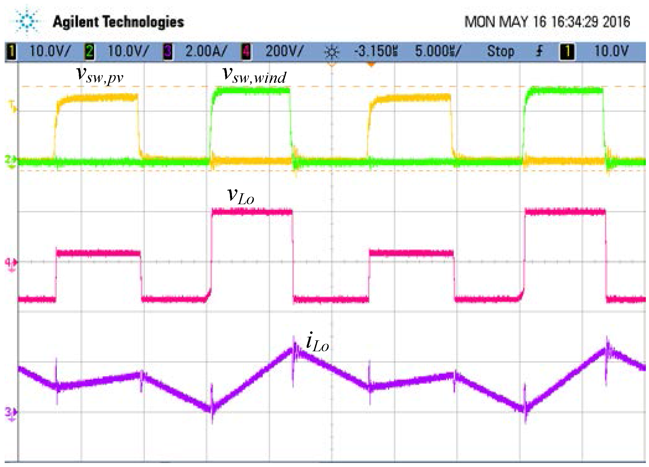
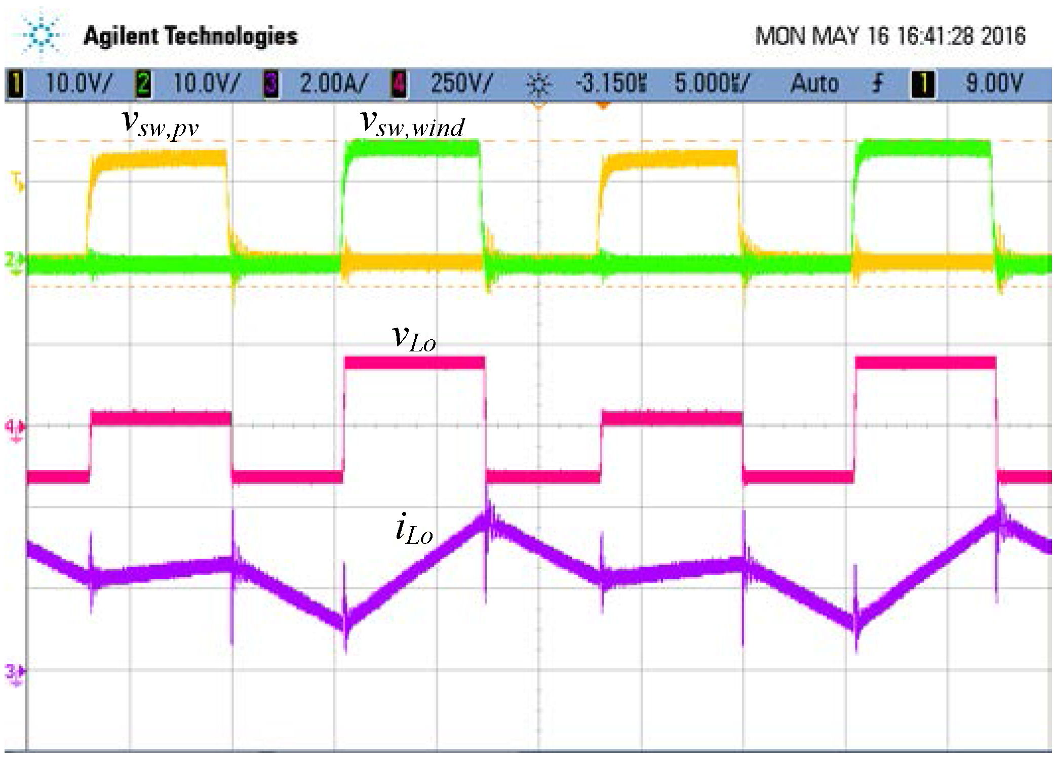
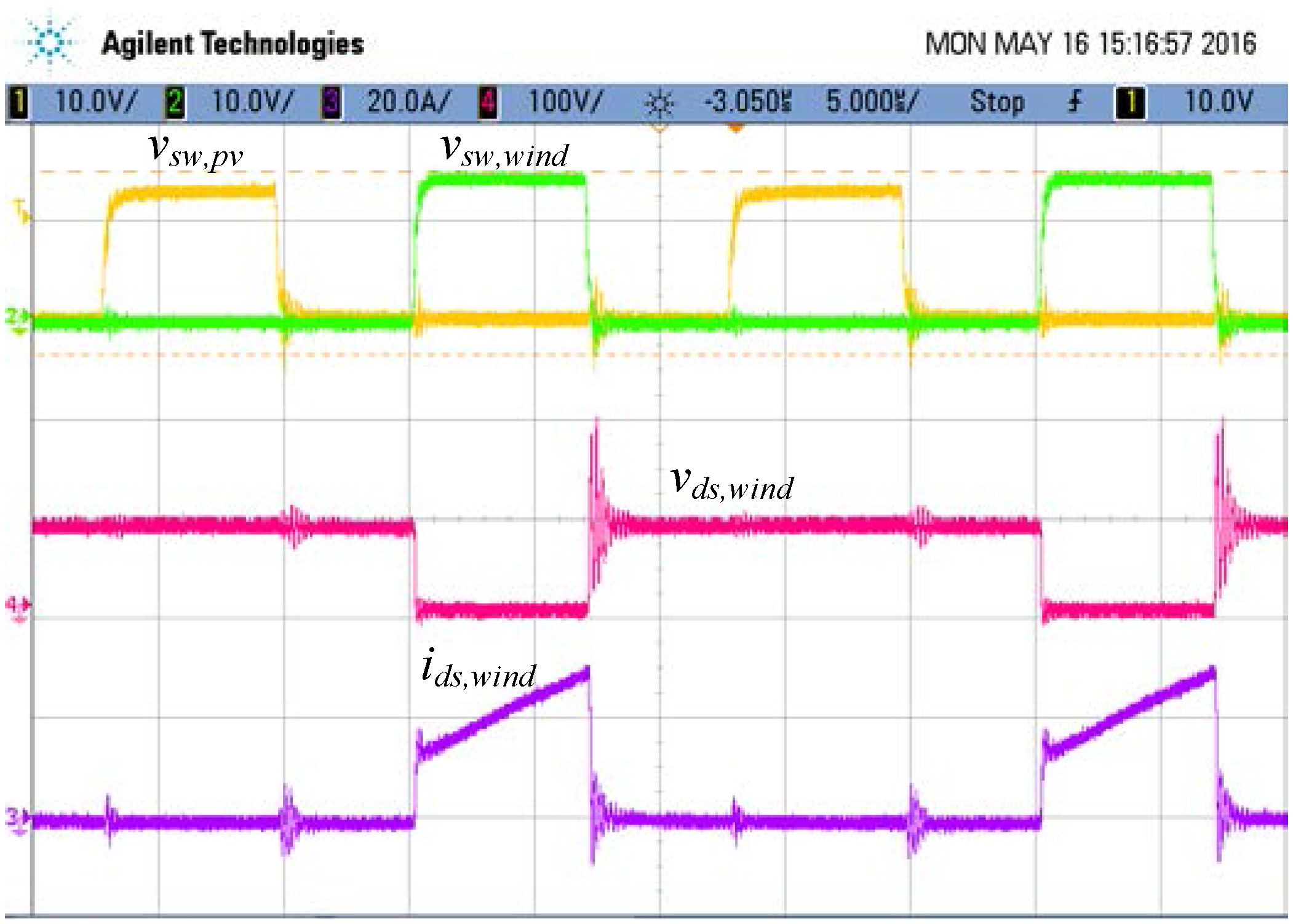
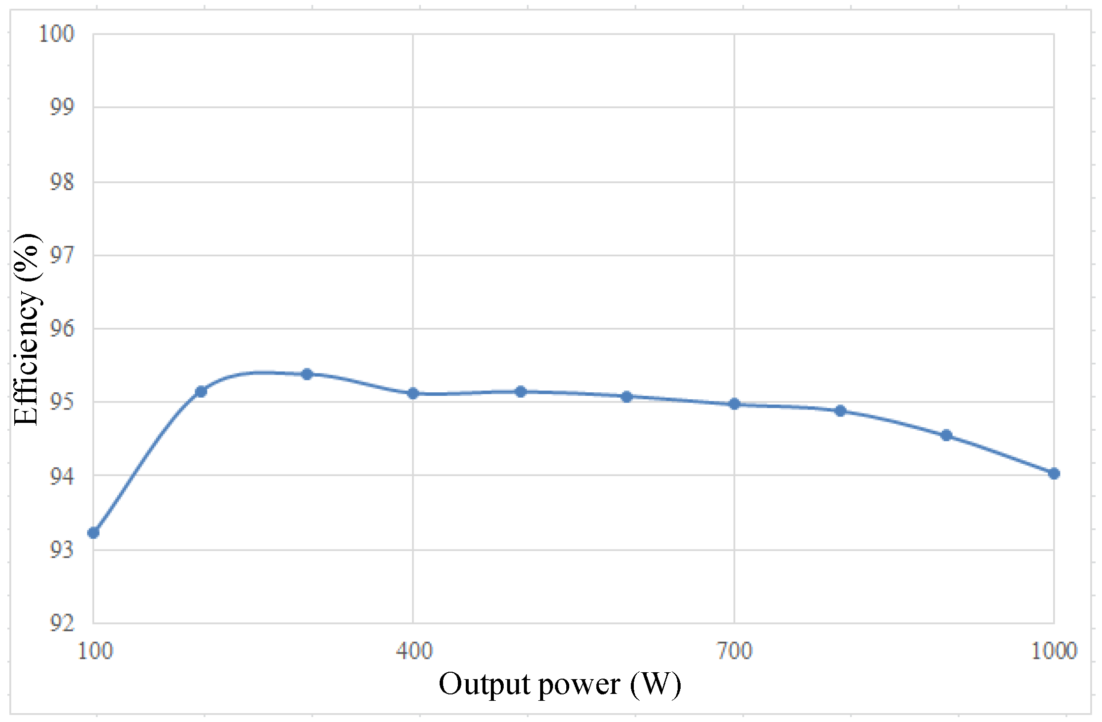
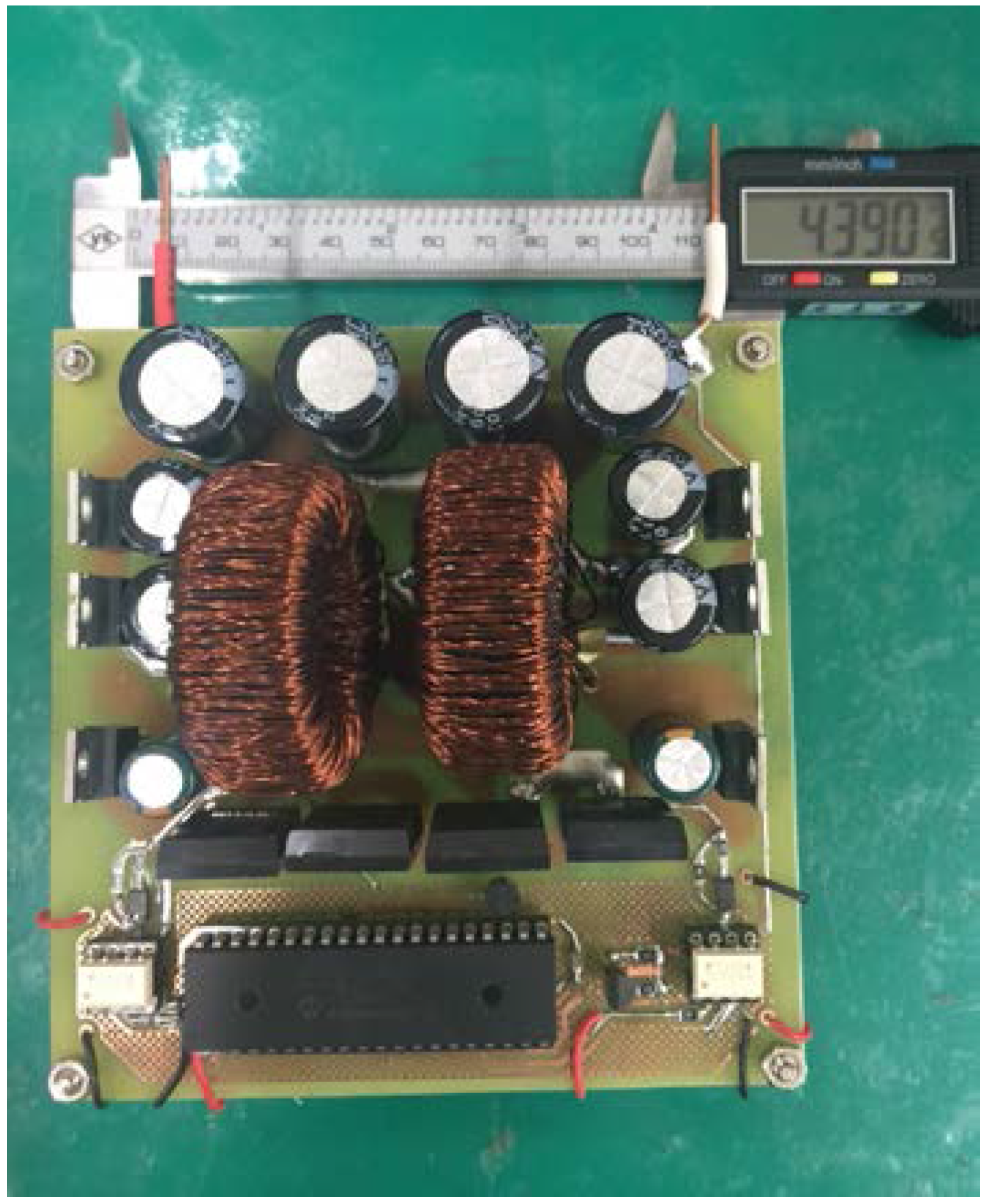
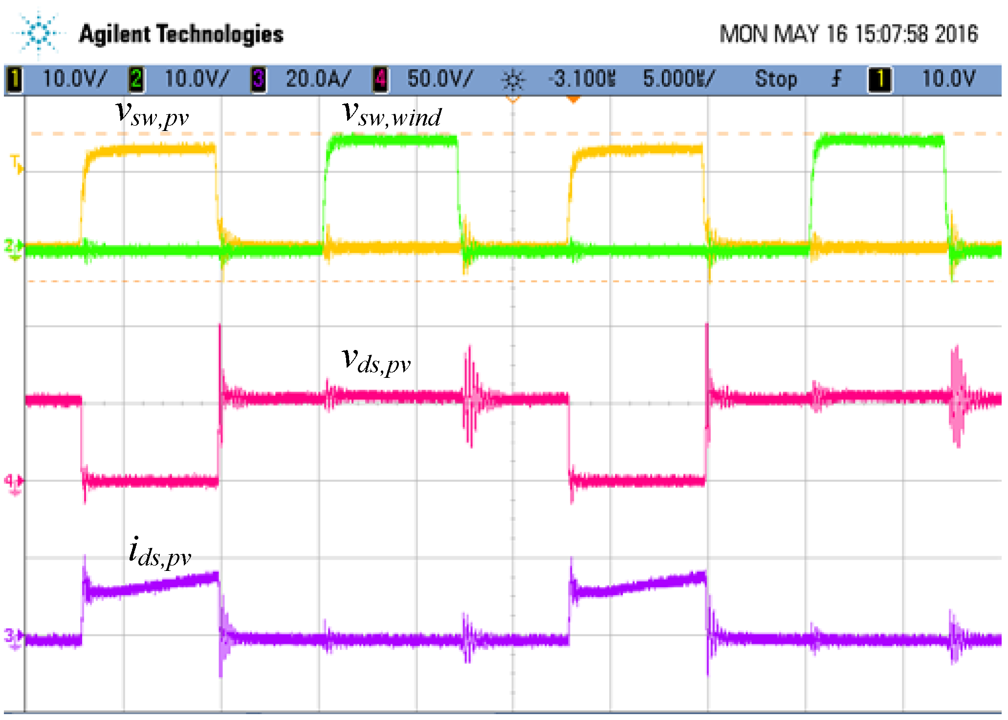
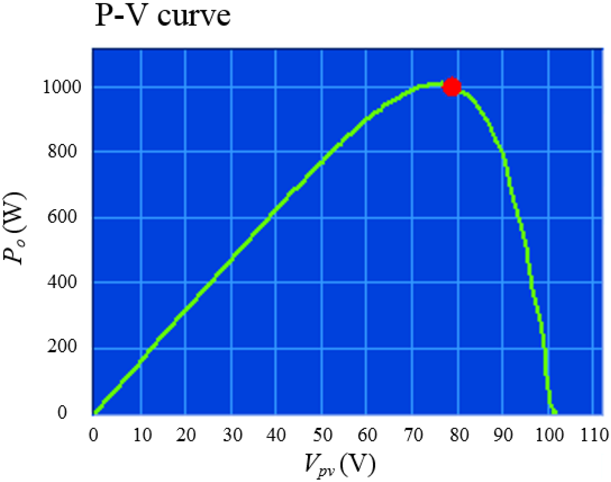
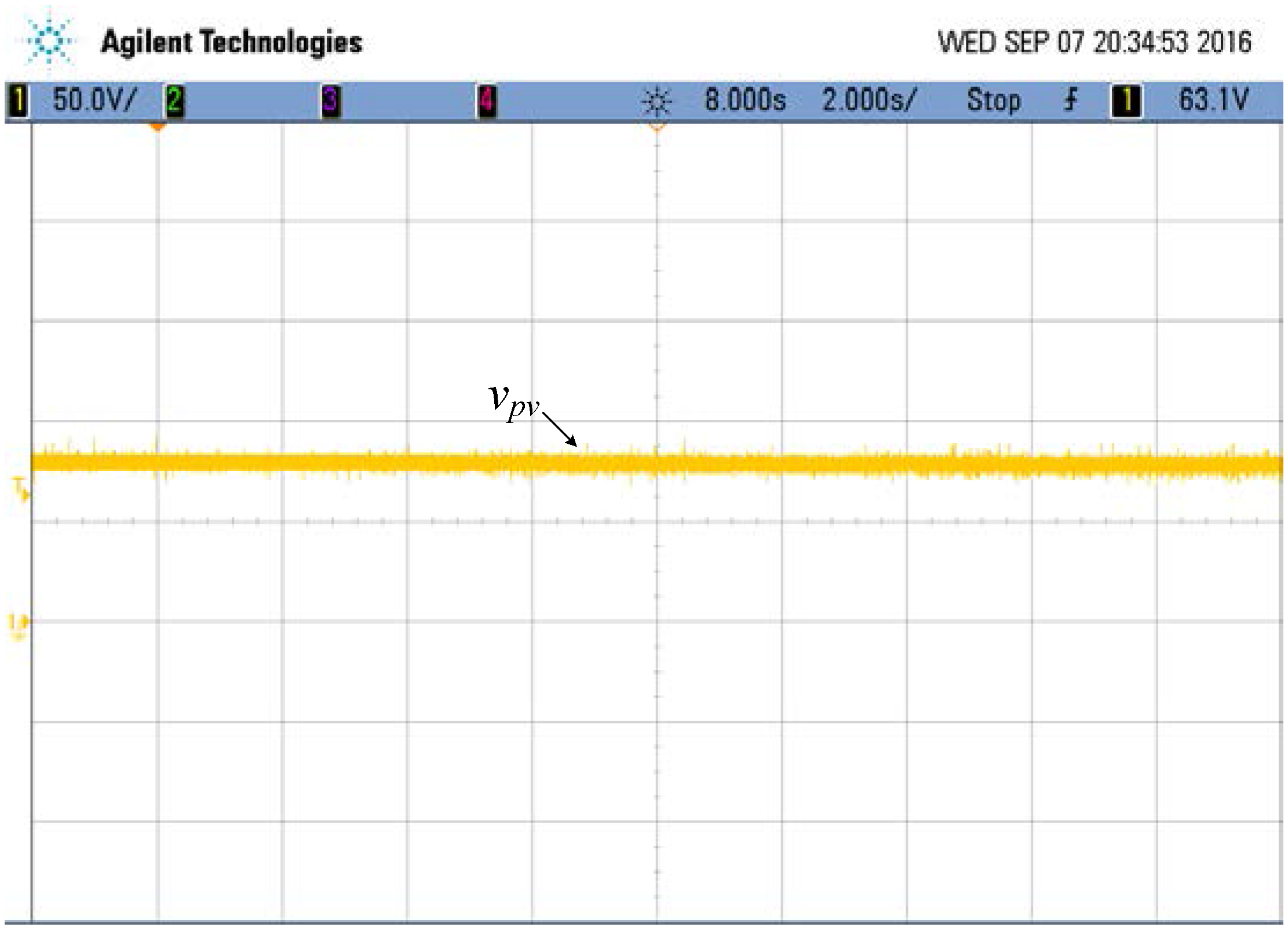
5. Experimental Results
To verify the correctness of the theoretical analysis in this paper, a 1-kW prototype with the specifications summarized in Table 2 is built. The output inductor Lo is designed according to Section 4, which ensures CCM operation while output power is greater than 500 W. In Figure 7, the output power Po is equal to 500 W. It can be seen that the inductor current iLo is twice the switching frequency and in BCM. This experimental measurement of iLo and inductor voltage vLo are identical to the conceptual waveforms depicted in Figure 6. Output power can be increased by enlarging the duty ratios of active switches. At 1-kW output, Figure 8 shows that the control signals vsw,pv and vsw,wind are still in an interleaved pattern but with larger duty ratio than that in Figure 7. In addition, the inductor current iLo is, indeed, in CCM. To examine the voltage and current stresses of the active switch, Figure 9 shows the practical voltage vds,wind and current ids,wind at full load, while vds,pv and ids,pv are shown in Figure 10. The vds,wind and ids,wind stand for the voltage and current of the active switches SW1,wind and SW2,wind, as vds,pv and ids,pv do for SW1,pv and SW2,pv. Figure 11 indicates that the output voltage can be kept at 400 V with the designed inductance, even if one of the renewable power sources shuts down. The DIPWC is able to accomplish a high conversion efficiency. Figure 12 depicts the measured efficiency from light load to full load, in which the peak efficiency is up to 95.4%. The practical measurement of the MPPT result at full load is shown in Figure 13. After MPPT, Figure 14 shows the steady-state output voltage of the PV module, vpv, from which it can be seen that the output voltage fluctuates around a constant. In addition, Figure 15 is the picture of the DIPWC setup.
Table 2.
The specifications of the DIPWC.
Figure 7.
Measured waveforms while the output power is 500 W (vsw,wind: 10 V/div, vsw,pv: 10 V/div, vLo: 200 V/div, iLo: 2 A/div, time: 5 μs/div).
Figure 8.
Measured waveforms while the DIPWC is operated at full load (vsw,wind: 10 V/div, vsw,pv: 10 V/div, vLo: 250 V/div, iLo: 2 A/div, time: 5 μs/div).
Figure 9.
Measured waveforms of active switches at wind-turbine input port while the output power is 1 kW (vsw,wind: 10 V/div, vsw,pv: 10 V/div, vds,wind: 100 V/div, ids,wind: 20 A/div, time: 5 μs/div).
Figure 10.
Measured waveforms of active switches at the PV input port while the output power is 1 kW (vsw,wind: 10 V/div, vsw,pv: 10 V/div, vds,pv: 50 V/div, ids,pv: 20 A/div, time: 5 μs/div).
Figure 11.
Measured waveforms to illustrate the transient response of the DIPWC (vsw,wind: 10 V/div, vsw,pv: 10 V/div, vLo: 200 V/div, iLo: 2 A/div, time: 5 μs/div).
Figure 12.
The measured efficiency from light load to full load.
Figure 13.
The practical MPPT result of the DIPWC at full load.
Figure 14.
Output voltage of the PV module after MPPT and in steady state (vpv: 50 V/div, time: 2 s/div).
Figure 15.
Picture of the DIPWC.
6. Conclusions
A novel DIPWC to process PV energy and wind-turbine power is first presented and then its operation principle is explored. The key power component in the DIPWC is the output inductor, which is designed with a detailed and theoretical derivation. To verify the correctness, a 1-kW prototype with the designed values is built and measured. Practical results validate the DIPWC. In addition, the feasibility and high-efficiency feature are also illustrated by the measurements.
Acknowledgments
The authors would like to convey their appreciation for grant support from the Ministry of Science and Technology (MOST) of Taiwan under its grant with reference number MOST 104-2221-E-327-036.
Author Contributions
Chih-Lung Shen and You-Sheng Shen conceived and designed the circuit. You-Sheng Shen performed simulations, carried out the prototype, and analyzed data with the guidance from Chih-Lung Shen. Chih-Lung Shen revised the manuscript for submission.
Conflicts of Interest
The authors declare no conflict of interest.
References
- Alireza, K.; Mohamed, Y.A.R.I. Networked-based hybrid distributed power sharing and control for islanded microgrid systems. IEEE Trans. Power Electron. 2015, 30, 603–617. [Google Scholar]
- Chunhua, P.; Peng, X.; Lei, P.; Rong, Y. Flexible robust optimization dispatch for hybrid wind/photovoltaic/hydro/thermal power system. IEEE Trans. Smart Grid. 2016, 7, 751–762. [Google Scholar]
- Hussein, M.M.; Senjyu, T.; Orabi, M.; Wahab, M.A.A.; Hamada, M.M. Control of a stand-alone variable speed wind energy supply system. Appl. Sci. 2013, 3, 437–456. [Google Scholar] [CrossRef]
- Yamada, H.; Kimura, K.; Hanamoto, T.; Ishiyama, T.; Sakaguchi, T.; Takahashi, T. A novel MPPT control method of thermoelectric power generation with single sensor. Appl. Sci. 2013, 3, 545–558. [Google Scholar] [CrossRef]
- Lai, C.-M.; Yang, M.-J. A high-gain three-port power converter with fuel cell, battery sources and stacked output for hybrid electric vehicles and DC-microgrids. Energies 2016, 9, 180. [Google Scholar] [CrossRef]
- Ramalu, T.; Mohd Radzi, M.A.; Mohd Zainuri, M.A.A.; Abdul Wahab, N.I.; Abdul Rahman, R.Z. A photovoltaic-based sepic converter with dual-fuzzy maximum power point tracking for optimal buck and boost operations. Energies 2016, 9, 604. [Google Scholar] [CrossRef]
- Liu, F.; Wang, Z.; Mao, Y.; Ruan, X. Asymmetrical half-bridge double-input DC/DC converters adopting pulsating voltage source cells for low power applications. IEEE Trans. Power Electron. 2014, 29, 4741–4751. [Google Scholar] [CrossRef]
- Sun, X.; Zhou, Y.; Wang, W.; Wang, B.; Zhang, Z. Alternative source-port-tolerant series-connected double-input DC–DC converter. IEEE Trans. Power Electron. 2015, 30, 2733–2742. [Google Scholar] [CrossRef]
- Banaei, M.R.; Ardi, H.; Alizadeh, R.; Farakhor, A. Non-isolated multi-input–single-output DC/DC converter for photovoltaic power generation systems. IET Trans. Power Electron. 2014, 7, 2806–2816. [Google Scholar] [CrossRef]
- Yang, P.; Chi, K.T.; Xu, J.; Zhou, G. Synthesis and analysis of double-input single-output DC/DC converters. IEEE Trans. Ind. Electron. 2015, 62, 6284–6295. [Google Scholar] [CrossRef]
- Tsai, C.-T.; Shen, C.-L.; Su, J.-C. A power supply system with ZVS and current-doubler features for hybrid renewable energy conversion. Energies 2013, 6, 4859–4878. [Google Scholar] [CrossRef]
- Piegari, L.; Rizzo, R.; Spina, I.; Tricoli, P. Optimized adaptive perturb and observe maximum power point tracking control for photovoltaic generation. Energies 2015, 8, 3418–3436. [Google Scholar] [CrossRef]
- Park, S.; Park, Y.; Choi, S.; Choi, W.; Lee, K.-B. Soft-switched interleaved boost converters for high step-up and high-power applications. IEEE Trans. Power Electron. 2011, 26, 2906–2914. [Google Scholar] [CrossRef]
- Hu, Y.; Deng, Y.; Long, J.; Lu, X. High step-up passive absorption circuit used in non-isolated high step-up converter. IET Trans. Power Electron. 2014, 7, 1945–1953. [Google Scholar] [CrossRef]
- Li, W.; Xiang, X.; Li, C.; Li, W.; He, X. Interleaved high step-up ZVT converter with built-in transformer voltage doubler cell for distributed PV generation system. IEEE Trans. Power Electron. 2013, 28, 300–313. [Google Scholar] [CrossRef]
- Liu, H.; Li, F.; Ai, J. A novel high step-up dual switches converter with coupled inductor and voltage multiplier cell for a renewable energy system. IEEE Trans. Power Electron. 2016, 31, 4974–4983. [Google Scholar] [CrossRef]
- Liu, H.; Li, F. a novel high step-up converter with a quasi-active switched-inductor structure for renewable energy systems. IEEE Trans. Power Electron. 2016, 31, 5030–5039. [Google Scholar] [CrossRef]
- Shen, C.-L.; Chiu, P.C. Buck-boost-flyback integrated converter with single switch to achieve high voltage gain for PV or fuel-cell applications. IET Trans. Power Electron. 2016, 9, 1228–1237. [Google Scholar] [CrossRef]
- Tseng, S.-Y.; Wang, H.-Y. A photovoltaic power system using a high step-up converter for DC load applications. Energies 2013, 6, 1068–1100. [Google Scholar] [CrossRef]
- Shen, C.-L.; Chen, H.-Y.; Chiu, P.-C. Integrated three-voltage-booster DC-DC converter to achieve high voltage gain with leakage-energy recycling for PV or fuel-cell power systems. Energies 2015, 8, 9843–9859. [Google Scholar] [CrossRef]
- Lai, C.-M. Development of a novel bidirectional DC/DC converter topology with high voltage conversion ratio for electric vehicles and DC-microgrids. Energies 2016, 9, 410. [Google Scholar] [CrossRef]
- Chen, Y.-M.; Liu, Y.-C.; Wu, F.-Y. Multi-input DC/DC converter based on the multiwinding transformer for renewable energy applications. IEEE Trans. Ind. Appl. 2002, 38, 1096–1104. [Google Scholar] [CrossRef]
- Shi, X.; Jiang, J.; Guo, X. An efficiency-optimized isolated bidirectional DC-DC converter with extended power range for energy storage systems in microgrids. Energies 2013, 6, 27–44. [Google Scholar] [CrossRef]
- Abramovitz, A.; Liao, C.-S.; Smedley, K. State-plane analysis of regenerative snubber for flyback converters. IEEE Trans. Power Electron. 2013, 28, 5323–5332. [Google Scholar] [CrossRef]
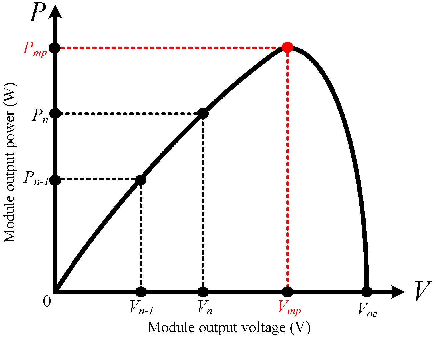
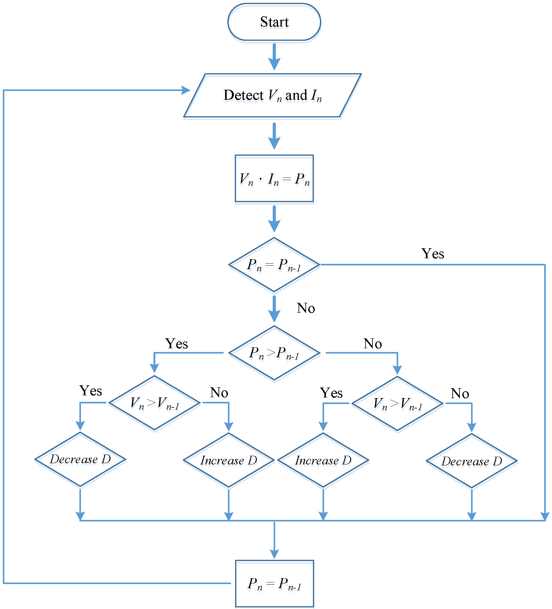
© 2016 by the authors; licensee MDPI, Basel, Switzerland. This article is an open access article distributed under the terms and conditions of the Creative Commons Attribution (CC-BY) license (http://creativecommons.org/licenses/by/4.0/).