Article

Three-Phase PV CHB Inverter for a Distributed Power Generation System

Department of Electrical Engineering and Information Technology, University of Napoli Federico II, Via Claudio 21, Napoli 80125, Italy
*
Author to whom correspondence should be addressed.
Appl. Sci. 2016, 6(10), 287; https://doi.org/10.3390/app6100287
Submission received: 14 July 2016 / Revised: 23 September 2016 / Accepted: 27 September 2016 / Published: 11 October 2016
(This article belongs to the Special Issue Advancing Grid-Connected Renewable Generation Systems)

Abstract

:
This work deals with the design of a three-phase grid-tied photovoltaic (PV) cascade H-bridge inverter for distributed power conversion. The power balancing among the phases must be properly addressed. In fact, an intra-phase power imbalance—arising from uneven irradiance and temperature conditions—generates a per-phase power imbalance. This latter can be compensated by the injection of a proper zero-sequence voltage, while the intra-phase balance is ensured by means of a hybrid modulation method which is able to guarantee the handling of unequal DC (Direct Current) sources, stable circuit operation, and maximization of PV power production. The digital controller is developed and tested in Matlab/Simulink environment integrated with XSG (Xilinx System Generator), thus allowing an easy transfer on a field-programmable gate array (FPGA) platform and accurately describing the behavior of a real hardware implementation. Thus, numerical results have been considered to prove the effectiveness of the proposed approach.

Graphical Abstract

1. Introduction

During the last decade, photovoltaic (PV) energy conversion has become a fully mature technology, giving (in many countries) an impressive contribution to sustain the electricity demand. Its worldwide diffusion has also been supported by the increased reliability of power converters (henceforth PV inverters) which interface solar systems with the utility grid. The role of PV inverters is of utmost importance for the overall suitability of photovoltaic energy, because they manage energy exchange between solar panels and utility grid by guaranteeing (i) maximum conversion efficiency and (ii) high quality of delivered electricity. The first task is performed by means of Maximum Power Point Tracking (MPPT) algorithms that—by adjusting the switching operation of the power devices forming the converter—allow the PV system to always work with the optimum load. The second task, which consists of delivering “pure” sinusoidal currents with assigned parameters, is pursued by means of proper signal processing strategies.
Although a wide variety [1] of PV inverter topologies have been proposed so far, all of them can be roughly classified with respect to the number of independent inputs and to the size of the PV generators supplying each of them (DC (Direct Current) side) into two main categories, adopting, respectively, “centralized” conversion approaches or “distributed” conversion approaches. By recalling that an arbitrary large PV field is always built up by interconnecting many elemental PV generators, centralized conversion schemes are those where a single-input inverter serves many PV generators [2,3]. This solution has indubitable strengths; indeed, it minimizes the number of power devices (thus increasing both reliability and conversion efficiency), simplifies cabling, and so on. The weaknesses depend on the fact that when mismatches among operating conditions of the PV generators occur, power production can be adversely affected; in fact, as is widely known [4,5], the worst performing generator limits the performance of the whole photovoltaic system. In order to overcome this issue, it is possible to partition the solar field into subfields, each connected to a dedicated PV inverter. This approach can be driven up to equipping each solar panel with its own DC–DC [6,7,8,9] or DC–AC (Alternate Current) converter [10,11,12]. In this case, the yield of the PV system increases during mismatch conditions, but is adversely affected during normal operation (when no mismatches occur), because of the power dissipation across the increased number of switching devices; moreover, the need for a high voltage gain often requires the adoption of a double-stage converter topology, with a DC–DC stage providing gain, followed by the DC–AC conversion.
On the other hand, a significant effort has been paid in recent decades to improve the conversion features (e.g., efficiency, total harmonic distortion, and so on) of the grid-tied inverters (AC side). In particular, recent literature proves the effectiveness of some multilevel approaches [13,14]. Although the appealing advantages provided by both the classical topologies, such as Neutral Point Clamped (NPC) and Flying Capacitor (FC) [15], and by the recent Crossover Switches Cell (CSC) [16] and PUC5 [17], only Cascaded H-Bridge (CHB) [15,18] is suited for multiple isolated DC-sources [19], thus joining the best features of both distributed and centralized approaches, while implementing a multilevel conversion.
In particular, Cascaded H-Bridge (CHB) multilevel PV inverters [20,21,22,23,24] are composed of several “smaller” (in terms of rated power) full-bridge DC–AC converters (hereafter referred as cells), each of them made by downsized switching devices, which are therefore less affected by dynamic and static power losses. Moreover [25], thanks to ability of multilevel topologies to produce “stepped” output voltages, CHB inverters reproduce sinusoidal waveforms better than conventional full-bridge inverters with less filter efforts, the total harmonic distortion (THD) being a function of the number of discrete voltage levels exploited to synthesize the output waveform [26]. Moreover, the modular structure of CHB inverters is naturally well-suited for distributed power conversion, because each cell can be powered by a small PV generator and perform a dedicated MPPT [20].
Despite of the aforementioned advantages, in CHB inverters, the control of electronic devices switching operation is much more demanding compared to conventional inverters. Moreover, the increased number of switching devices requires an accurate evaluation of power consumption during turn-on and turn-off transients [27], which affects the conversion efficiency. In a recent paper [28], a single-phase CHB multilevel PV inverter suitable for high granularity maximum power point tracking (up to single panel level) was presented. The innovative control strategy adopted therein allowed only one elemental converter to work in switching mode while the others were kept either “ON” or “OFF” (see next section).
The proposed three-phase CHB adopts a mixed staircase-pulse-width modulation (PWM) [28,29,30,31,32,33] strategy that drives only one power cell at time to work in PWM, while all other cells provide a constant output voltage. Output voltages achieved by each cell can be independently adjusted so that the maximum power point (MPP) of each PV subsystem (connected to the corresponding cell of the inverter) can be individually tracked. The number of sections can coincide with the number of solar panels forming the PV system; thus, single panel MPPs can be individually adjusted, and the proposed approach can be effectively adopted for single panel distributed conversion schemes.
In order to extend this modulation strategy to a three-phase system, the injection of a proper zero-sequence voltage is adopted to avoid the per-phase power imbalance due to unevenly operating PV generators (i.e., intra-phase power imbalance). In fact, the per-phase power imbalance leads to unbalanced three-phase currents, not acceptable in grid connected application. To this aim, a cascaded PI (Proportional Integral) control was implemented, comprising an outer control loop regulating the overall DC-link voltage and an inner control loop accounting for the regulation of direct and reactive grid currents by means of a multivariable PI controller [34]. This latter ensures that d and q components are almost fully decoupled, while allowing a simple implementation and assuring fast dynamics and zero steady-state error. Even though effective approaches which concern optimal control strategies of power balancing have been proposed in recent literature [35,36,37], the adopted choice reaches the goal of proving the compatibility of the proposed modulation strategy with traditional and commonly adopted control techniques.
The paper is organized as follows: in Section 2, the proposed circuit topology is described and the mathematical model for controlling its operation is presented; in Section 3, the control strategy, along with the proposed CHB inverter implemented in Matlab/Simulink® are shown, and numerical results are discussed to verify the effectiveness of the proposed approach in static and dynamic conditions, even under partial shading. Conclusions are drawn in Section 4.

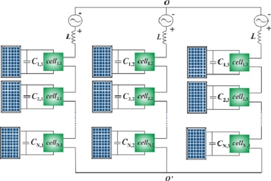
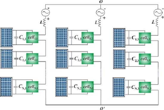
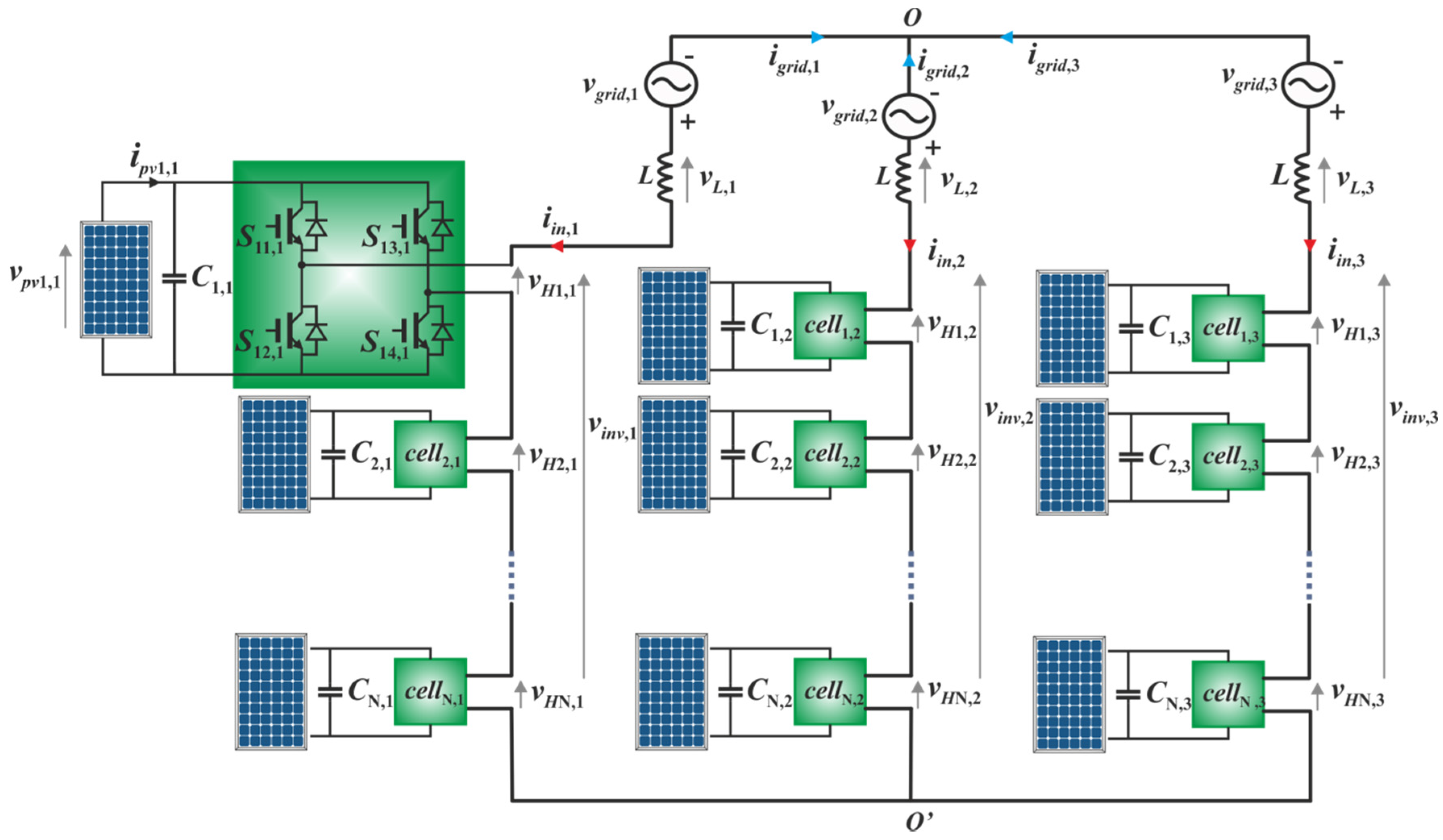
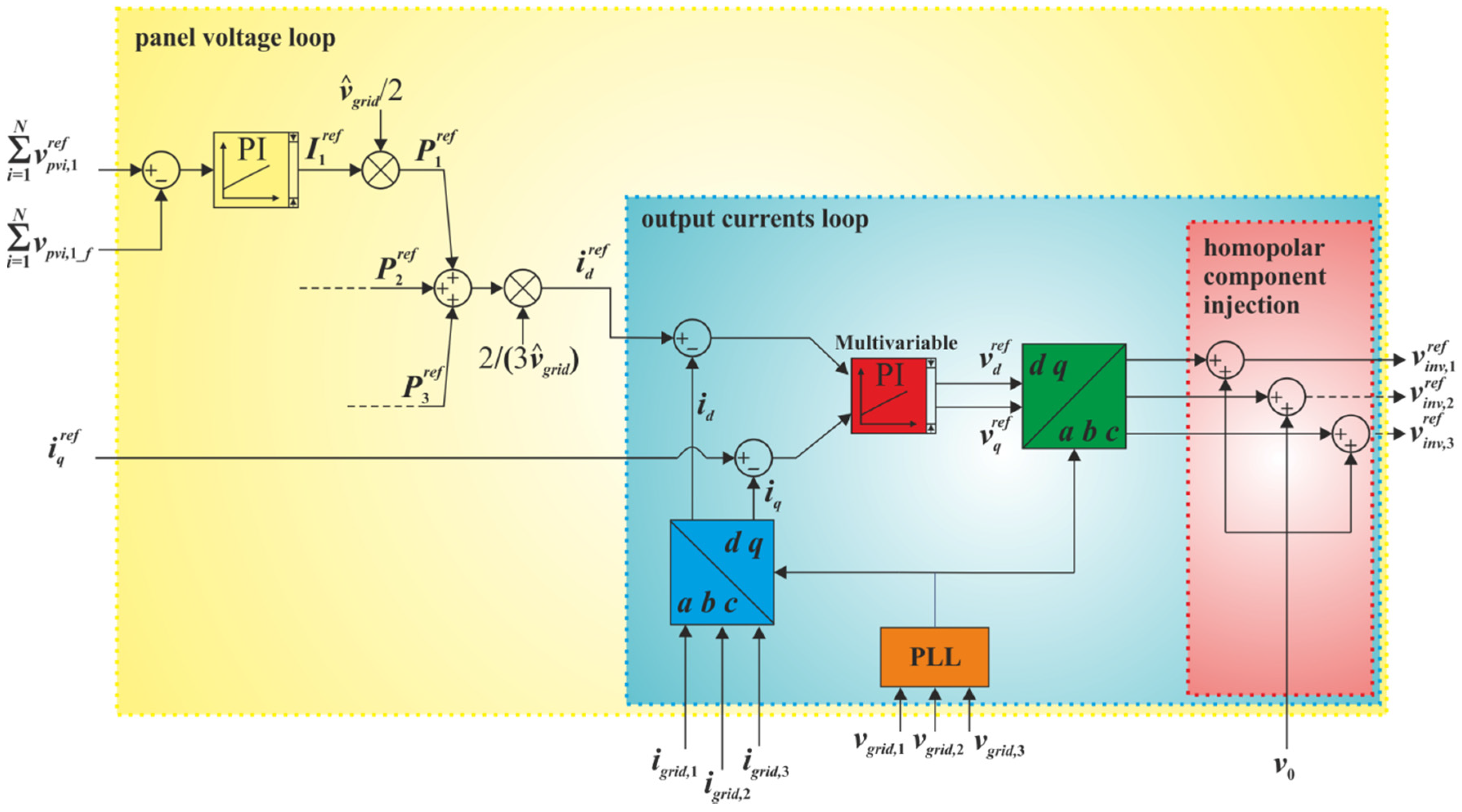
2. System Topology and Control Strategy

The three-phase topology of the multilevel CHB inverter analyzed in this paper is shown in Figure 1. As can be seen, it is made by N series connected cells for each phase leg. Each cell is a H-bridge inverter powered by a photovoltaic generator, where the PV generator can be either a single solar panel or a PV subsystem. The output waveform for each leg is the sum of the output voltages (vHi,p, with i = 1, …, N, and p = 1, 2, 3) of each H-bridge. An inductive filter L is exploited to filter the undesired harmonic components in the grid current.
The control strategy we propose has a twofold main objective: (i) adjusting the input voltage of each cell to track the MPP of the corresponding PV generator; (ii) driving only one cell at time in PWM mode in order to reduce switching losses.
The core of the control strategy is a specially-suited sorting algorithm that establishes which cell must work in PWM mode while the others are kept in a fixed state, the overall constraints being the sum of the input voltages (which must exceed the utility grid peak voltage) and the phase relation among the three legs.
The control algorithm compares the errors between the MPPT reference values and the voltages actually measured across each PV generator, with the aim of driving only one cell in PWM mode, while the others can be either connected or bypassed, according to the detailed analysis reported below.

2.1. CHB Inverter Modeling

From Figure 1, it can be argued that for a given voltage vpvi,p across the ith DC-link capacitor, the ith cell in the p-th leg provides an output voltage vHi,p which can assume only three values (0, +vpvi,p, −vpvi,p) depending on the state of the four switches Sis,p. Namely, vHi,p = 0 if either Si1,p and Si3,p or Si2,p and Si4,p are in the ON state; vHip = +vpvi,p when both Si1,p and Si4,p are ON; vHi,p = −vpvi,p when both Si2,p and Si3,p are ON. As a result, the AC vinv,p waveform is composed by 2N + 1 levels given by the sum of the voltages vHi,p.
In other terms, by assuming the switch states as binary signals (i.e., switch ON corresponds to 1, while switch OFF corresponds to 0), the AC voltage vinv,p across the p-th phase can be written as follows:
v i n v , p = i = 1 N v H i , p = i = 1 N ( S i 1 , p S i 3 , p ) v p v i , p = i = 1 N h i , p v p v i , p
where the modulation factor hi,p can assume three possible values (+1, −1, 0). It is worth noting that in conventional modulation approaches, the cells are either all modulated (as in the phase shifted PWM) [20,38,39,40,41], or none are modulated (as in the level-shifted modulation) [21]. Differently from those approaches, only one set of the modulation factors h is being modulated in our algorithm, so that (1) can be written as
v i n v , p = i = 1 K 1 ± ( v p v i , p ) + h K , p v p v K , p
where K identifies the only cell driven in PWM mode during each control cycle. The +/− sign in the sum depends on whether the corresponding h is kept to 1 or −1; the remaining N-K cells do not appear (i.e. h = 0). It can be noted from Figure 1 that the states defined by h = +/−1 correspond to the discharging of the DC-link capacitors Ci,p, while h = 0 makes the capacitor to be charged by the PV source. Whether the sign is + or - depends on whether vinv,p is in the positive half cycle or in the negative half cycle, respectively.
In order to write the open loop state equations for the control problem, it is possible to replace hi,p with a continuous switching function h ¯ i , p bounded in the interval [−1, +1]; thus, each leg current iin,p injected into the grid can be straightforwardly related to the voltages across each cell:
d i i n , p d t = v L , p L = v g r i d , p v i n v , p L = v g r i d , p i = 1 N h ¯ i , p v p v i , p L d v p v i , p d t = 1 C i , p ( i p v i , p + h ¯ i , p i i n , p ) i = 1 , . . , N p = 1 , 2 , 3
The control is achieved by feeding back the state variables according to the schematic view depicted in Figure 2. Figure 2 can be viewed as a quite “standard” control cycle which provides the reference voltages v i n v , p r e f for the three phases. For each phase, the outer loop adjusts the sum of the DC-link voltages vpv,i in accordance with the sum of the references v p v i , p r e f provided by the MPPT blocks (these blocks—not shown in the figure—perform a standard Perturb and Observe (P & O) algorithm). Unfortunately, in order to ensure the overall stability of the CHB inverter, the tracking voltage v p v i , p r e f should avoid the case that PV generators operate in the flat region of their I–V curve [42]. As a consequence, a lower boundary has to be defined, also ensuring a proper synthesis of AC-side multilevel waveform.
It important to note that the DC-link voltages vpv,i are obtained by digitally filtering the 100 Hz ripple, thus improving the quality of the inverter output current in terms of THD [20]. On the other hand, a proper sizing of the DC-link capacitors has been performed to limit the detrimental effect of the 100 Hz oscillation on the MPPT efficiency [1].
As can be seen, the first PI evaluates the reference currents I p r e f for each phase, and, from them, the reference active powers P p r e f .
In the inner loop, a multivariable PI controller [34] regulates both the direct and the reactive grid currents. To this end, the three reference powers given by the first PI are summed in order to get the direct current reference i d r e f , while the reactive current reference i q r e f can either be set to zero (in order to achieve unity power factor) or adjusted in order to control the reactive power. The adoption of a multivariable PI controller allows a simple implementation, while assuring fast dynamics and zero steady-state error for three-phase application.
Currents id and iq are achieved by converting the measured grid currents (abc coordinates) into dq coordinates. The outputs of the PI are the inverter reference voltages in dq coordinates, which are then converted to the three-phase reference voltages (abc coordinates); the synchronization of the dq transformation is performed by means of the phase-locked loop (PLL) circuit.
It is important to note that the independent MPP tracking performed for each cell may generate unbalanced phase power, thus inherently leading to unbalanced grid currents. In order to overcome this undesired drawback, a proper homopolar (zero-sequence) voltage component v0 is added to the direct sequence. Indeed, according to [43], for given power unbalances among the phases, defined as
Δ P p = P p r e f h = 1 3 P h r e f 3 p = 1 , 2
a voltage v0 allowing the inverter neutral point to move so as to have unbalanced inverter voltages (vinv,p in Figure 1), while assuring balanced grid currents, can be found in accordance with the following equations:
{ v ^ 0 = 4 3 i d r e f Δ P 1 2 + Δ P 1 Δ P 2 + Δ P 2 2 φ 0 = φ arctan [ 1 3 ( Δ P 2 Δ P 1 + 1 2 ) ]
where v ^ 0 and φ0 are, respectively, the peak value and the phase of v0, while φ is the phase of the balanced currents.
The reference voltages provided by the control scheme of Figure 3 are then converted into the gate signal commands (Sis,p in (1)) for the IGBTs (Insulated Gate Bipolar Transistor) of Figure 1. This is the innovative core of the present work, because it is at this stage that (thanks to a proper sorting algorithm) it is dynamically decided which cell of each leg has to be driven in PWM mode. Indeed, as is shown in Figure 3, the reference signal entering the PWM block depends on the index K, already defined in (2). The detailed description of the sorting algorithm is given below.

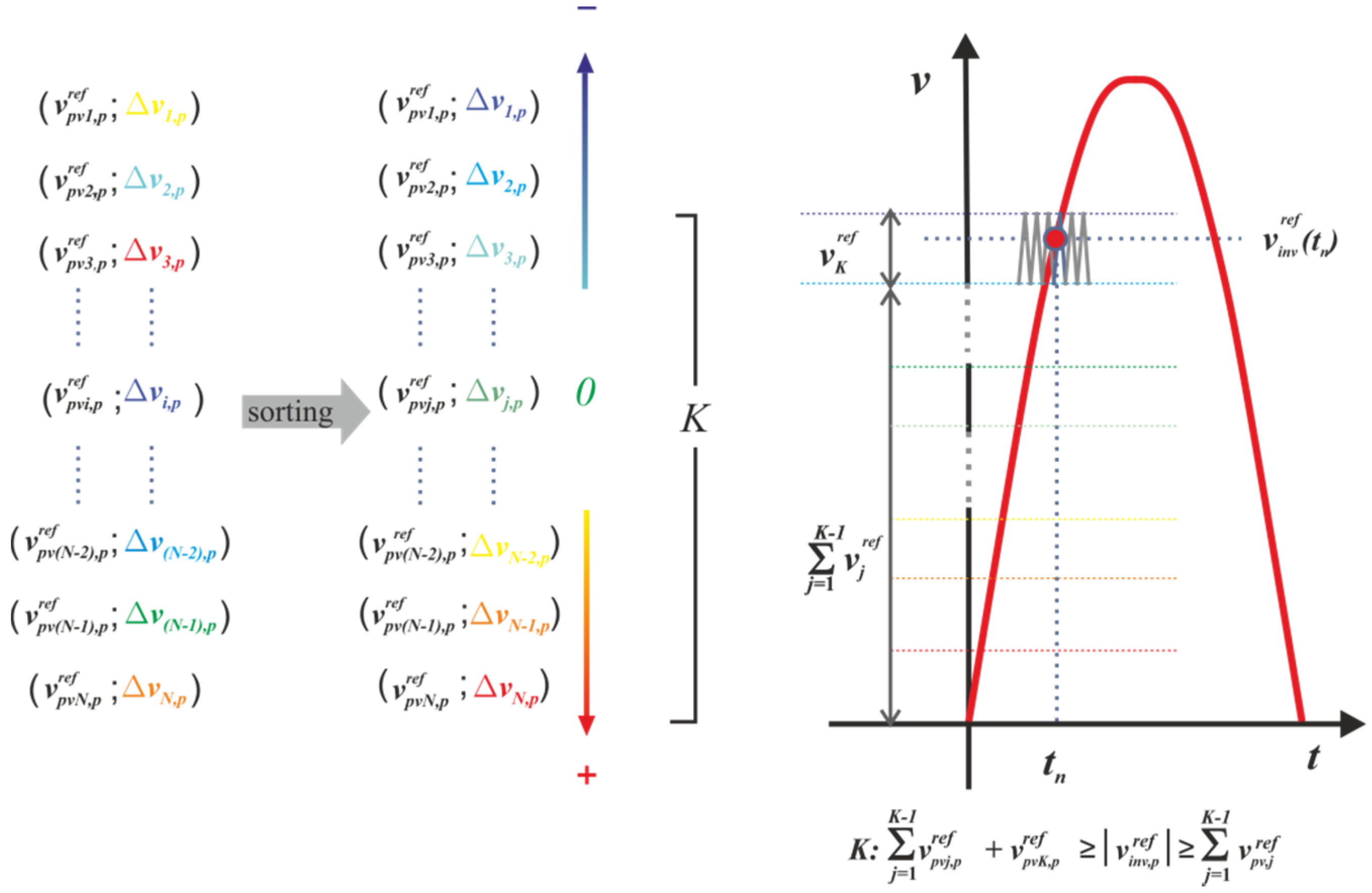
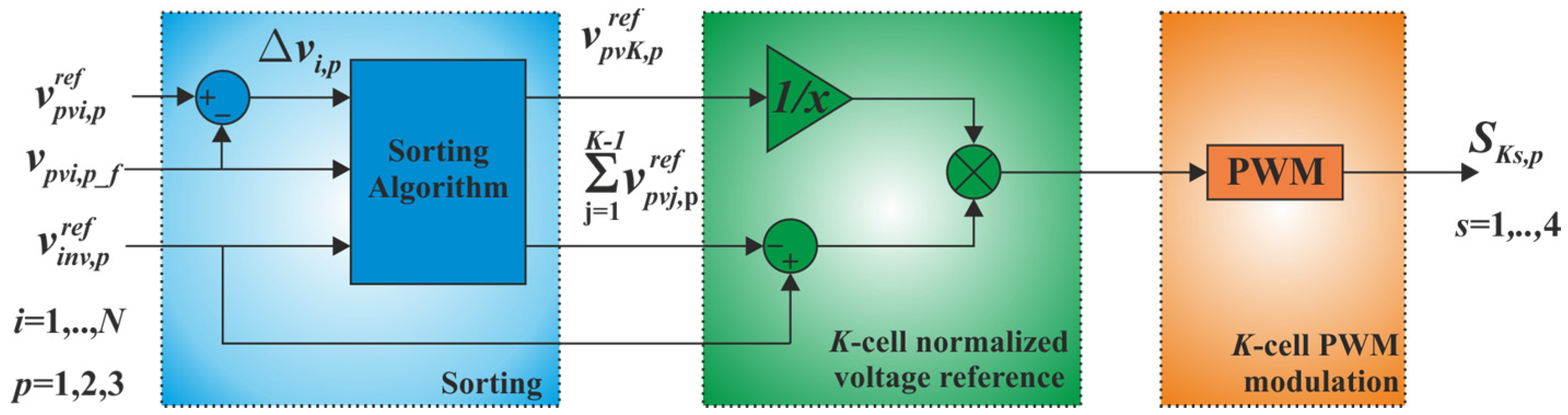
2.2. The Sorting Algorithm

According to (2), vinv,p can be synthesized by adding up the output voltages vHi of K-1 cells (by permanently connecting them) plus one cell in PWM mode, while the others are kept in the zero output voltage state. The new idea is to determine—in every control cycle—the state of each cell depending on the voltage error Δ v i , p = v p v i , p r e f v p v i , p _ f between the reference v p v i , p r e f given by the MPPTs and the filtered actual vpvi,p.
The algorithm is sketched in Figure 4.
The pairs ( v p v i , p r e f ; Δ v i , p ) are sorted in ascending order with respect to the voltage error, thus assigning the last position, N, to the cell with the highest positive error, while the first position, 1, is occupied by the cell with the lowest negative error (it is worth noting that the position in the sorted vector is not related to the position in the physical circuit). Then, according to the new order, the voltages v p v j , p r e f are added until the index K that makes true the following inequality is found:
j = 1 K 1 v p v j , p r e f + v p v K , p | v i n v , p | j = 1 K 1 v p v j , p r e f
The index K is the one already defined in (2); therefore, the first K-1 cells of the sorted vector (i.e., the cells with the lower voltage errors) have to be kept in the ±1 mode (discharging mode), the K-th cell has to be driven in PWM mode, and the last N-K cells (i.e., the cells with the higher voltage errors) have to be kept in the 0 mode (charging mode).
It should be noted that the modulation strategy is specially conceived for the CHB with unequal DC sources, exploiting small differences in the voltage of the individual power cells to reduce switching losses and improve the converter efficiency [19].

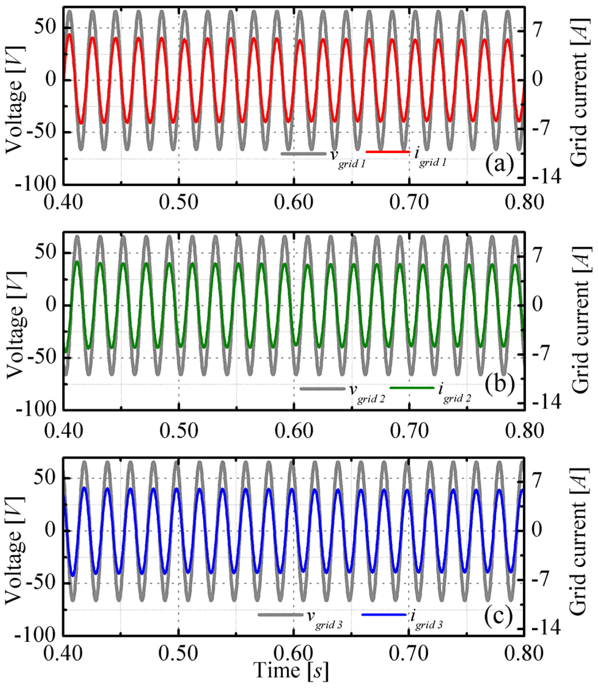
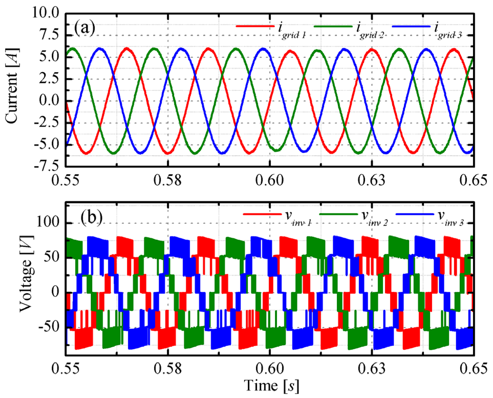
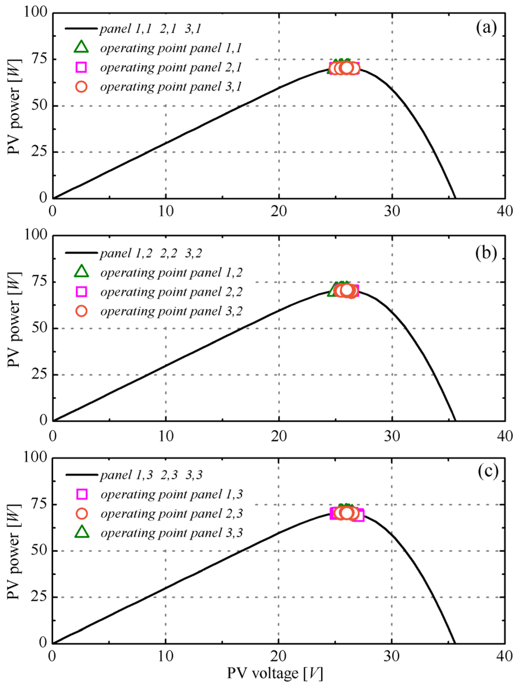
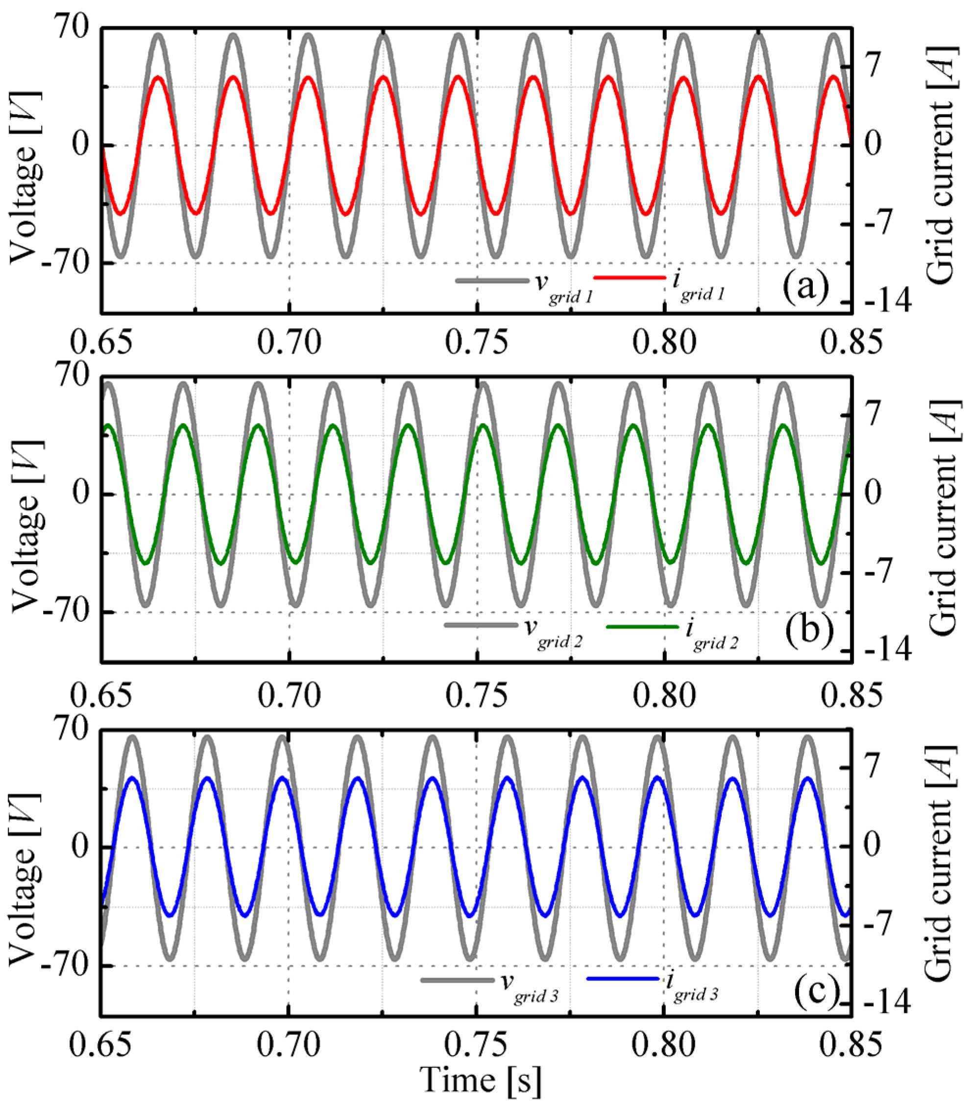
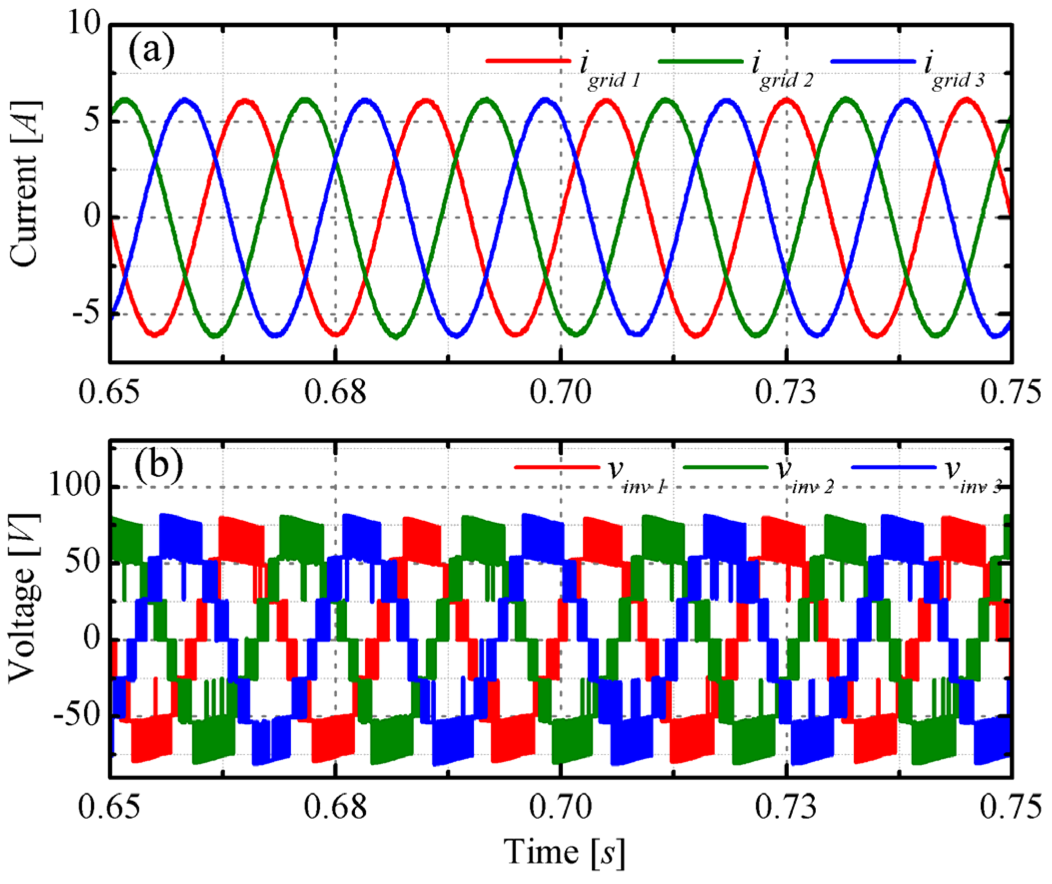
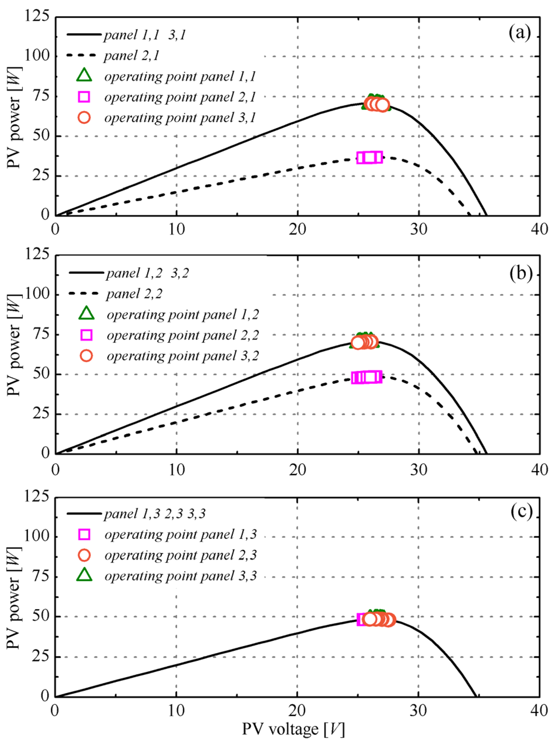
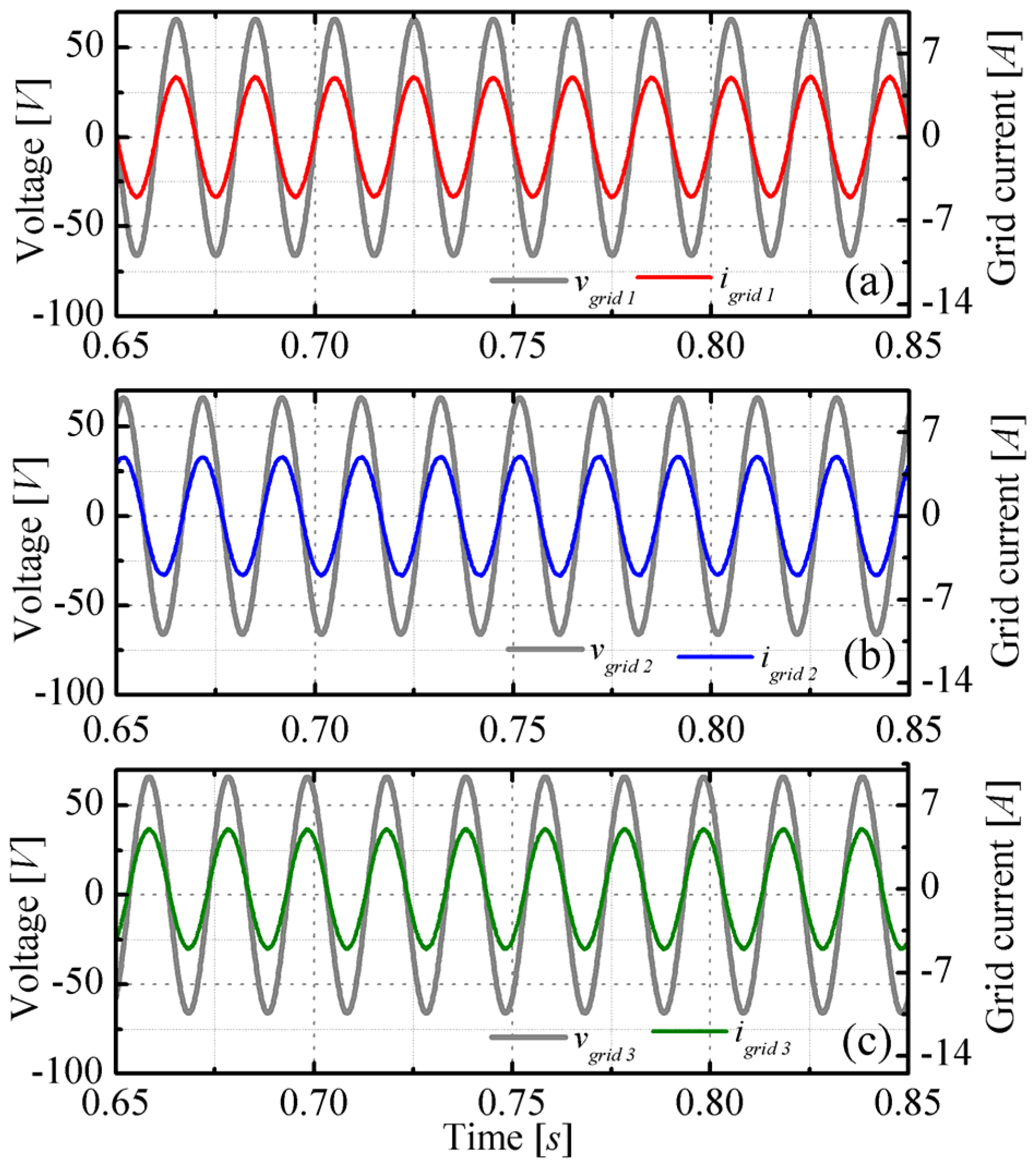
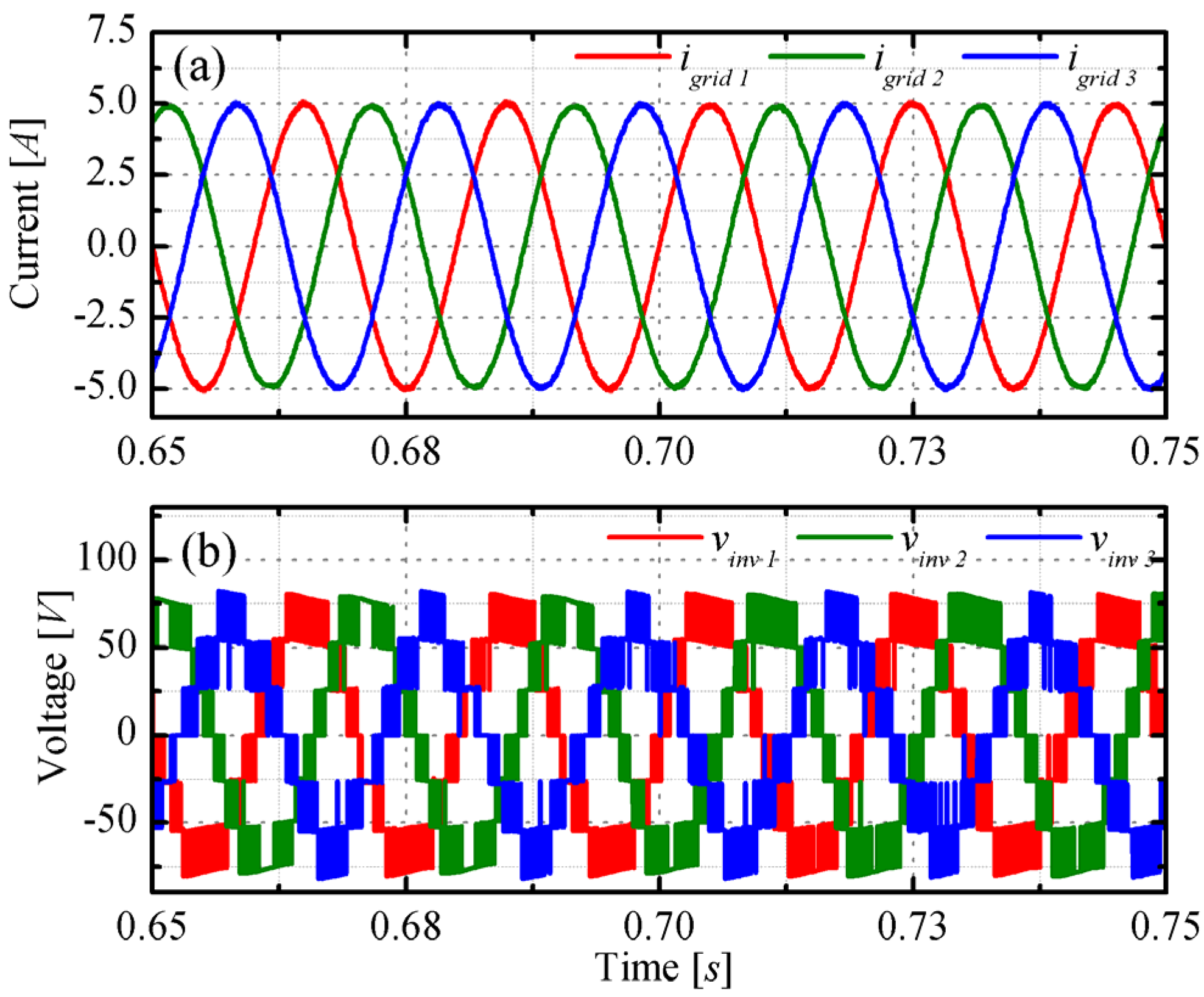
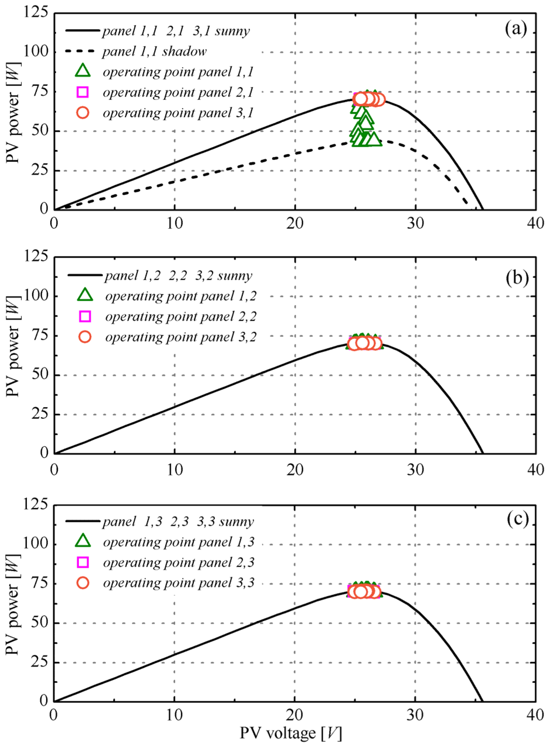
3. Numerical Analysis

The operation of the proposed topology and the control strategy described in the previous sections were analyzed by exploiting the Matlab Simulink® (2012a, Mathworks, Natick, MA, USA) environment. The simulated circuit was a three-phase system with three solar panels connected to each phase, each of them feeding a devised H-bridge, so that single-panel conversion was investigated. It was built by exploiting both specially suited elemental blocks taken from the Xilinx [44] library and custom homemade Verilog [45] modules. The main advantage of this approach is that the control code could be straightforwardly implemented on a Xilinx field-programmable gate array (FPGA) platform; moreover, it allowed very realistic simulations because the actual behavior of the hardware implementation of the control code on the FPGA was emulated by performing the circuit synthesis.
Table 1 reports the parameter of the simulated CHB inverter.
A detailed model for the PV panels, accurately describing the current voltage and the power voltage curves of commercially available solar modules [45] as a function of the illumination level and, eventually, of partial shading condition, was also adopted. Table 2 shows the details of PV panel models.
Three sets of operating conditions were analyzed: (i) uniform illumination over all solar panels; (ii) non-uniform illumination; (iii) dynamically changing illumination. The features that were monitored were the capability of tracking the MPP of individual solar panels, power balancing, and quality.
The first set of results is given in Figure 5, Figure 6 and Figure 7.
The curves shown in Figure 5a–c refer, respectively, to the three legs of the circuit. Since uniform illumination (625 W/m2) was considered, all of the P–V curves coincide each other; thus, for example, the P–V curves of the three solar panels connected to the first leg (Figure 5a) are represented by a unique curve.
Nevertheless, the maximum power points of the solar panels were independently tracked; therefore, the operating points actually assumed by each solar panel are shown by means of different symbols (squares, circles, triangles). As can be seen, all solar panels operate very close to their respective MPP, small oscillations being ascribable to the limit cycle of the P&O tracking algorithm.
The three grid currents—superposed to the respective grid voltages—are shown in Figure 6.
As can be observed, the power factor is unity, thus demonstrating the effectiveness of the active power transfer to the grid.
The reliability of the proposed approach can be better appreciated by looking at Figure 7, which shows the phase relation among the three currents (Figure 7a) and the modulated voltage waveforms produced by the sorting algorithm (Figure 7b). As can be seen, the voltages are synthesized by means of seven discrete levels, and the currents are symmetric and balanced; in this case (uniform illumination), the homopolar component vo (see Equation 4) is set to zero. The observed time interval of 100 ms corresponds to a MPPT period, while the switching frequency was f = 5 kHz. Moreover, the THD values of the phase currents and voltages have been calculated up to the 40th harmonic, as defined by the standard rules. The numerical results for the three-phase currents are 0.23%, 0.28%, and 0.27%, while for the modulated voltages they are 5.76%, 5.77%, and 6.40%.
The results gained when solar panels were not uniformly irradiated are reported in Figure 8, Figure 9 and Figure 10. In these experiments, the nine solar panels were subjected to the irradiance levels reported in Table 3, so that each of the three legs supplied a different power.
It can be observed from Figure 8 that—also in the case of partial shading—all solar panels operate at their respective MPP. What is now more challenging for the control system is to guarantee balanced grid currents, even if the supplied powers on the three legs were different from each other. The consequence of a power imbalance is that the outputs vinv,p of the multilevel inverters are also unbalanced. As explained in the previous section, the equilibrium of the three grid currents is achieved thanks to the addition of the homopolar voltage component vo. The effectiveness of this strategy is clearly visible in Figure 9, showing the superposition of the grid currents with the grid voltages, and Figure 10 showing the phase relation among the grid currents and the modulated voltages corresponding to three phase legs. In particular, from Figure 10b it can be seen that the zero-sequence injection provides no more balanced modulated voltages while assuring balanced currents. The THD values of the phase currents and voltages have been calculated up to the 40th harmonic, as for the uniform case. The numerical results are 0.60%, 0.68%, and 0.47% for the three-phase currents, while for the modulated voltages they are 5.60%, 6.00%, and 6.20%.
The last experiment was performed by linearly varying the irradiance impinging on the first solar panel of the first leg from 625 W/m2 to 400 W/m2 in a time interval starting at 0.4 s and ending at 0.8 s, so that the MPP of that panel changed from 73 W to 40 W. From Figure 11, we observe that the MPP of the shaded panel is correctly tracked during time; at the same time, the power factor is unity in all three legs (Figure 12).
As evidenced in Figure 13, the homopolar correction (4) works as well; indeed, the three grid currents are well balanced (Figure 13a), while the phase relation among the voltages (Figure 13b) changes during time.
In addition to the above analysis, circuit-level simulations were performed in the PSpice environment in order to compare the proposed modulation strategy in terms of power efficiency with respect to a standard Phase-Shifted PWM (PS-PWM). A seven-level single-phase CHB inverter was constructed; each cell, composed of four PowerMOS (IRFP4568PBF, Vds,max = 150 V, Id,max = 170 A @ 25 °C, typical Rds,ON = 4.8 mΩ), powered an individual PV panel. The behavior of the PV panel was described by a circuital model with the same parameters reported in Table 1 and an irradiance of 800 W/m2. As in the Matlab/Simulink simulations, the CHB inverter was equipped with a 5 mH line inductor. Moreover, the PSpice simulation was conducted at a higher switching frequency (i.e., 10 kHz instead of 5 kHz) in order to deeply stress the switching behavior. Numerical results showed that the proposed modulation strategy allows a decrease of about 50% of the overall power dissipation, thus making the efficiency pass from 98.8% in the PS-PWM case to 99.4%.

4. Conclusions

This work presented a new modulation approach for a three-phase CHB inverter aimed to perform distributed energy conversion, with single-panel MPP tracking capability, along with reduced switching device power dissipation. In order to achieve this latter goal, only one cell operates in PWM mode, while the others are kept in either “charging” or “discharging” mode, depending on the distance between the actual operating point and the references determined by individual MPPT blocks.
The reliability of the proposed approach has been evidenced by means of both Matlab/Simulink® and PSpice analysis, showing the capability of system to take all relevant parameters under control: power factor, balance of the currents, solar panel maximum power points, and dynamic power losses.

Author Contributions

M.C., F.D.N. and P.G. conceived and designed the simulation set-up and performed the numerical simulations; G.B. and A.D. analyzed the data; D.I. and S.D. wrote the paper.

Conflicts of Interest

The authors declare no conflict of interest.

References

  1. Kjaer, S.B.; Pedersen, J.K.; Blaabjerg, F. A review of single-phase grid-connected inverters for photovoltaic modules. IEEE Trans. Ind. Appl. 2005, 41, 1292–1306. [Google Scholar] [CrossRef]
  2. Calais, M.; Myrzik, J.; Spooner, T.; Agelidis, V.G. Inverters forsingle-phase grid connected photovoltaic systems—An overview. In Proceedings of the 33rd Annual IEEE Power Electronics Specialists Conference (PESC’02), Cairns, Australia, 23–27 June 2002; Volume 2, pp. 1995–2000.
  3. Lauria, D.; Coppola, M. Design and control of an advanced PV inverter. Sol. Energy 2014, 110, 533–542. [Google Scholar] [CrossRef]
  4. D’Alessandro, V.; Di Napoli, F.; Guerriero, P.; Daliento, S. An automated high-granularity tool for a fast evaluation of the yield of PV plants accounting for shading effects. Renew. Energy 2015, 83, 294–304. [Google Scholar] [CrossRef]
  5. Guerriero, P.; Di Napoli, F.; D’Alessandro, V.; Daliento, S. Accurate maximum power tracking in photovoltaic systems affected by partial shading. Int. J. Photoenergy 2015, 2015. [Google Scholar] [CrossRef]
  6. Petrone, G.; Spagnuolo, G.; Vitelli, M. An analog technique for distributed MPPT PV applications. IEEE Trans. Ind. Electron. 2012, 59, 4713–4722. [Google Scholar] [CrossRef]
  7. Petrone, G.; Ramos-Paja, C.A.; Spagnuolo, G.; Vitelli, M. Granular control of photovoltaic arrays by means of a multioutput Maximum Power Point Tracking algorithm. Prog. Photovolt. 2013, 21, 918–932. [Google Scholar]
  8. Spagnuolo, G.; Petrone, G.; Vitelli, M. Distributed Maximum Power Point Tracking: Challenges and Commercial Solutions. Automatika 2012, 53, 128–141. [Google Scholar]
  9. Piegari, L.; Rizzo, R.; Spina, I.; Tricoli, P. Optimized adaptive perturb and observe maximum power point tracking control for photovoltaic generation. Energies 2015, 8, 3418–3436. [Google Scholar] [CrossRef]
  10. Blaabjerg, F.; Teodorescu, R.; Liserre, M.; Timbus, A.V. Overview of control and grid synchronization for distributed power generation systems. IEEE Trans. Ind. Electron. 2006, 53, 1398–1409. [Google Scholar] [CrossRef]
  11. Coppola, M.; Guerriero, P.; Di Napoli, F.; Daliento, S.; Lauria, D.; Del Pizzo, A. A PV AC-module based on coupled-inductors boost DC/AC converter. In Proceedings of the 2014 International Symposium on Power Electronics, Electrical Drives, Automation and Motion (SPEEDAM), Ischia, Italy, 18–20 June 2014; pp. 1015–1020.
  12. Coppola, M.; Daliento, S.; Guerriero, P.; Lauria, D.; Napoli, E. On the design and the control of a coupled-inductors boost DC–AC converter for an individual PV panel. In Proceedings of the 2012 International Symposium on Power Electronics, Electrical Drives, Automation and Motion (SPEEDAM), Sorrento, Italy, 20–22 June 2012; pp. 1154–1159.
  13. Bandara, K.; Sweet, T.; Ekanayake, J. Photovoltaic applications for off-grid electrification using novel multi-level inverter technology with energy storage. Renew. Energy 2012, 37, 82–88. [Google Scholar] [CrossRef]
  14. Boulouiha, H.M.; Allali, A.; Laouer, M.; Tahri, A.; Denaï, M.; Draou, A. Direct torque control of multilevel SVPWM inverter in variable speed SCIG-based wind energy conversion system. Renew. Energy 2015, 80, 140–152. [Google Scholar] [CrossRef]
  15. Rodriguez, J.; Bernet, S.; Wu, B.; Pontt, J.O.; Kouro, S. Multilevel voltage-source-converter topologies for industrial medium-voltage drives. IEEE Trans. Ind. Electron. 2007, 54, 2930–2945. [Google Scholar] [CrossRef]
  16. Vahedi, H.; Al-Haddad, K.; Ounejjar, Y.; Addoweesh, K. Crossover Switches Cell (CSC): A new multilevel inverter topology with maximum voltage levels and minimum DC sources. In Proceedings of the 39th IEEE Annual Conference on Industrial Electronics Society (IECON 2013), Vienna, Austria, 10–13 November 2013; pp. 54–59.
  17. Vahedi, H.; Labbé, P.A.; Al-Haddad, K. Sensor-Less Five-Level Packed U-Cell (PUC5) Inverter Operating in Stand-Alone and Grid-Connected Modes. IEEE Trans. Ind. Inform. 2016, 12, 361–370. [Google Scholar] [CrossRef]
  18. Leon, J.I.; Portillo, R.; Vazquez, S.; Padilla, J.J.; Franquelo, L.G.; Carrasco, J.M. Simple unified approach to develop a time-domain modulation strategy for single-phase multilevel converters. IEEE Trans. Ind. Electron. 2008, 55, 3239–3248. [Google Scholar] [CrossRef]
  19. Franquelo, L.G.; Rodriguez, J.; Leon, J.I.; Kouro, S.; Portillo, R.; Prats, M.A.M. The age of multilevel converters arrives. IEEE Ind. Electron. Mag. 2008, 2, 28–39. [Google Scholar] [CrossRef]
  20. Villanueva, E.; Correa, P.; Rodriguez, J.; Pacas, M. Control of a single-phase cascaded h-bridge multilevel inverter for grid-connected photovoltaic systems. IEEE Trans. Ind. Electron. 2009, 56, 4399–4406. [Google Scholar] [CrossRef]
  21. Chavarria, J.; Biel, D.; Guinjoan, F.; Meza, C.; Negroni, J.J. Energy-Balance Control of PV Cascaded Multilevel Grid-Connected Inverters Under Level-Shifted and Phase-Shifted PWMs. IEEE Trans. Ind. Electron. 2013, 60, 98–111. [Google Scholar] [CrossRef]
  22. Kouro, S.; Bin, W.; Moya, A.; Villanueva, E.; Correa, P.; Rodriguez, J. Control of a cascaded H-bridge multilevel converter for grid connection of photovoltaic systems. In Proceedings of the 35th IEEE Annual Conference on Industrial Electronics (IECON’09), Porto, Portugal, 3–5 November 2009; pp. 3976–3982.
  23. Rahim, N.A.; Selvaraj, J. Multistring five-level inverter with novel PWM control scheme for PV Application. IEEE Trans. Ind. Electron. 2010, 57, 2111–2123. [Google Scholar] [CrossRef]
  24. Yu, Y.; Konstantinou, G.; Hredzak, B.; Agelidis, V.G. Operation of cascaded h-bridge multilevel converters for large-scale photovoltaic power plants under bridge failures. IEEE Trans. Ind. Electron. 2015, 62, 7228–7236. [Google Scholar] [CrossRef]
  25. Calais, M.; Agelidis, V.G.; Dymond, M.S. A cascaded inverter for transformerless single-phase grid-connected photovoltaic systems. Renew. Energy 2001, 22, 255–262. [Google Scholar] [CrossRef]
  26. Rahim, N.A.; Selvaraj, J.; Krismadinata, C. Five-level inverter with dual reference modulation technique for grid-connected PV system. Renew. Energy 2010, 35, 712–720. [Google Scholar] [CrossRef]
  27. Daliento, S.; Mele, L.; Spirito, P.; Carta, R.; Merlin, L. Experimental study on power consumption in lifetime engineered power diodes. IEEE Trans. Electron Devices 2009, 56, 2819–2824. [Google Scholar] [CrossRef]
  28. Coppola, M.; Di Napoli, F.; Guerriero, P.; Iannuzzi, D.; Daliento, S.; Del Pizzo, A. An FPGA-based advanced control strategy of a grid-tied PV CHB Inverter. IEEE Trans. Power Electron. 2016, 31, 806–816. [Google Scholar] [CrossRef]
  29. Coppola, M.; Di Napoli, F.; Guerriero, P.; Dannier, A.; Iannuzzi, D.; Daliento, S.; Del Pizzo, A. MPPT algorithm for grid-tied PV cascaded H-bridge inverter. Electr. Power Compon. Syst. 2015, 43, 8–10, 951–963. [Google Scholar]
  30. Coppola, M.; Di Napoli, F.; Guerriero, P.; Dannier, A.; Iannuzzi, D.; Daliento, S.; Del Pizzo, A. FPGA implementation of an adaptive modulation method for a three-phase grid-tied PV CHB inverter. In Proceedings of the Electrical Systems for Aircraft, Railway and Ship Propulsion (ESARS), Aachen, Germany, 3–5 March 2015.
  31. Iman-Eini, H.; Schanen, J.-L.; Farhangi, S.; Roudet, J. A modular strategy for control and voltage balancing of cascaded h-bridge rectifiers. IEEE Trans Power Electron. 2008, 23, 2428–2442. [Google Scholar] [CrossRef]
  32. Sepahvand, H.; Jingsheng, L.; Ferdowsi, M.; Corzine, K.A. Capacitor Voltage Regulation in Single-DC-Source Cascaded H-Bridge Multilevel Converters Using Phase-Shift Modulation. IEEE Trans. Ind. Electron. 2013, 60, 3619–3626. [Google Scholar] [CrossRef]
  33. Kang, F.S.; Park, S.J.; Cho, S.E.; Kim, C.U.; Ise, T. Multilevel PWM inverters suitable for the use of stand-alone photovoltaic power systems. IEEE Trans. Energy Convers. 2005, 20, 906–915. [Google Scholar] [CrossRef]
  34. Bahrani, B.; Kenzelmann, S.; Rufer, A. Multivariable-PI-based dq current control of voltage source converters with superior axis decoupling capability. IEEE Trans. Ind. Electron. 2011, 58, 3016–3026. [Google Scholar] [CrossRef]
  35. Townsend, C.D.; Summers, T.J.; Betz, R.E. Control and modulation scheme for a cascaded H-bridge multi-level converter in large scale photovoltaic systems. In Proceedings of the 2012 IEEE Energy Conversion Congress and Exposition (ECCE), Raleigh, NC, USA, 15–20 September 2012; pp. 3707–3714.
  36. Yu, Y.; Konstantinou, G.; Hredzak, B.; Agelidis, V.G. Power balance of cascaded H-bridge multilevel converters for large-scale photovoltaic integration. IEEE Trans. Power Electron. 2016, 31, 292–303. [Google Scholar] [CrossRef]
  37. Yu, Y.; Konstantinou, G.; Hredzak, B.; Agelidis, V.G. Power balance optimization of cascaded H-bridge multilevel converters for large-scale photovoltaic integration. IEEE Trans. Power Electron. 2016, 31, 1108–1120. [Google Scholar] [CrossRef]
  38. Alonso, O.; Sanchis, P.; Gubia, E.; Marroyo, L. Cascaded H-bridge multilevel converter for grid connected photovoltaic generators with independent maximum power point tracking of each solar array. In Proceedings of the 34th IEEE Annual PESC, Acapulco, Mexico, 15–19 June 2003; pp. 731–735.
  39. Negroni, J.; Guinjoan, F.; Meza, C.; Biel, D.; Sanchis, P. Energy-Sampled Data Modeling of a Cascade H-Bridge Multilevel Converter for Grid-connected PV Systems. In Proceedings of the 10th IEEE International Power Electronics Congress, Puebla, Mexico, 16–18 October 2006; pp. 1–6.
  40. Xiao, B.; Filho, F.; Tolbert, L.M. Single-phase cascaded H-bridge multilevel inverter with nonactive power compensation for grid-connected photovoltaic generators. In Proceedings of the 2011 IEEE Energy Conversion Congress and Exposition (ECCE), Phoenix, AZ, USA, 17–22 September 2011; pp. 2733–2737.
  41. Rezaei, M.A.; Farhangi, S.; Iman-Eini, H. Enhancing the reliability of single-phase CHB-based grid-connected photovoltaic energy systems. In Proceedings of the 2nd Power Electronics, Drive Systems and Technologies Conference (PEDSTC), Tehran, Iran, 16–17 February 2011; pp. 117–122.
  42. Eskandari, A.; Javadian, V.; Iman-Eini, H.; Yadollahi, M. Stable operation of grid connected Cascaded H-Bridge inverter under unbalanced insolation conditions. In Proceedings of the 3rd International Conference on Electric Power and Energy Conversion Systems (EPECS), Istanbul, Turkey, 2–4 October 2013.
  43. Iannuzzi, D.; Pagano, M.; Piegari, L.; Tricoli, P. A star-configured cascade H-bridge converter for building integrated photovoltaics. In Proceedings of the Ninth International Conference on Ecological Vehicles and Renewable Energies (EVER), Monte-Carlo, Monaco, 25–27 March 2014.
  44. Xilinx. Available online: http://www.xilinx.com/ (accessed on 1 May 2016).
  45. The Institute of Electrical and Electronics Engineers, Inc. IEEE Standard for Verilog Hardware Description Language; IEEE: Piscataway, NJ, USA, 2006. [Google Scholar]
  46. Shell Solar. Sheet Shell SQ150-PC Photovoltaic Solar Module. Shell Solar: Camarillo, CA, USA, 2008. Available online: www.shell.com/solar (accessed on 1 May 2016).
Figure 1. Three-phase 2N + 1-level grid-tied photovoltaic (PV) cascaded H-bridge (CHB) inverter.
Applsci 06 00287 g001
Figure 2. Control scheme. PLL: phase-locked loop circuit. PI: Proportional Integral.
Applsci 06 00287 g002
Figure 3. Proposed pulse-width modulation (PWM) technique.
Applsci 06 00287 g003
Figure 4. Sorting algorithm.
Applsci 06 00287 g004
Figure 5. Sunny case: the operating point position corresponding to three panels in the p-th phase leg (namely, panel 1, p (pink squares), panel 2, p (orange circles), and panel 3, p (green triangles)) is highlighted with respect to the individual panel P–V curves (solid line). (a) Phase leg 1; (b) phase leg 2; (c) phase leg 3.
Applsci 06 00287 g005
Figure 6. Sunny case: time behavior of the output currents compared to the grid voltages related to (a) phase 1; (b) phase 2; and(c) phase 3.
Applsci 06 00287 g006
Figure 7. Sunny case: comparison among (a) phase currents igrid, p; and (b) phase modulated voltages vinv,p.
Applsci 06 00287 g007
Figure 8. Partial shading: the operating point position corresponding to three panels in the p-th phase leg (namely, panel 1, p (pink squares), panel 2, p (orange circles), and panel 3, p (green triangles)) is highlighted with respect to the individual panel P–V curves. The solid-line P–V curves correspond to the panels under sunny conditions, while the dashed lines describe panels 2, 1 and 2, 2 under partial shading conditions. (a) Phase leg 1; (b) phase leg 2; (c) phase leg 3.
Applsci 06 00287 g008
Figure 9. Partial shading: time behavior of the output currents compared to the grid voltages related to (a) phase 1; (b) phase 2; and (c) phase 3.
Applsci 06 00287 g009
Figure 10. Partial shading: comparison among (a) phase currents igrid, p; and (b) phase modulated voltages vinv,p.
Applsci 06 00287 g010
Figure 11. Dynamic partial shading: the operating point position corresponding to three panels in the p-th phase leg (namely, panel 1, p (pink squares), panel 2, p (orange circles), and panel 3, p (green triangles)) is highlighted with respect to the individual panel P–V curves. The solid line P–V curves correspond to the panels 1, p, 2, p, and 3, p under sunny condition, while the dashed line describes panel 2, p under partial shading condition. (a) Phase leg 1; (b) phase leg 2; (c) phase leg 3.
Applsci 06 00287 g011
Figure 12. Dynamic partial shading: time behavior of the output currents compared to grid voltages related to (a) phase 1; (b) phase 2; and (c) phase 3.
Applsci 06 00287 g012
Figure 13. Dynamic partial shading: comparison among (a) phase currents igrid,p; and (b) phase modulated voltages vinv,p.
Applsci 06 00287 g013
Table 1. CHB (Cascaded H-Bridge) inverter: simulation parameters.
Parameter DescriptionValue
Line inductance L (mH)5
DC-link capacitance Ci,j (mF)4.32
Carrier frequency (kHz)5
Table 2. PV (photovoltaic) panel model: simulation parameters at standard conditions.
Parameter DescriptionValue
Inherent diode saturation current (A)1e-9
Series resistance (Ω)2
Shunt resistance (kΩ)7
Ideality factor1.06
Photogenerated current (A)4.8
Number of cells72
Table 3. Non-uniform case: PV panel irradiance values.
Phase123
cell 1625 W/m2625 W/m2425 W/m2
cell 2300 W/m2425 W/m2425 W/m2
cell 3625 W/m2625 W/m2425 W/m2

