Article

Nanocomposite Thin Films: Structural, Electrical, and Optoelectronic Properties of n-ZnNiO/p-Si Heterostructures


1
Institute of Physics, Mathematics, Economy and Innovation Technologies, Drohobych Ivan Franko State Pedagogical University, 24 Ivan Franko St., 82100 Drogobych, Ukraine
2
Department of Physics, Lviv Polytechnic National University, 12 Stepana Bandery St, 79000 Lviv, Ukraine
3
Institute of Materials Engineering, Faculty of Exact and Technical Sciences, University of Rzeszow, Pigonia 1, 35-959 Rzeszow, Poland
*
Author to whom correspondence should be addressed.
Appl. Sci. 2026, 16(5), 2392; https://doi.org/10.3390/app16052392
Submission received: 5 February 2026 / Revised: 24 February 2026 / Accepted: 26 February 2026 / Published: 28 February 2026
(This article belongs to the Special Issue Design and Development of Advanced Thin Films Based on Nanocomposites)

Abstract

This work investigated the structural, morphological, electrical and photovoltaic properties of n-ZnNiO/p-Si heterostructures. ZnNiO nanocomposite thin films were fabricated on p-Si (100) substrates using pulsed laser deposition, enabling the formation of n-type oxide/p-type silicon heterojunctions. The crystalline structure and surface morphology of the deposited thin films were examined using X-ray diffraction and scanning electron microscopy, revealing well-defined crystalline features and uniform surface morphology. The electrical characteristics were analyzed through current–voltage measurements, allowing the extraction of key diode parameters. In addition, the optoelectronic response under ultraviolet illumination was investigated, demonstrating pronounced photosensitivity in the UV spectral range. Several important electrical and optoelectronic parameters relevant to ultraviolet photodetection were determined and discussed. The obtained results indicate that ZnNiO-based heterostructures combined with silicon substrates constitute a promising material platform for advanced optoelectronic and ultraviolet applications.

1. Introduction

Thin films based on nanocomposites have become an important class of advanced functional materials due to their ability to combine complementary properties of different components at the nanoscale. These materials are currently being intensively researched for potential applications in electronics, optoelectronics, energy conversion, and sensor technology, where the ability to tailor the functionality of materials to specific applications is crucial. The good properties of zinc oxide (ZnO), a metal oxide, have made it a material of considerable interest in the field of semiconductor technology. This semiconductor is characterized by a wide and direct band gap (~3.27 eV) at room temperature, excellent electrical properties, optical transparency, and chemical stability. ZnO is one of the best semiconductor materials for various applications [1,2,3,4]. The transparency of ZnO in the visible range, due to its wide band gap, makes ZnO particularly suitable for optoelectronic devices operating in the ultraviolet (UV) spectral range, including UV photodetectors and transparent electronic components [5,6]. ZnO-based transparent conducting oxides (TCO) have a relatively large refractive index in the range of 1.9~2.1 at the visible light spectra. This optical property can improve internal light absorption in conventional semiconductor materials [7]. Consequently, ZnO has become a material of significant interest to researchers in recent years, especially with respect to its applications in the ultraviolet (UV) radiation domain. The TCO/Si device structure could provide opportunities to overcome some challenges of conventional solar cell structures, such as the lateral component of photogenerated current reduction due to emitter layer Ohmic loss. It is the unique properties of ZnO that make it an exceptional material to achieve highly sensitive UV radiation detection [8,9]. Many studies have been published on ZnO-based UV photodetectors, namely Schottky structures, metal–semiconductor–metal junctions and p-n heterojunctions [10,11]. ZnO with a wurtzite structure has n-type conductivity due to natural defects [12,13].
Doping the ZnO semiconductor with transition metal impurities significantly improves the production characteristics of functional electronic devices, particularly optoelectronic devices. Thus, Ayachi et al. demonstrate that doping with rare earth elements is a promising method for improving the optoelectronic properties of ZnO, making it applicable to UV photodetectors, light-emitting diodes (LEDs), and thermal contact sensors (TCSs) [14]. Doping the ZnO lattice with rare earth elements significantly changes its structural, optical, and electronic characteristics. This leads to improved crystallinity and reduced lattice deformation. Additionally, doping with rare earth elements effectively modulates the band gap and charge carrier behavior, improving the characteristics of future optoelectronic devices. Gartner et al. demonstrated that co-doping ZnO thin films with different elements is an effective strategy for developing multifunctional materials for next-generation sensor systems, solar energy devices, and optical technologies [15]. Sood et al. showed that optimizing the choice of dopants and fabrication and processing can make doped ZnO thin films high-performance materials for transparent electrodes in photovoltaic systems, photodetectors, light emitters, and integrated photonic devices. These materials can make electronic and photonic systems more efficient and stable [16]. Salem et al. studied the sensing characteristics of ZnO layers with different concentrations of Cr dopant [17]. The ZnO films demonstrated a fast response time and higher photoconductivity sensitivity. The significant photosensitivity of Cr-doped ZnO films in the visible range indicates that these films are promising candidates for large-scale light-harvesting devices. Regarding the nickel impurity in the zinc oxide material, Berra et al. showed that nanostructured ZnO films doped with nickel demonstrated high ultraviolet sensitivity and photoresponse [18]. Such thin films can be well used for ultraviolet photodetectors. Article [19] describes the synthesis of nanostructured thin layers of nickel-doped zinc oxide at concentrations of 0.5, 1, and 2 atomic percent in detail. The photocurrent enhancement response was explained by the efficiency of charge separation and collection under illumination. The characteristics of heterostructures composed of diverse materials vary, particularly with regard to photosensitivity. This is attributable to the fact that the materials are engineered to operate within distinct radiation ranges. For instance, the band width of the n-type Ga2O3 semiconductor is usually 4.5–5.2 eV, whereas that of ZnGa2O4 is typically 4.5 eV [20,21].
The ZnO material layer can also be part of a p-n heterojunction formed using organic/inorganic p-type semiconductors. In this context, the present work focuses on the fabrication and comprehensive characterization of nanocomposite thin films deposited on p-type silicon substrates by pulsed laser deposition. The structural and morphological properties of the thin films are examined, followed by an analysis of the electrical characteristics and ultraviolet optoelectronic response of the resulting silicon-based heterostructures. The study aims to demonstrate the potential of nanocomposite thin films as advanced functional materials for UV optoelectronic applications.

2. Materials and Methods

In this study, the fabrication of thin films of 1% nickel-doped and undoped zinc oxide on p-type Si substrates was carried out using pulsed laser deposition (PLD) technology, with the substrate held at 200 °C. The structural properties of both undoped and Ni-doped ZnO films were investigated. The fabricated samples underwent surface structural analysis using two techniques: scanning electron microscopy (SEM) and X-ray diffraction (XRD). Analysis revealed that the thin films had a hexagonal wurtzite structure and different surface morphologies. In addition, p-n junction diode heterostructures were fabricated using doped Ag/ZnO/p-Si (ZnO, doped Ni) configurations. The ZnNiO thin films were deposited on a heated commercial silicon surface by sputtering at a rate of 0.4 nm/pulse. The sputtering target was placed 2 ÷ 3 cm away from the silicon surface. The ZnNiO metal oxide target was sputtered by the multilayer deposition method with the following parameter: sputtering time 600 s. Metal oxide layers were synthesized by this method. The total thickness of the layers obtained was about 100–300 nm. The diffractograms of metal oxide layers n-ZnNiO deposited by the PLD method on a crystalline silicon substrate were studied. XRD analysis was performed using Cu/Kα radiation. Structural analysis of the deposited thin films was carried out using a Bruker D8 Advance X-ray diffractometer (Bruker AXS, Ettlingen, Germany). Measurements were made in a 2Θ with a step width of 0.015°2Θ, using Cu Kα radiation (λ = 0.154056 nm). To identify the diffraction peaks, DIFFRAC.EVA software version V7 (Bruker AXS, Ettlingen, Germany) and the PDF2-2021 database (ICDD) were used. A series of measurements were conducted to ascertain the transport characteristics of charge transfer through an n-p heterostructure junction. The focus of these measurements was the current–voltage characteristics (I[A] ÷ U[V]). These measurements were carried out at varying temperatures, under conditions of darkness, and under conditions of illumination. The measurement setup consisted of a DSO-2250 digital USB oscilloscope (Qingdao Hantek Electronic, Qingdao, China) and a G-3-34 AC signal generator (Velikoluksky Radiozavod, Velikiye Luki, Russia) used as voltage generator. The heterostructure load ranged from −0.5 to +0.5 V. Characteristics were documented through the use of both photo and data acquisition modes. A graphical relationship was established between the current intensity and the applied voltage I ÷ V, based on the obtained data.

3. Results and Discussion

3.1. Structural Characterization

The X-ray diffraction patterns obtained are presented in Figure 1. Analysis of the diffraction patterns indicates that the primary peaks are consistent with the ZnO peaks documented in the JCPDS card No. 36-1451. The confirmation of the hexagonal wurtzite crystal structure of the obtained thin films comes from the diffraction peak positions. Moreover, the ZnNiO films showed a polycrystalline nature, and no peaks related to zinc or its complex oxides were observed. Nevertheless, a reduction in the peak intensity was observed with higher Ni doping concentrations. Three main peaks of ZnNiO were analyzed.
The (101) plane is the most intense of all samples. The diffraction indices were determined from the diffraction pattern, in particular, (100) ZnNiO with d/n = 0.2810HM (2θ = 31.819°), (002) ZnNiO with d/n = 0.25994HM (2θ = 34.461°) and (101) ZnNiO with d/n = 0.24748HM (2θ = 36.255°):
1 d = 2 sin θ λ ,
where d is the distance between planes, λ is the wavelength of the Cu/Kα radiation (it is 1.5406 Å), and θ is the Bragg angle. To calculate the lattice parameters c and a of the hexagonal wurtzite structure, Equation (1) was utilized:
1 d 2 = 4 3 · h 2 + h k + k 2 a 2 + l 2 c 2 ,
The numbers h, k, and l are Miller indexes. The lattice parameters c and a were calculated, in particular, from the peaks (002), (100), and (101) based on Equation (2). Furthermore, the crystallite sizes (Dz) were estimated from the diffraction pattern using the Scherrer equation:
D z = K λ β cos θ ,
The constant K in Equation (3) is equal to 0.9, and the parameter β corresponds to the maximum half-width of the peak (101). There is agreement between the values of the structural parameters obtained and those reported in the literature [22,23]. Using SEM and XRD analyzes, a comprehensive characterization of the surface morphology and crystal structure of the synthesized thin films was achieved, providing valuable information regarding the structural properties of undoped ZnO films. The crystallographic orientation in nanostructured thin films is not always random and demonstrates some predominant crystallographic orientations. The observed changes in the surface morphology and crystal structure in the case of Ni doping highlighted the effect of Ni introduction on film properties [24]. The crystallographic orientation of nanostructured thin films grown on different substrates is often influenced by the substrate’s orientation, leading to the possibility of various film orientations. The tendency of crystallites to align along a certain crystallographic direction determines their predominant orientation. The intensity of the XRD peak in the desired crystallographic orientation should be high in comparison to that of other XRD peaks. In thin film samples with partially dominant orientation, other XRD peaks with relatively higher intensity can also be detected. All examined ZnNiO films exhibited a dominant orientation along the (002) plane, as evidenced by XRD analysis, indicating texture in this direction (Table 1). The texture factor (TC) was used to determine the extent of this preferred orientation using Equation (4).
T C = I h k l I 0 h k l 1 N 1 N I h k l I 0 h k l ,
The variables in the formula are defined as follows: Ihkl is the intensity measured from the X-ray pattern for the reflection (hkl), Iohkl is the reference intensity for the reflection (hkl) obtained from the JCPDS database, and N is the total count of the diffraction peaks considered (which is N = 3 in our analysis). Despite an elevated doping level, a comparative decline in the peak intensity of the (002) was observed. Although the positions of the main ZnO peaks were not affected by the incorporation of nickel, a decrease in the intensity of the peaks (100), (002) and (101) was evident. The crystal structure parameters of the fabricated ZnNiO thin films are detailed in Table 1.
Characterized by a texture coefficient of TC = 1.43, the thin film shows a dominant orientation of the (002) plane. As shown in Expression (2), the lattice parameter c was determined from the peak (002), while the lattice parameter a was calculated from the peak (100). The crystal sizes were determined to be between 15 and 17 nm using the Scherrer Equation (3). The average size of the ZnNiO nanocrystals on the LZnO film surface was found to be approximately 16 nm, a determination made by examining the width of the primary peak in the n-ZnNiO X-ray diffraction pattern. The data obtained indicate a slightly different structure of the n-ZnNiO nanocrystals in the formed layer. The layers of metal oxide ZnNiO obtained are characterized by a hexagonal arrangement and a wurtzite crystal structure with parameters a = 0.3242 nm and c = 0.5199 nm (so the ratio c/a = 1.604).

3.2. Surface and Structure Characteristics of Thin Films

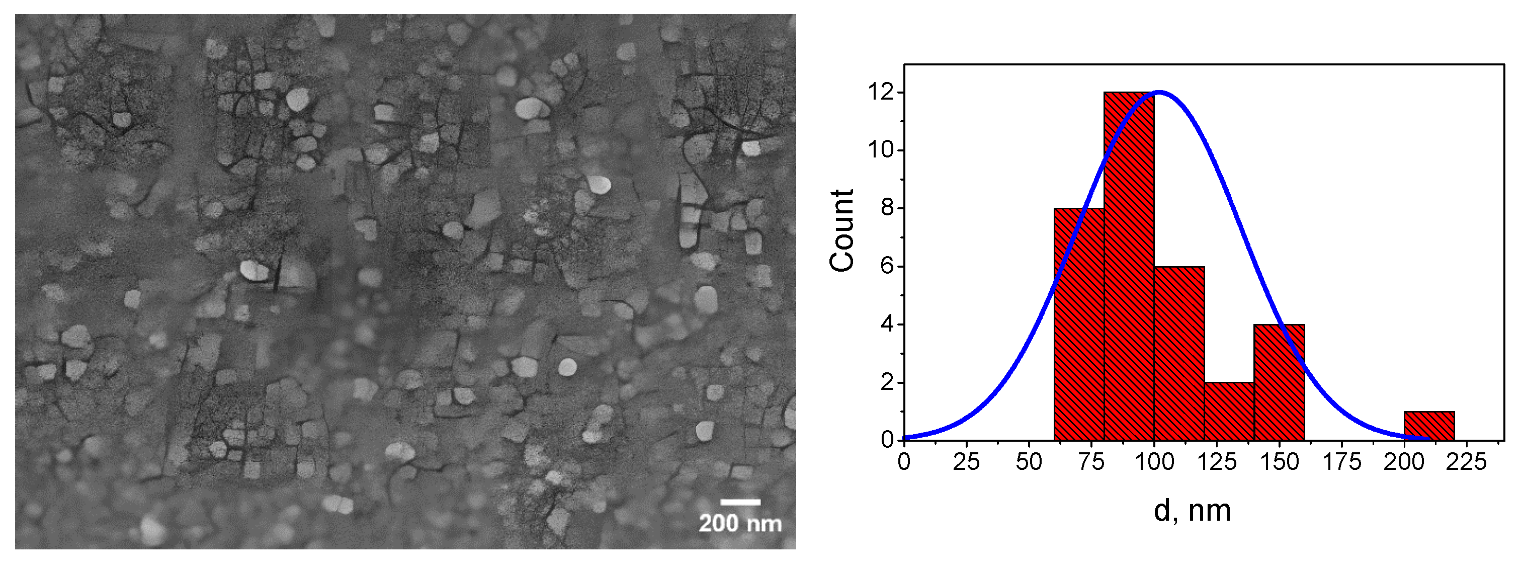
The surface morphology of both doped ZnO and ZnNiO thin films was examined by SEM. In Figure 2, we observed variations in the surface characteristics of the doped ZnO thin films compared to the Ni-doped ZnO thin films. The structure of undoped ZnO thin films was dominated by rod and grain structures. The structure of the thin ZnO film doped with 1% Ni showed an ordered morphology and grain and rod structure, while, with increasing Ni doping level, the thin structure of the ZnO film transformed into a porous and grain structure. The crystallite size and particle size are slightly different; there are differences in the values measured by XRD and SEM, respectively. This is explained by the fact that the calculation based on XRD peaks gives the crystallite size based on the Scherrer formula and not the particle size [25]. There can be several crystals with different misorientations in one particle. A dense vertically aligned network of hexagonal crystallites with an average diameter of 105 nm and an approximate height of 100 nm was observed, as shown in Figure 2. While the crystallites were not perfectly aligned, they showed a preference for vertical growth on the substrate and were distributed in a mostly uniform manner. This is also confirmed by the XRD data, in particular the value of the texture coefficient TC. The obtained aspect ratio (SAR) of 1.5–2, calculated from the length-to-diameter ratio of the rods, is in agreement with the values reported for the synthesized ZnNiO nanotubes [26].

3.3. Electrical Characteristics of the p-n Junction n-ZnO/p-Si

Our study involved measuring the electrophysical properties of heterostructures, particularly their current–voltage (I–V) curves. In addition, the I–V characteristics of the structures in the photoelectric mode, as well as the light characteristics of the heterostructures, were investigated. Measurements of the I–V characteristics were performed with a standard probe and an oscilloscope, employing the two-coordinate method. The temperature range was 20–200 °C. The radiation source was ultraviolet LEDs that emits light with a wavelength of λ = 365 nm and a power of 3 W (and LEDs that emit visible light).
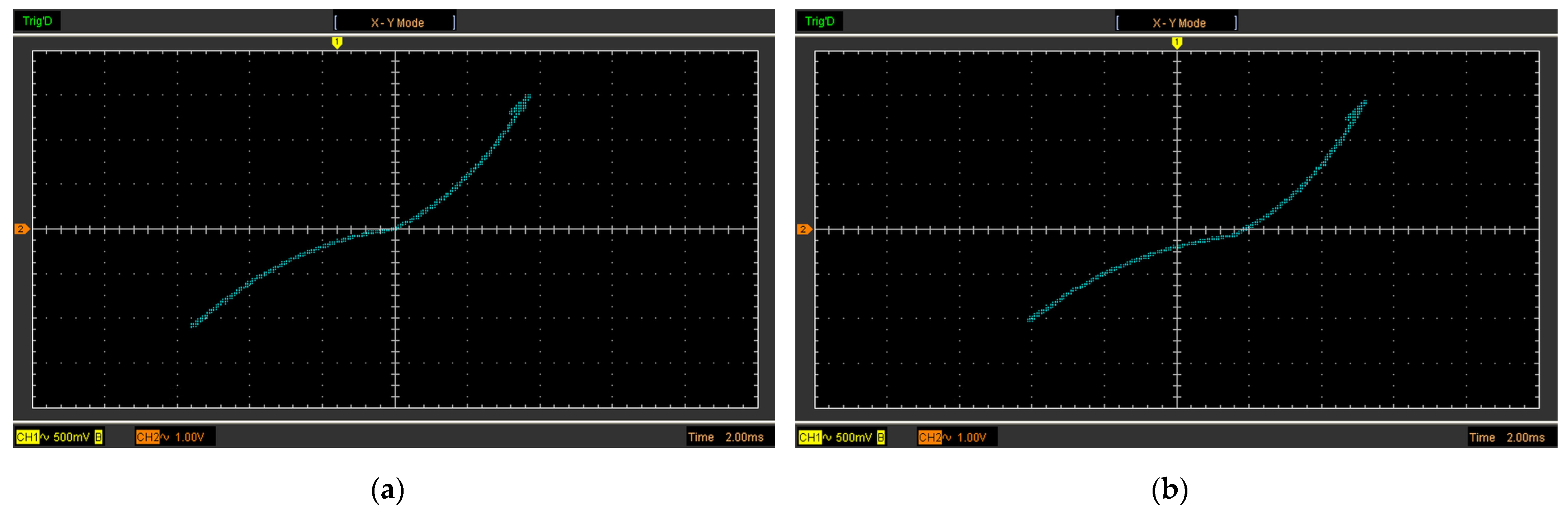
The active area of the heterostructure on the illumination side (film ZnO) was 2 × 2 mm2. With these dimensions and this deposition technology, the thin film was homogeneous. The correspondence of the composition of the films to the targets used in this technology, in particular when doping with transition metals, was shown in previous works [27,28]. The lower and upper silver ohmic contacts were obtained by applying a room-temperature silver paste to the substrate and working surface of the n-ZnNiO/p-Si heterostructures. The I–V behavior of the heterojunction was investigated over a voltage interval of −0.2 V to +0.2 V (Figure 3a,b). The nonlinear dependence between the applied voltage and the output current through the heterostructure can be expressed as follows using a relation of the following form:
V = I s · e q V n k T 1 ,
where I is the current strength, q is the electron charge, k is the Boltzmann constant, T is the absolute temperature and Is is defined as the reverse saturation current. The non-ideality factor n was determined by the slope of the logarithm (I) of the function V:
n = q k T · d V d ln I ,
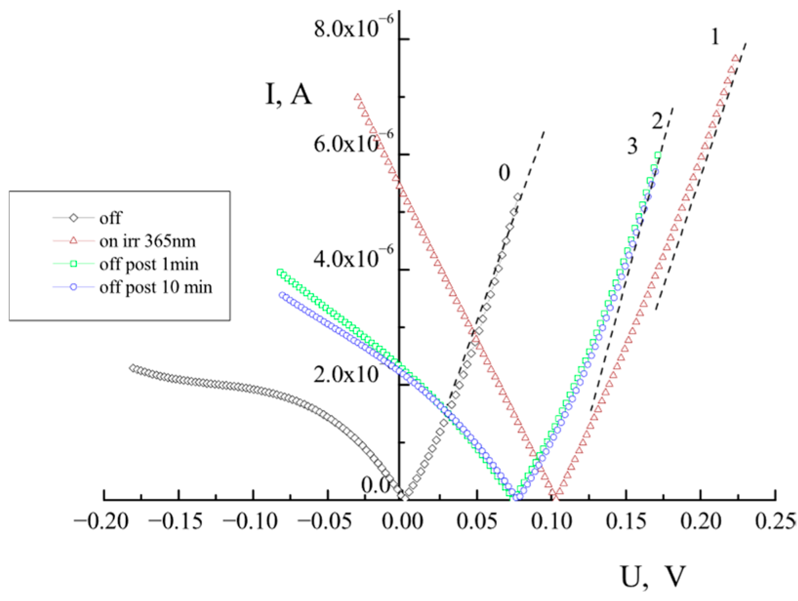
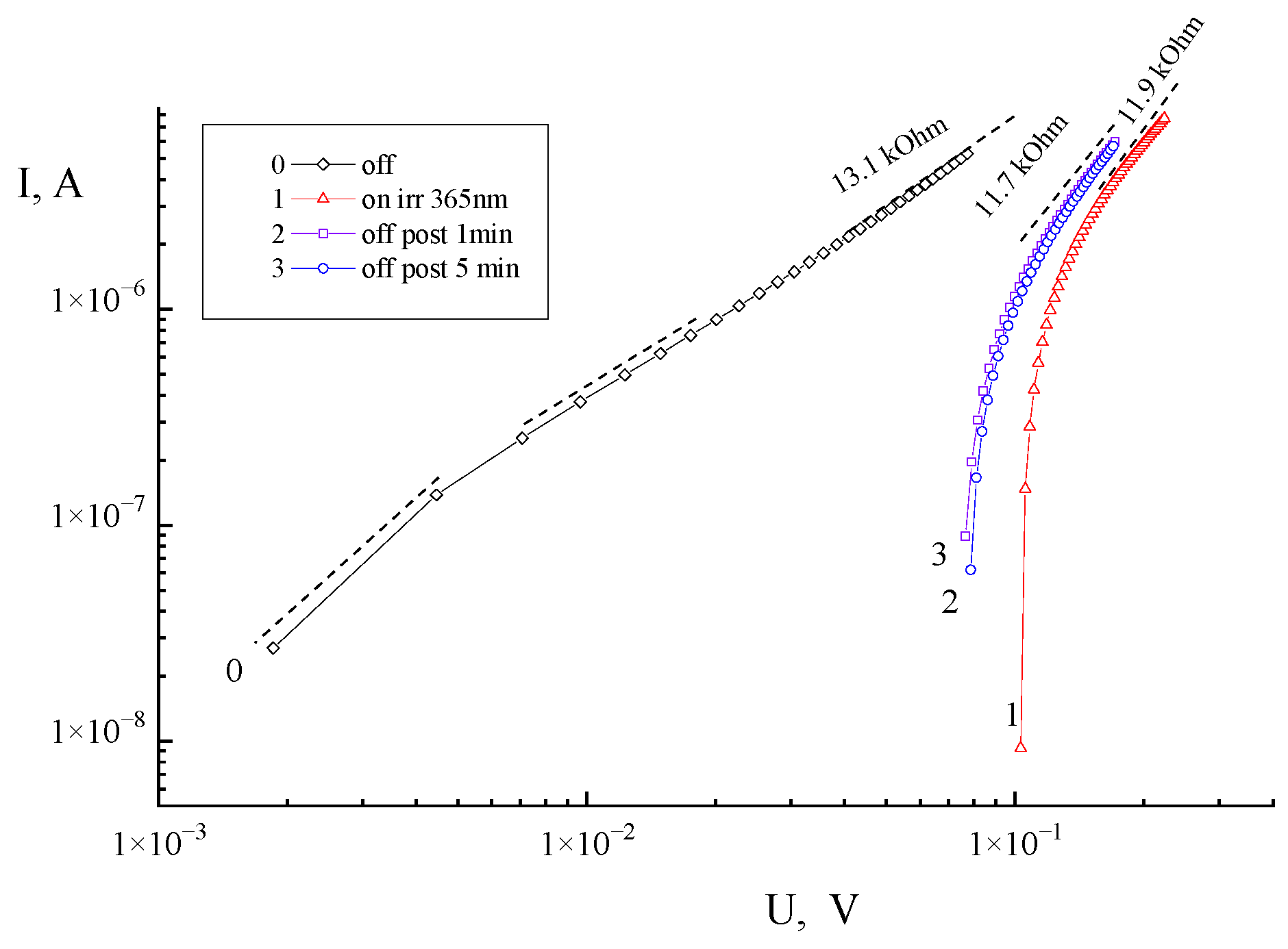
At constant voltage, an exponential increase in the measured current is observed in the forward direction. The results of the I–V measurements at room temperature are shown in Figure 4. The rectification coefficient (If/Ir, where If and Ir are the forward and reverse currents, respectively) in the dark was approximately 10 at ±0.2 V, which confirms the formation of a transition between n-ZnNiO and p-Si [29] (Figure 4).
The mechanism of electric charge transfer through the heterostructure can be observed on the branches of the I–V characteristic in the forward direction. For this, a logarithmic plot of the I–V characteristic of the structure without illumination is given [30]. All dependences of the current strength I on the voltage V are given in logarithmic coordinates. Figure 5 shows three regions. Three different regions are evident on the graph, and their appearance is determined by the applied transition voltage. This indicates different mechanisms of charge transport at the ZnNiO/Si interface [10,31,32].
At a very low forward voltage V < 0.01 V, nonlinear behavior is observed. In this type of wide-gap n-p heterostructure, the current increases according to a power law. This corresponds to an almost quadratic power law I(V) ~Vα, where (α ≈ 1.8), and the current flows through the tunneling recombination mechanism. An increase in the forward voltage leads to another charge-transport mechanism. Thus, the Ni-doped p-ZnNiO/n-Si heterojunction exhibits a rectifying I–V characteristic.
In the second region 0.01 < V < 0.02, an exponential behavior of the current Ι(V)~exp(δ∗V) is observed—where the parameter δ = 33.7. The exponent shown in Figure 5 suggests that the transport mechanism involves electron tunneling from the n-ZnNiO conduction band to interfacial states within the p-Si valence band. This process is completed by the recombination process.
In the third region, where V > 0.03, the current I exhibits a power law dependence on the applied voltage, following I(V) ≈ Vα with α ≈ 1.4. According to theory [33], this type of I–V characteristic arises from the combined effects of ambipolar diffusion and drift of non-equilibrium carriers during the modulation of charge carrier injection. The observed behavior implies that space-charge conduction is the dominant mechanism for charge transport. The value δ, which governs the primary exponential characteristic, is determined by the donor concentration in the zinc oxide layer [32,34]. This holds under conditions where the acceptor concentration in silicon (NA) is approximately equal to the donor concentration in zinc oxide (ND):
δ 16 π 3 h · m e ε N D   ,
the effective mass of the electron is 0.27 m0. The symbol ε represents the permittivity of zinc oxide (ε = 8.9·ε0 [35]) and is Planck’s constant.
Based on Equation (7), the doping level of the thin layer n-ZnNiO can be estimated. This allows us to estimate the donor concentration in the layer as ND = 9.8 × 1018 cm−3. The high subsequent stability and low impurity concentration observed result from factors related to current bias conditions and a decrease in the rectification coefficient. The doping level in the layer determines the height of the interfacial energy barrier. This relationship is mathematically expressed as the ratio of the saturation current to the height of the energy barrier at the interface. The reverse saturation current Is depends on the height of the barrier at the heterostructure interface:
I s = A A T 2 · e q Φ b k T ,
here, Φb represents the height of the zero bias barrier, A is the diode contact area (approximately 0.01 cm2) and A* is the theoretical Richardson constant (for ZnO material A* = 32 A cm−2 K−2). At higher voltages (around 0.2 V), we consider the series resistance (Rs) of the structural material, which is primarily due to a high-resistance layer:
d V d ln I = n k T q   + I R s ,
The relationship between d V d ln I and current is illustrated in the graph presented in Figure 5. Through linear curve fitting, the slope of the resulting curve yielded the series resistance, and the ideality factor n was found at its intersection with the Y-axis. From Equation (9) in our case we have the following values: in the dark, the series resistance value Rs = 13 kΩ; after illumination, Rs is 11 kΩ. The obtained non-ideality factors are 1.0 and 1.2, respectively. The height of the zero bias barrier height Φb found in this work is slightly larger than the difference in the energy band between ZnO and p-Si, which is consistent with the predicted dependence.
Φ b = k T q · l n A A T 2 I s ,
The barrier height of the Ag/ZnNiO/p-Si/Ag heterojunction, calculated according to the above formulas, was 0.64 eV, while the ideality factor was determined to be roughly 1.0 to 1.2. Several factors can cause the ideality factor to deviate from unity, including high series resistance, barrier inhomogeneity, tunneling processes, or non-uniform carrier distribution at the interface [36,37].
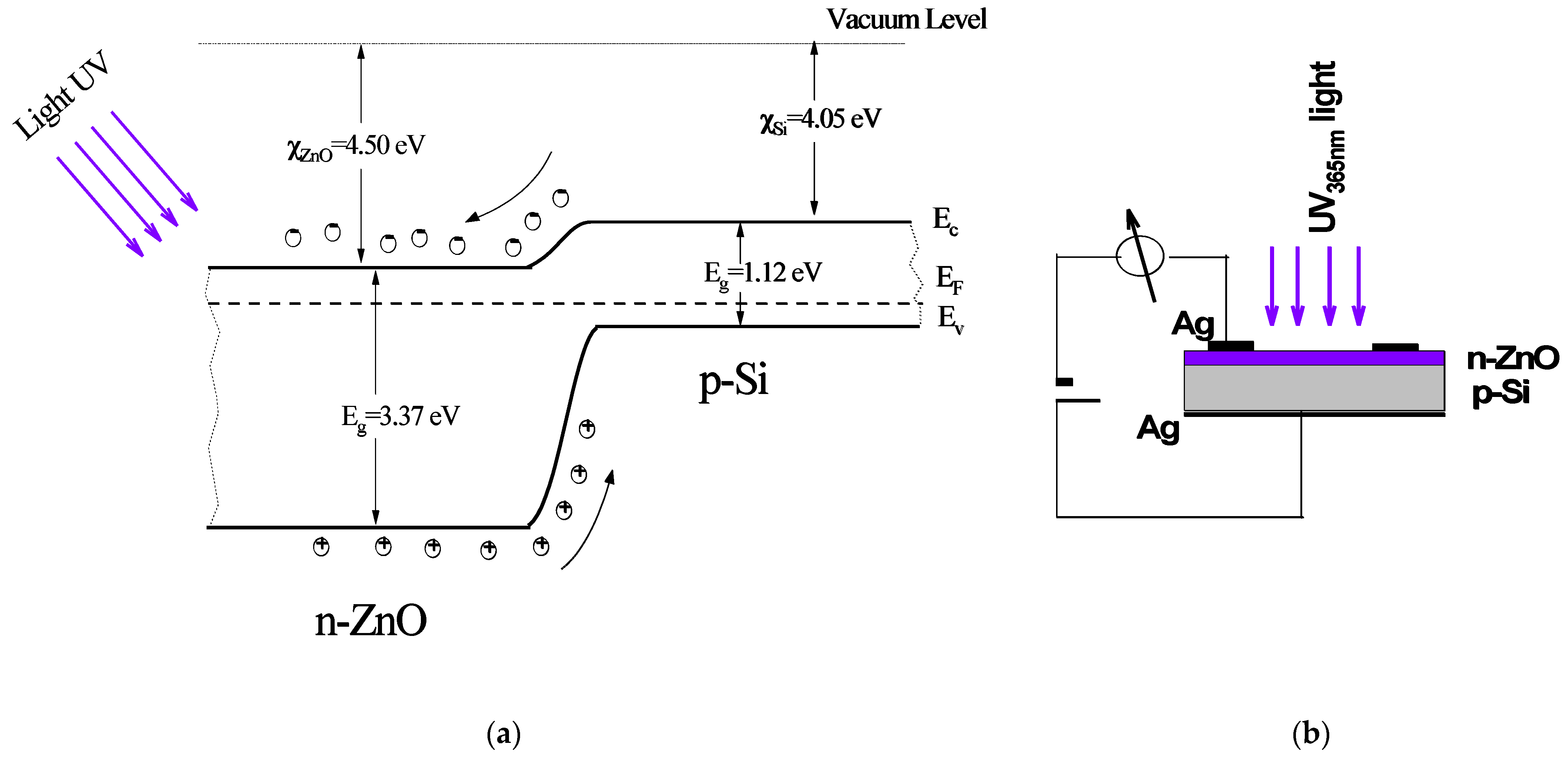
As a result, the magnitude of the conduction band (CB) offset between Si and ZnNiO governs the movement of charge carriers across the heterostructure [38,39]. For electronic applications, ZnO and Si materials are characterized by these energy structure parameters: ZnO = 3.36 eV, ZnO = 4.35 eV and Si = 4.05 eV, Si = 1.12 eV, respectively. As the carrier concentration of p-Si exceeds that in ZnO, the depletion region mainly forms within the ZnO material.
The energy diagram of the heterostructure is presented in Figure 6. The current flow in the heterojunction is considered to be the dominant electron flow from n-ZnO. This allows for the explanation of the rectification behavior in p-n junctions according to the Anderson model [40]. When reverse biased, the current is insignificant, determining the high rectification coefficient of the resulting heterostructure. Typically, the conduction mechanism in p-n junctions is governed by the principles of thermionic emission. The interfacial layer at the ZnNiO-silicon substrate interface causes the charge transport to differ from the standard thermionic emission model.
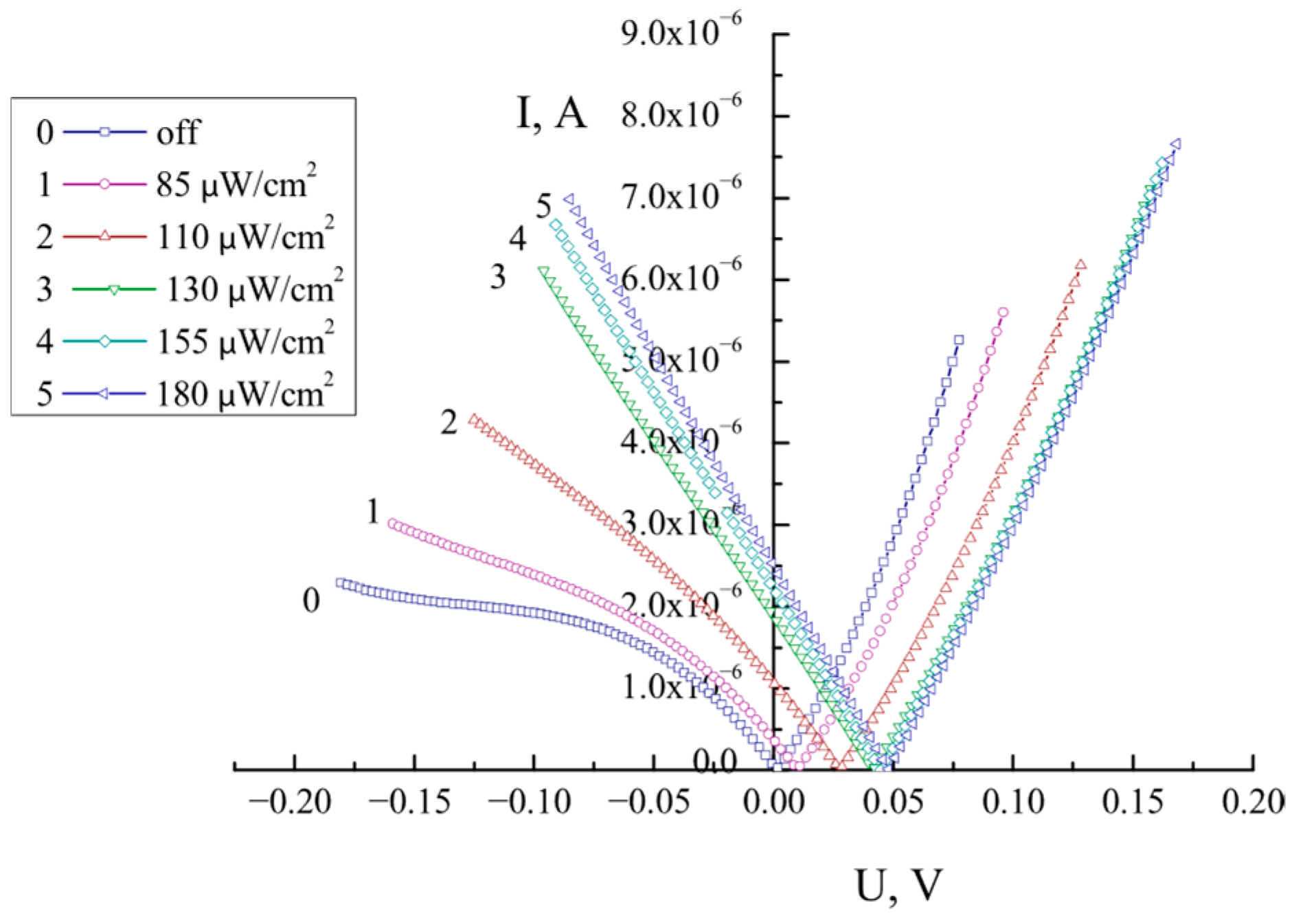
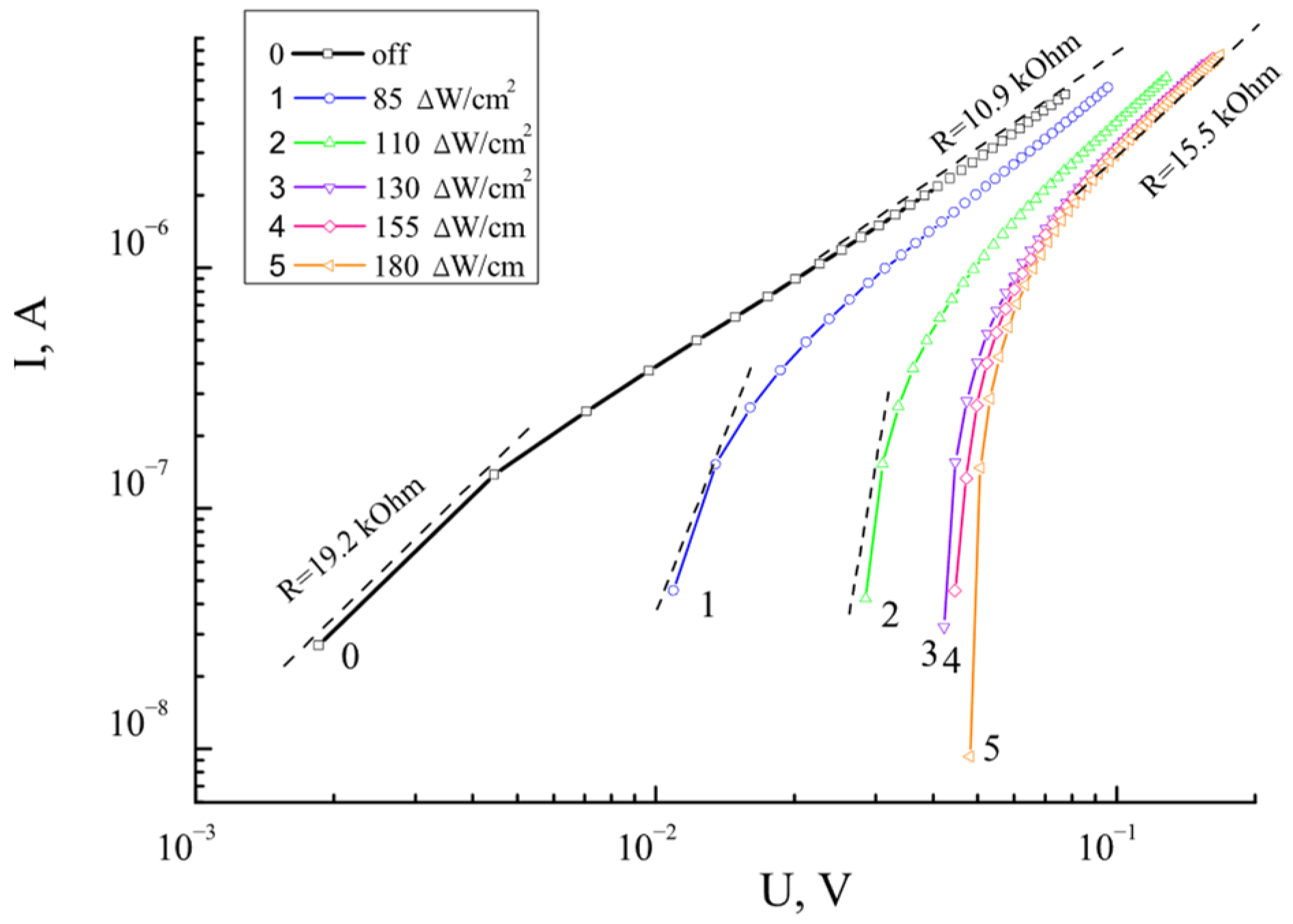
To determine how current flows in these structures when subjected to ultraviolet radiation, I–V characteristics were studied under 365 nm illumination with an intensity of E ranging from 0 to 0.2 mW/cm2 (Figure 7). The conductivity’s current–voltage characteristics for the n-ZnNiO/p-Si heterostructure at different illumination intensities are presented on a semi-logarithmic scale in Figure 8. These characteristics indicate nonlinear rectification behavior, where the open-circuit voltage depends on the intensity of the illumination.
It was observed that the open-circuit voltage of the heterostructures increased with greater illumination intensity when their light properties were examined. This can be explained by the comparatively large number of photons that excite valence electrons into the conduction band. The I–V characteristics of heterostructures show sublinear behavior under the influence of ultraviolet illumination and high-conductivity polarization. These regions can be approximated using the injection depletion effect. Secondary current carriers also play an important role in the operation of photodetectors. The I–V dependence can be explained by taking into account ambipolar diffusion and non-equilibrium carrier drift during carrier injection modulation. According to this theory, the forward bias region of the I–V curve is described by an analytical relation as follows:
I V = C · l n V V 0 ,
here, I represents the electric current value, V0 is the voltage at the onset of the superlinear region in the I–V characteristic, and C is a constant. When the thin film exhibits a substantial concentration of deep defects, this theory offers a satisfactory explanation. In this context, C is defined by Equation (12) [32]:
C = 2 d · A · q D p N t ,   D p = k T q · μ p ,
here, d is the cross-sectional thickness, and A is the surface area. Furthermore, the parameter C depends on the diffusion coefficient Dp of the main carriers (that is, their mobility μp), as well as the concentration of deep impurities Nt.
The mechanism of photosensitivity of the heterostructure can be explained as follows. In the dark, at zero voltage, oxygen molecules capture free electrons from the ZnNiO layer and adsorb on its surface in the form of negatively charged ions. A low electrical conductivity is formed near the surface of the ZnNiO layer. Exposure to ultraviolet light leads to the creation of electron-hole pairs, which in turn speeds up the movement of electric charges. As the intensity of ultraviolet light increases, more and more electrons receive enough energy to overcome the high barrier. With the application of reverse voltage, the barrier region expands and its height grows. In this scenario, the electric field created by the reverse bias reinforces the internal electric field.

3.4. Efficiency in Determining the Effect of Ultraviolet Radiation on the Si/ZnO p-n Junction

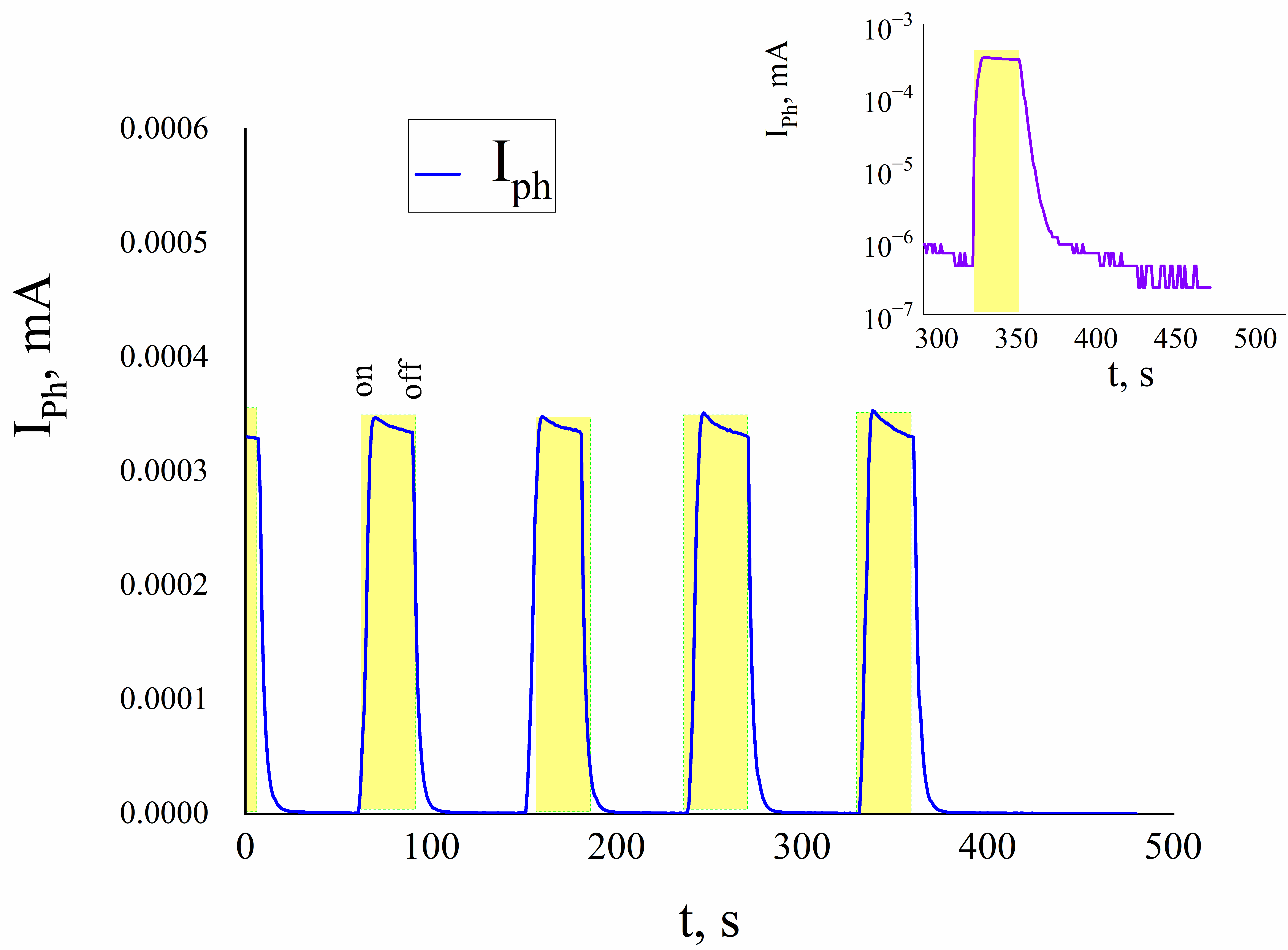
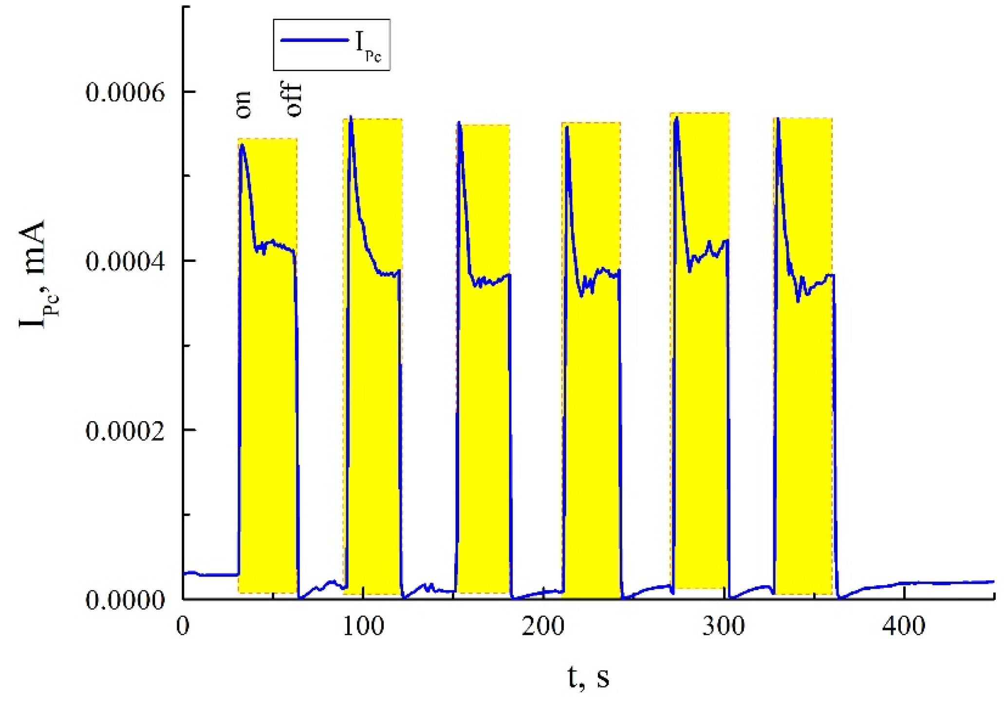
Under the action of ultraviolet irradiation at zero bias voltage, the photocurrent characteristics of the heterostructure were determined. The n-ZnNiO/p-Si sensor that we prepared showed a response (photosensitivity) to ultraviolet light. A fast response to ultraviolet light is demonstrated in Figure 9 when the UV LED was periodically activated and deactivated. The behavior of the photocurrent over time illustrates the repeatable and stable nature of the photosignal. Measurements of the dynamic characteristics of the radiation response were made with an oscilloscope. The rise time was from 2 to 1 s and the fall time was from 5 to 3 s. At high radiation intensity (about 0.2 mW/cm2) after illumination is turned on, the shape of the photosignal has sharp peaks that quickly disappear and the photosignal stabilizes (Figure 10).
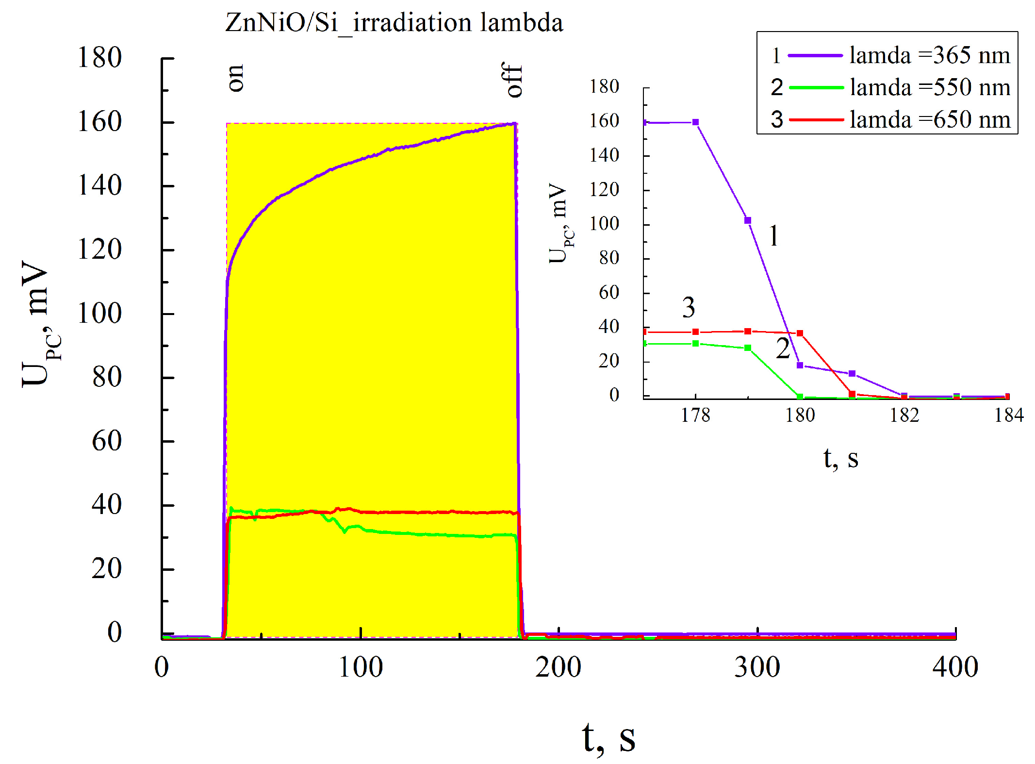
These peaks observed in photosignal time can be explained by the pyroelectric effect. The photoresponse peak is a rapid initial surge due to the nature of the pyroelectric phenomenon. This spontaneous electrical effect generates a pyroelectric signal in the volume of a thin ZnNiO layer under the action of ultraviolet light and superimposes it on the photoelectric signal [40]. This peak is clearly expressed at significant radiation intensities. The absorption of photons and the released energy correlate with the increase in temperature gradient (dT/dt) [41]. Clearly, by analyzing the appearance of the photoresponse curves at small and significant radiation intensities on the heterostructure, we can conclude that we are dealing with the total pyroelectric and photovoltaic effects. In practice, the heterostructure can be considered as a device with an autonomous power supply [42,43]. The electrical response shows that n-ZnNiO/p-Si heterostructures are potential candidates for modular devices with low power consumption and maximum photosensitivity in the UV region (Figure 11). Using the photosignal in the form of a photocurrent, the sensitivity of the heterostructure to radiation can be calculated by the following formula:
R λ A W = I P h P λ ,
where IPh is the net photocurrent (light current minus dark current) and Pλ is the power of the incident ultraviolet light at 365 nm. In this study, an ultraviolet sensitivity of approximately 205 mA/W was achieved at zero voltage (365 nm). We can compare the UV current photosensitivity results from this study with the published findings for ZnO/Si heterojunctions [44]. The sensitivity to ultraviolet radiation can also be slightly increased by modifying the structures of the p-n junctions by introducing interfacial layers. Taking into account the results obtained, mechanisms of UV photoconductivity of the heterostructure have been proposed [45]. The turn on of ultraviolet illumination leads to the formation of light-induced electron-hole pairs in the depleted ZnNiO layer [46,47]. As a consequence of illumination, the number of free carriers increases, and the depleted layer becomes narrower. The application of a reverse bias voltage to the junction causes these pairs to drift in the direction of the internal electric field. Consequently, the electric field will separate the electron-hole pairs, causing the electrons and holes to move toward the positive and negative electrodes of ZnNiO and Si, respectively. As a result, we observe an increase in both the carrier injection and the generated photocurrent. With an increase in the reverse bias voltage, the depletion region becomes wider, and this, in turn, enhances the intensity of the photocurrent produced by UV light. Conversely, under forward bias, photogenerated pairs form near the ZnNiO interface and drift towards the opposite polarity of the junction, resulting in an increased photocurrent. In the absence of an external voltage (when the junction acts as a self-powered device), the built-in electric field of the p-n junction is responsible for separating the carriers. Light-generated charge carriers move from regions where they are highly concentrated to regions where they are less concentrated, which in this case is from n-ZnNiO to p-Si.

4. Conclusions

Thin films of ZnNiO oriented along the c-axis (002) were grown on p-Si substrates by the pulsed laser deposition method at room temperature. The ZnO/p-Si structure with silver electrodes exhibits a remarkable response to ultraviolet light. We conducted an investigation into the photovoltaic properties of the heterostructure. The heterostructure responds to ultraviolet pulses even at zero bias voltage. The photocurrent of the Ag/ZnO/p-Si structure can reach 205 μA when irradiated with 365 nm UV radiation at 0.2 mW/cm2 and zero bias voltage. Changes in the intensity of ultraviolet radiation lead to variations in the width and height of the depletion layer barrier at the interface. These changes impact the transport of electrons and holes, thereby affecting the magnitude of the photogenerated current. This heterostructure also exhibits excellent stability and repeatability. The energy band diagram illustrates how the device responds to ultraviolet light under different bias conditions (zero, forward, and reverse). Our investigation of ZnNiO/p-Si heterostructures highlights their potential in optoelectronics.

Author Contributions

Conceptualization, I.V. and B.C.; Methodology, I.V., I.P., M.C., B.C. and P.P.; Validation, I.V., I.P., M.C., B.C. and P.P.; Formal analysis, I.V., I.P., M.C., B.C. and P.P.; Investigation, I.V., I.P., M.C., B.C. and P.P.; Data curation, I.V. and B.C.; Writing—original draft, I.V. and B.C.; Writing—review & editing, I.V. and B.C.; Visualization, I.V. and B.C.; Supervision, I.V. and B.C. All authors have read and agreed to the published version of the manuscript.

Funding

This research received no external funding.

Institutional Review Board Statement

Not applicable.

Informed Consent Statement

Not applicable.

Data Availability Statement

The raw data supporting the conclusions of this article will be made available by the authors on request.

Conflicts of Interest

The authors declare no conflict of interest.

References

  1. Cuadra, J.G.; Estrada, A.C.; Oliveira, C.; Abderrahim, L.A.; Porcar, S.; Fraga, D.; Trindade, T.; Seabra, M.P.; Labrincha, J.; Carda, J.B. Functional Properties of Transparent ZnO Thin Films Synthetized by Using Spray Pyrolysis for Environmental and Biomedical Applications. Ceram. Int. 2023, 49, 32779–32788. [Google Scholar] [CrossRef] [Scilit]
  2. Kołodziejczak-Radzimska, A.; Jesionowski, T. Zinc Oxide—From Synthesis to Application: A Review. Materials 2014, 7, 2833–2881. [Google Scholar] [CrossRef] [Scilit]
  3. Korotcenkov, G. Nanostructured Zinc Oxide: Synthesis, Properties and Applications; Awasthi, K., Ed.; Metal Oxid.; Elsevier: Amsterdam, The Netherlands, 2021. [Google Scholar]
  4. Suchikova, Y.; Nazarovets, S.; Konuhova, M.; Popov, A.I. Binary Oxide Ceramics (TiO2, ZnO, Al2O3, SiO2, CeO2, Fe2O3, and WO3) for Solar Cell Applications: A Comparative and Bibliometric Analysis. Ceramics 2025, 8, 119. [Google Scholar] [CrossRef] [Scilit]
  5. Srikant, V.; Clarke, D.R. On the Optical Band Gap of Zinc Oxide. J. Appl. Phys. 1998, 83, 5447–5451. [Google Scholar] [CrossRef] [Scilit]
  6. Pedra, T.K.; Carvalho, R.D.; Fernandes, C.D.; Gularte, L.T.; Jauris, C.F.d.M.; Moreira, E.C.; Ferrer, M.M.; Raubach, C.W.; Cava, S.d.S.; Jardim, P.L.G.; et al. Physical and Chemical Approaches of Photovoltaic Parameters in Dye-Sensitized Solar Cells to ZnO/ZnS:RGO-Based Photoelectrodes. Appl. Sci. 2024, 15, 291. [Google Scholar] [CrossRef] [Scilit]
  7. Tong, C.; Kumar, M.; Yun, J.-H.; Kim, J.; Kim, S.J. High-Quality ITO/Al-ZnO/n-Si Heterostructures with Junction Engineering for Improved Photovoltaic Performance. Appl. Sci. 2020, 10, 5285. [Google Scholar] [CrossRef] [Scilit]
  8. Son, J. UV Detectors: Status and Prospects. In Proceedings of the UV and Higher Energy Photonics: From Materials to Applications 2018; Lérondel, G., Cho, Y.-H., Kawata, S., Eds.; SPIE: Bellingham, WA, USA, 2018; p. 15. [Google Scholar]
  9. Chen, H.; Liu, K.; Hu, L.; Al-Ghamdi, A.A.; Fang, X. New Concept Ultraviolet Photodetectors. Mater. Today 2015, 18, 493–502. [Google Scholar] [CrossRef] [Scilit]
  10. Faraz, S.M.; Shah, W.; Alvi, N.U.H.; Nur, O.; Wahab, Q.U. Electrical Characterization of Si/ZnO Nanorod PN Heterojunction Diode. Adv. Condens. Matter Phys. 2020, 2020, 6410573. [Google Scholar] [CrossRef] [Scilit]
  11. Seo, Y.S.; Oh, S.G. Controlling the Recombination of Electron-Hole Pairs by Changing the Shape of ZnO Nanorods via Sol-Gel Method Using Water and Their Enhanced Photocatalytic Properties. Korean J. Chem. Eng. 2019, 36, 2118–2124. [Google Scholar] [CrossRef] [Scilit]
  12. Borysiewicz, M.A. ZnO as a Functional Material, a Review. Crystals 2019, 9, 505. [Google Scholar] [CrossRef] [Scilit]
  13. Cieniek, B.; Stefaniuk, I.; Virt, I.; Gamernyk, R.V.; Rogalska, I. Zinc–Cobalt Oxide Thin Films: High Curie Temperature Studied by Electron Magnetic Resonance. Molecules 2022, 27, 8500. [Google Scholar] [CrossRef] [Scilit]
  14. Ayachi, M.; Ayad, F.; Djelloul, A.; Sali, S.; Anas, S.; Guezzoul, M.; Benharrat, L.; Zougar, L.; Kermadi, S. Investigation of Structural, Morphological, and Optical Properties of (Ni/Co, Fe/Co, and Fe/Ni) Co-Doped ZnO Thin Films Prepared by Sol-Gel Spin Coating Technique. J. Sol-Gel Sci. Technol. 2024, 110, 503–517. [Google Scholar] [CrossRef] [Scilit]
  15. Gartner, M.; Chelu, M.; Szekeres, A.; Petrik, P. Towards Advanced Materials: Functional Perspectives of Co-Doped ZnO Thin Films. Micromachines 2025, 16, 1179. [Google Scholar] [CrossRef] [Scilit] [PubMed]
  16. Sood, S.; Kumar, P.; Raina, I.; Misra, M.; Kaushal, S.; Gaur, J.; Kumar, S.; Singh, G. Enhancing Optoelectronic Performance Through Rare-Earth-Doped ZnO: Insights and Applications. Photonics 2025, 12, 454. [Google Scholar] [CrossRef] [Scilit]
  17. Salem, M.; Akir, S.; Massoudi, I.; Litaiem, Y.; Gaidi, M.; Khirouni, K. Enhanced Photoelectrochemical and Optical Performance of ZnO Films Tuned by Cr Doping. Appl. Phys. A Mater. Sci. Process. 2017, 123, 243. [Google Scholar] [CrossRef] [Scilit]
  18. Berra, S.; Mahroug, A.; Hamrit, S.; Ahmad Azmin, M.; Zoukel, A.; Berri, S.; Selmi, N. Experimental and DFT Study of Structural and Optical Properties of Ni-Doped ZnO Nanofiber Thin Films for Optoelectronic Applications. Opt. Mater. 2022, 134, 113188. [Google Scholar] [CrossRef] [Scilit]
  19. Salem, M.; Haouas, A.; Almohammedi, A.; Ghannam, H. Structural and Optoelectronic Properties of Ni-Doped ZnO-Based Thin Films Deposited by Co-Precipitation Spin-Coating Method. J. Electron. Mater. 2025, 54, 5822–5830. [Google Scholar] [CrossRef] [Scilit]
  20. Guo, X.C.; Hao, N.H.; Guo, D.Y.; Wu, Z.P.; An, Y.H.; Chu, X.L.; Li, L.H.; Li, P.G.; Lei, M.; Tang, W.H. β-Ga2O3/p-Si Heterojunction Solar-Blind Ultraviolet Photodetector with Enhanced Photoelectric Responsivity. J. Alloys Compd. 2016, 660, 136–140. [Google Scholar] [CrossRef] [Scilit]
  21. Han, D.; Zhu, S.; Liu, J.; Liu, K.; Yang, Y.; Hu, S.; Liu, N.; Ye, J.; Zhang, W. Comb-Shaped Emitter Engineered p-NiO/n-ZnGa2O4/p-Si Heterojunction Bipolar Transistor for High-Performance Solar-Blind Ultraviolet Photodetection. ACS Photonics 2025, 12, 4598–4607. [Google Scholar] [CrossRef] [Scilit]
  22. Çavdar, Ş.; Şahin, Y.; Turan, N.; Koralay, H.; Tuğluoğlu, N. Structural and Electrical Characterization of Cd-Doped ZnO Thin Films Produced on p-Type Si Substrate by SILAR Technique. J. Mater. Sci. Mater. Electron. 2023, 34, 1787. [Google Scholar] [CrossRef] [Scilit]
  23. Dejam, L.; Sabbaghzadeh, J.; Ghaderi, A.; Solaymani, S.; Matos, R.S.; Țălu, Ș.; da Fonseca Filho, H.D.; Sari, A.H.; Kiani, H.; Shayegan, A.H.S.; et al. Advanced Nano-Texture, Optical Bandgap, and Urbach Energy Analysis of NiO/Si Heterojunctions. Sci. Rep. 2023, 13, 6518. [Google Scholar] [CrossRef] [Scilit]
  24. Kaushik, V.; Bhardwaj, K.; Kumar, D.; Kumar, M.; Sharma, S.K. Effect of Various Processing Parameters on the Properties of ZnO Thin Films. Hybrid Adv. 2024, 7, 100295. [Google Scholar] [CrossRef] [Scilit]
  25. Słowik, G.; Gawryszuk-Rżysko, A.; Greluk, M.; Machocki, A. Estimation of Average Crystallites Size of Active Phase in Ceria-Supported Cobalt-Based Catalysts by Hydrogen Chemisorption vs TEM and XRD Methods. Catal. Lett. 2016, 146, 2173–2184. [Google Scholar] [CrossRef] [Scilit]
  26. Choi, H.-S.; Vaseem, M.; Kim, S.G.; Im, Y.-H.; Hahn, Y.-B. Growth of High Aspect Ratio ZnO Nanorods by Solution Process: Effect of Polyethyleneimine. J. Solid State Chem. 2012, 189, 25–31. [Google Scholar] [CrossRef] [Scilit]
  27. Virt, I.; Potera, P.; Gamernyk, R.; Cieniek, B. Structural and Optical Properties of Ni-Doped ZnO Thin Films as TCO Material, Fabricated by Pulsed Laser Deposition Method. Opt. Mater. 2024, 154, 115643. [Google Scholar] [CrossRef] [Scilit]
  28. Potera, P.; Virt, I.; Cieniek, B.; Wisz, G. Optical Properties of ZnO:TM (TM = Cr, Mn and Co) Layers Obtained by Pulsed Laser Deposition Technique. Ukr. J. Phys. Opt. 2019, 20, 143–150. [Google Scholar] [CrossRef] [Scilit]
  29. Bo, H.; Quan, M.Z.; Jing, X.; Lei, Z.; Sheng, Z.N.; Feng, L.; Cheng, S.; Ling, S.; Yue, Z.C.; Shan, Y.Z.; et al. Characterization of AZO/p-Si Heterojunction Prepared by DC Magnetron Sputtering. Mater. Sci. Semicond. Process. 2009, 12, 248–252. [Google Scholar] [CrossRef] [Scilit]
  30. Raship, N.A.; Tawil, S.N.M.; Nayan, N.; Ismail, K. Effect of Al Concentration on Structural, Optical and Electrical Properties of (Gd, Al) Co-Doped ZnO and Its n-ZnO/p-Si (1 0 0) Heterojunction Structures Prepared via Co-Sputtering Method. Materials 2023, 16, 2392. [Google Scholar] [CrossRef] [Scilit]
  31. Özkartal, A.; Noori, D.T. Effects of Thermal Annealing on the Characterization of P-NiO/n-GaAs Heterojunctions Produced by Thermal Evaporation. J. Mater. Sci. Mater. Electron. 2021, 32, 13462–13471. [Google Scholar] [CrossRef] [Scilit]
  32. Chen, T.; Liu, S.Y.; Xie, Q.; Detavernier, C.; Van Meirhaeghe, R.L.; Qu, X.P. The Effects of Deposition Temperature and Ambient on the Physical and Electrical Performance of DC-Sputtered n-ZnO/p-Si Heterojunction. Appl. Phys. A Mater. Sci. Process. 2010, 98, 357–365. [Google Scholar] [CrossRef] [Scilit]
  33. Edmonds, L.D. A Theoretical Analysis of the Role of Ambipolar Diffusion in Charge-Carrier Transport in a Quasi-Neutral Region under High Injection. IEEE Trans. Nucl. Sci. 2011, 58, 2459–2469. [Google Scholar] [CrossRef] [Scilit]
  34. Saw, K.G.; Tneh, S.S.; Yam, F.K.; Ng, S.S.; Hassan, Z. Determination of Acceptor Concentration, Depletion Width, Donor Level Movement and Sensitivity Factor of ZnO on Diamond Heterojunction under UV Illumination. PLoS ONE 2014, 9, e89348. [Google Scholar] [CrossRef] [Scilit]
  35. Kaur, D.; Bharti, A.; Sharma, T.; Madhu, C. Dielectric Properties of ZnO-Based Nanocomposites and Their Potential Applications. Int. J. Opt. 2021, 2021, 9950202. [Google Scholar] [CrossRef] [Scilit]
  36. Guo, D.Y.; Shi, H.Z.; Qian, Y.P.; Lv, M.; Li, P.G.; Su, Y.L.; Liu, Q.; Chen, K.; Wang, S.L.; Cui, C.; et al. Fabrication of β-Ga2O3/ZnO Heterojunction for Solar-Blind Deep Ultraviolet Photodetection. Semicond. Sci. Technol. 2017, 32, 03LT01. [Google Scholar] [CrossRef] [Scilit]
  37. Zhang, Y.; Yang, F.; Guo, Q.; Feng, X.; Duan, Y.; Guo, J.; Cheng, G.; Du, Z. The Self-Powered Photodetector of n-Si/n-ZnO Heterojunction with Enhanced Temperature Adaptability via Transient Current Response. J. Phys. D Appl. Phys. 2022, 55, 504004. [Google Scholar] [CrossRef] [Scilit]
  38. Chala, S.; Boumaraf, R.; Bouhdjar, A.F.; Bdirina, M.; Labed, M.; Taouririt, T.E.; Elbar, M.; Sengouga, N.; Yakuphanoğlu, F.; Rahmane, S.; et al. Synthesis and Characterization of ZnO Thin Film for Modeling the Effect of Its Defectson ZnO/Cu2O Solar Cell EQE. J. Nano- Electron. Phys. 2021, 13, 01009. [Google Scholar] [CrossRef] [Scilit]
  39. Sharma, S.; Periasamy, C. A Study on the Electrical Characteristic of N-ZnO/p-Si Heterojunction Diode Prepared by Vacuum Coating Technique. Superlattices Microstruct. 2014, 73, 12–21. [Google Scholar] [CrossRef] [Scilit]
  40. Rakhshani, A.E. Optoelectronic Properties of P-n and p-i-n Heterojunction Devices Prepared by Electrodeposition of n-ZnO on p-Si. J. Appl. Phys. 2010, 108, 094502. [Google Scholar] [CrossRef] [Scilit]
  41. Wang, Z.; Yu, R.; Pan, C.; Li, Z.; Yang, J.; Yi, F.; Wang, Z.L. Light-Induced Pyroelectric Effect as an Effective Approach for Ultrafast Ultraviolet Nanosensing. Nat. Commun. 2015, 6, 8401. [Google Scholar] [CrossRef] [Scilit] [PubMed]
  42. Lu, X.L.; Guo, X.B.; Su, F.C.; Qiu, W.H.; Su, Z.; Li, J.; Li, W.H.; Jiang, Y.P.; Tang, Z.H.; Tang, X.G. Photoelectric Characteristics of Al-Doped ZnO/p-Si Diode Prepared by Radio Frequency Magnetron Sputtering. J. Phys. D Appl. Phys. 2022, 55, 485101. [Google Scholar] [CrossRef] [Scilit]
  43. Nadtochiy, A.; Podolian, A.; Korotchenkov, O.; Oberemok, O.; Kosulya, O.; Romanyuk, B. Equivalent Circuit Model to Reach Complicated Surface Photovoltage Transient Shapes in ZnO Thin Films. J. Nano- Electron. Phys. 2024, 16, 02023. [Google Scholar] [CrossRef] [Scilit]
  44. Al-Hardan, N.H.; Mohd Rashid, M.M.; Abdul Aziz, A.; Ahmed, N.M. Low Power Consumption UV Sensor Based on N-ZnO/p-Si Junctions. J. Mater. Sci. Mater. Electron. 2019, 30, 19639–19646. [Google Scholar] [CrossRef] [Scilit]
  45. Zainabidinov, S.Z.; Boboev, A.Y.; Makhmudov, K.A.; Abduazimov, V.A. Photoelectric Properties of N-ZnO/p-Si Heterostructures. Appl. Sol. Energy 2021, 57, 475–479. [Google Scholar] [CrossRef] [Scilit]
  46. Koc, N.S.; Altintas, S.P.; Gokcen, M.; Dogruer, M.; Altug, C.; Varilci, A. Current-Voltage Characteristics of Nano Whisker ZnO/Si Heterojunction under UV Exposition. Sens. Actuators A Phys. 2022, 342, 113618. [Google Scholar] [CrossRef] [Scilit]
  47. Dutta, M.; Basak, D. P-Zn O∕n—Si Heterojunction: Sol-Gel Fabrication, Photoresponse Properties, and Transport Mechanism. Appl. Phys. Lett. 2008, 92, 212112. [Google Scholar] [CrossRef] [Scilit]
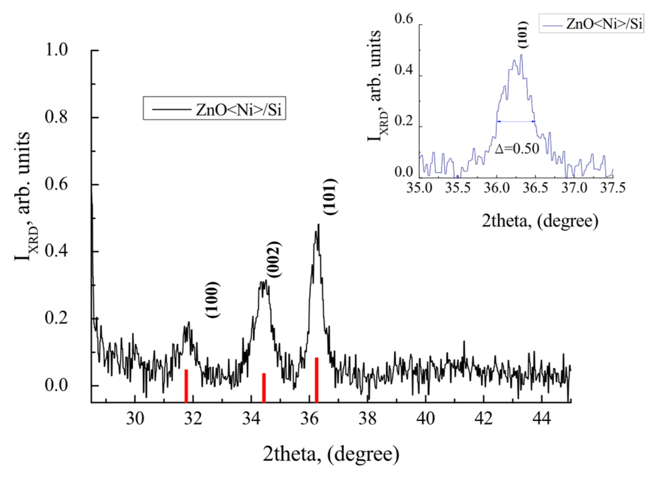
Figure 1. XRD diffractogram of Zn0.99Ni0.01O thin films. The inset shows an enlarged diffraction peak(101).
Applsci 16 02392 g001
Figure 2. SEM image of Zn0.99Ni0.01O thin film surface.
Applsci 16 02392 g002
Figure 3. Images of the current–voltage characteristic of the ZnNiO/Si heterostructure on the oscilloscope screen: (a) image in the dark, (b) under UV irradiation 0.2 mW/cm2.
Applsci 16 02392 g003
Figure 4. I–V characteristic of the ZnNiO/Si heterostructure: (0) in the dark, (1) during illumination with UV radiation, (2) 1 min after turning off the lighting, and (3) 10 min after turning off the lighting.
Applsci 16 02392 g004
Figure 5. Logarithmic graphs of the straight branches of the current–voltage characteristic of the ZnNiO/Si heterostructure: (0) in the dark, (1) during illumination with UV radiation, (2) 1 min after turning off the lighting, (3) 10 min after turning off the lighting.
Applsci 16 02392 g005
Figure 6. (a) Energy diagram of the n-ZnO/p-Si heterojunction; (b) scheme for measuring the photocurrent of a heterostructure.
Applsci 16 02392 g006
Figure 7. I–V characteristic of the ZnNiO/Si heterostructure depending on different intensities of illumination with UV radiation 0.0 ÷ 0.2 mW/cm2 with a wavelength of 365 nm.
Applsci 16 02392 g007
Figure 8. Logarithmic graphs of the straight branches of the current–voltage characteristic of the ZnNiO/Si heterostructure depending on different intensities of illumination with UV radiation 0.0 ÷ 0.2 mW/cm2 with a wavelength of 365 nm.
Applsci 16 02392 g008
Figure 9. Transient photocurrent characteristics for the fabricated ZnNiO/Si photodetector illuminated by UV light with an intensity of 0.16 mW/cm2 (at the exhibition on a semi-logarithmic scale).
Applsci 16 02392 g009
Figure 10. Transient photocurrent characteristics for the fabricated ZnNiO/Si photodetector illuminated by UV light with an intensity of 0.20 mW/cm2.
Applsci 16 02392 g010
Figure 11. Dependence of the sensitivity of the fabricated ZnNiO/Si photodetector on time when turning on and off illumination of different wavelengths of the same intensity (at the exhibition, on a semi-logarithmic scale).
Applsci 16 02392 g011
Table 1. Crystal structure parameters of the fabricated ZnNiO thin films.
(hkl) Planes2 θ (Degree)Intensity (arb.u.)dhkl (Å)FWHM (Degree)Dz
nm
TC
JCDPSObservedJCDPSObservedJCDPSObserved
(100)31.77031.81957422.81432.80900.558614.70.67
(002)34.42234.46144692.60332.59940.592814.01.43
(101)36.25336.2551001002.47592.47480.501616.70.99
Disclaimer/Publisher’s Note: The statements, opinions and data contained in all publications are solely those of the individual author(s) and contributor(s) and not of MDPI and/or the editor(s). MDPI and/or the editor(s) disclaim responsibility for any injury to people or property resulting from any ideas, methods, instructions or products referred to in the content.