Article

Multiscale Heat-Generation and Heat-Transfer Mechanisms and Coupling Effects in IGBT Modules

1
School of Energy and Power Engineering, Chongqing University, Chongqing 400044, China
2
Key Laboratory of Low-Grade Energy Utilization Technologies and Systems, Ministry of Education, Chongqing University, Chongqing 400044, China
*
Author to whom correspondence should be addressed.
Appl. Sci. 2026, 16(18), 9348; https://doi.org/10.3390/app16189348 (registering DOI)
Submission received: 15 August 2026 / Revised: 9 September 2026 / Accepted: 16 September 2026 / Published: 20 September 2026

Featured Application

The proposed computational framework supports physics-informed comparison of junction-temperature observables, cooling-boundary sensitivity analysis, and qualitative thermomechanical-risk screening for high-power-density IGBT converters.

Abstract

Insulated-gate bipolar transistor (IGBT) modules exhibit thermal behavior governed by interacting mechanisms spanning carrier transport, chip-scale diffusion, multilayer heat spreading, coolant convection, and thermomechanical response. This study presents an energy-consistent computational framework whose novelty lies not in the individual solvers, but in the explicit cross-scale energy interfaces, multirate synchronization, and observation operators that distinguish local-maximum, area-averaged, current-weighted, and sensor-related junction temperatures. Published first-principles and transport data for bulk silicon are used as reference-calibrated priors; the calculations implemented here comprise terminal-loss evaluation, prescribed energy-normalized spatial sources, analytical and two-dimensional diffusion reconstructions, three-dimensional finite-element thermal analysis, and a reduced-order Cauer network. For an 80 μm silicon chip at 400 K, the Fourier diffusion time is 0.12 ms, whereas the convention δT = 2√(αt) reaches the chip thickness at 0.030 ms; these values represent different diffusion criteria. In an illustrative boundary-sensitivity case, increasing h from 650 to 2000 W m−2 K−1 lowers the modeled maximum temperature from 132.1 to 99.6 °C without eliminating the central hotspot. The chip-side and cold-side cross-model differences are 1.28–2.98% and 9.54–12.56%, respectively, when terminal boundaries differ, while temperature-dependent loss raises the lumped Cauer peak by approximately 11 K. Mesh, time-step, and energy checks verify the numerical implementation, and cross-model comparisons assess consistency.

1. Introduction

Insulated-gate bipolar transistors (IGBTs) remain key switching devices in high-power motor drives, rail traction, renewable-energy conversion, and high-voltage power conditioning because they combine MOS-gate controllability with bipolar conductivity modulation. Increasing switching frequency, current density, and packaging compactness, however, produces large average losses, short-duration heat-flux peaks, and repeated thermal cycling. Heat generation is spatially and temporally nonuniform because conduction, turn-on and turn-off overlap, stored-charge extraction, free-wheeling-diode reverse recovery, and high-field events occur in different regions and on different time scales. The resulting junction-temperature level, temperature swing, and temperature gradient jointly affect electrical performance, protection margin, and package reliability. Recent reviews therefore identify junction-temperature acquisition, loss-to-temperature conversion, aging and lifetime prediction, and multiphysics thermal management as a coupled research problem rather than independent design tasks [1,2,3].
Current IGBT junction-temperature research can be grouped into direct measurement, temperature-sensitive electrical-parameter (TSEP) estimation, physics-based thermal modeling, and data-driven prediction. Direct optical or embedded-sensor methods provide valuable calibration and chip-level validation but are generally limited by packaging access, electrical isolation, bandwidth, or invasiveness. TSEP methods infer temperature from quantities such as the on-state collector–emitter voltage, switching-transition features, threshold-related signals, or the high-frequency response of an auxiliary component. They are attractive for online use, yet their accuracy depends on prior calibration, operating current, switching blanking, device aging, and the distinction between local-maximum and current-weighted mean temperature [4,5,6]. Chip-level and multi-condition methods have improved hotspot observability and adaptability under traction-inverter and double-sided-cooling conditions [7,8,9]. In parallel, Foster and Cauer networks, structure functions, thermal-impedance matrices, and compact multichip models remain the principal physics-based approaches. Recent studies have reduced online computational cost, compared Cauer-parameter extraction routes, included temperature-dependent material properties, and coupled neighboring chips through off-diagonal thermal paths [10,11,12]. Machine-learning models can further approximate nonlinear temperature maps, but their extrapolation and physical interpretability remain dependent on the coverage and quality of training data [13].
Research on IGBT loss and lifetime is increasingly organized as a mechanism chain from electrical loading to damage accumulation. Conduction loss is governed by the temperature- and current-dependent on-state voltage, whereas turn-on, turn-off, and reverse-recovery losses arise from voltage–current overlap, parasitic commutation, and the buildup or removal of stored charge. Modern loss models therefore use measured switching-energy surfaces or dynamic carrier-aware descriptions and feed the calculated loss back through the thermal model because rising temperature modifies mobility, lifetime, resistance, and switching energy [2,14]. Lifetime assessment then maps a mission profile to loss, junction-temperature history, cycle counting, and cumulative damage. The dominant package mechanisms are thermomechanical fatigue and creep caused by coefficient-of-thermal-expansion mismatch: bond-wire heel cracking or lift-off increases electrical resistance and current crowding, while die-attach and substrate-solder cracks, void evolution, and delamination increase thermal resistance and reduce the effective heat-transfer area. Aging-aware thermal control, recalibrated power-cycling lifetime models, high-gradient solder-fatigue studies, and electrothermal–mechanical simulations have improved the representation of these processes [15,16,17,18,19,20,21]. Nevertheless, many lifetime calculations still treat the temperature history as a prescribed input and do not close the feedback loop through which damage redistributes current and heat flow.
At the microscopic scale, IGBT heat generation is the irreversible transfer of carrier energy to the lattice. Electrons and holes accelerated by the local electric field lose momentum and energy through electron–phonon, impurity, defect, and interface scattering; recombination and high-field processes add further localized energy release. The same scattering physics determines mobility and carrier relaxation time and therefore changes both conduction loss and stored-charge dynamics. After energy enters the lattice, phonons are the principal heat carriers in crystalline silicon, and thermal conductivity follows from phonon heat capacity, group velocity, and scattering lifetime. Recent first-principles and Boltzmann-transport studies have improved phonon-limited carrier mobility and phonon-scattering-rate calculations, while spatially resolved measurements have quantified the strong reduction in silicon thermal conductivity produced by implantation damage and subsurface disorder [22,23,24]. These advances provide material functions and trends relevant to IGBT chips, but they are seldom transferred into device-scale dynamic heat sources and package-level thermal networks. Consequently, microscopic variables are often discussed qualitatively while continuum simulations continue to use constant conductivity, mobility, or uniformly distributed loss.
At the chip, package, and cooling scales, recent work has progressed from one-dimensional junction-to-case paths to temperature-dependent networks, three-dimensional heat spreading, multichip coupling, void-aware interfaces, and conjugate heat transfer models. Thermal-network studies show that mutual heating through shared DBC copper, ceramic, baseplate, and cooling structures requires coupling resistances or impedance matrices rather than independent Foster branches [11,12,25,26]. Heat-flow and finite-element models have also demonstrated that solder voids and interface degradation alter both the magnitude and spatial distribution of thermal resistance [27]. For inverter-level design, finite-element and flow-solid coupling analyses connect chip loss to package spreading, coolant-temperature rise, local convective coefficient, and pressure drop [3,28,29]. Recent pin-fin and microchannel studies further emphasize that cooling performance is spatially nonuniform and that reducing mean temperature alone does not necessarily eliminate central-chip hotspots or interphase thermal coupling [30,31]. However, the temperature observable supplied by these models is not always stated explicitly, and material, carrier, package, coolant, and damage models often exchange parameters without a common energy-consistent interface.
The literature thus provides mature tools at individual scales, but the interfaces among them often remain implicit. Three gaps are particularly relevant. First, local-maximum, area-averaged, current-weighted, and sensor-proximal junction temperatures are frequently compared without a common observation operator. Second, electrical energy is often transferred to continuum thermal models as a uniform source even when the pulse duration is shorter than the relevant diffusion time. Third, package damage is commonly evaluated after the thermal calculation rather than represented as a state that may alter electrical and thermal contact impedances. The unresolved problem is therefore not the absence of individual electrothermal or multiphysics solvers, but the absence of an energy-consistent and observable-consistent route for transferring their outputs across unequal time and length scales.
This study addresses these gaps through a hierarchical computational architecture linking first-principles-informed material descriptors, carrier-based loss mechanisms, chip diffusion, layered-package spreading, prescribed nonuniform cold-plate boundaries, thermomechanical-risk proxies, and reduced-order estimation. The contribution is the interface architecture rather than a claim that temperature-dependent properties, Cauer networks, finite-element analysis, or conjugate heat transfer are individually new. Specifically, the framework (i) conserves terminal loss when mapping it to spatial heat-source weights; (ii) preserves distinct observation operators for Tj,max, Tj,avg, Tj,J, and sensor-related temperatures; (iii) reconciles fast chip diffusion with slower package and cooling states through multirate exchange; (iv) separates numerical verification, cross-model comparison, and experimental validation; and (v) uses electrothermal loop gain to identify when sequential transfer is insufficient. These interfaces provide additional predictive discrimination between a true local hotspot, a lumped chip state, a boundary-condition mismatch, and a sensor-filtered temperature. The calculations implemented in this work are identified explicitly in Section 3, Section 6 and Section 7; published atomic-scale data and the full two-way CFD and calibrated damage/lifetime components are retained as framework inputs or future extensions rather than presented as a completed first-principles-to-module simulation chain.

2. Physical Hierarchy of the Multiscale Thermal Problem

Figure 1 presents the heat-generation and heat-transfer routes across the physical scales of an IGBT module, dividing the problem into atomic/electronic, carrier/device, chip/package, and cooling/system levels. Blue arrows denote the upward transfer of parameters and energy: microscopic band structure and scattering determine mobility and thermal conductivity; carrier motion generates spatial heat sources; the chip and package convert these sources into junction temperature and heat flow; and system boundaries determine the long-term thermal balance. Red arrows denote state feedback: temperature, strain, and defects modify material functions, whereas thermomechanical damage increases contact resistance and reduces the effective conducting cross-section, eventually producing current crowding and secondary hotspots. The multiscale problem is therefore not a series connection of four independent models, but a closed loop with scale-dependent time constants, spatial averaging operators, and feedback directions.
At the atomic scale, heat generation fundamentally arises from carrier scattering by the periodic lattice, impurities, and defects, followed by energy transfer to the phonon system. This scale does not directly output module thermal resistance; instead, it provides Eg, m*, εr, μ, and κ as functions of temperature, doping, and strain. At the carrier scale, the external terminal excitation is decomposed into channel electron injection, bipolar conductivity modulation in the drift region, recombination, impact ionization, and contact-region Joule dissipation, yielding q(x,y,z,t). Within the chip, this heat source first diffuses through the thickness and remains laterally nonuniform because of cell density, termination electric fields, and current crowding beneath bond-wire feet. In the package, heat spreads from the small chip area into larger copper layers. Highly conductive copper promotes lateral temperature equalization, whereas low-conductivity Al2O3 and solder interfaces support the principal temperature gradients. Multiple IGBTs and freewheeling diodes share the DBC, baseplate, and cold plate; hence both through-thickness and lateral coupling resistances are present. At system scale, heat crosses the thermal interface material into the cold plate and is removed by convection. Flow distribution, inlet temperature, and channel pressure drop make h(x,t) and Tf(x,t) spatially varying boundary fields. Short-time peaks are governed primarily by local heat-source density and the effective heat capacity of silicon; intermediate temperature swings by solder/DBC capacitance and spreading; and long-time mean temperature by the baseplate, interface material, and cold-plate boundary.
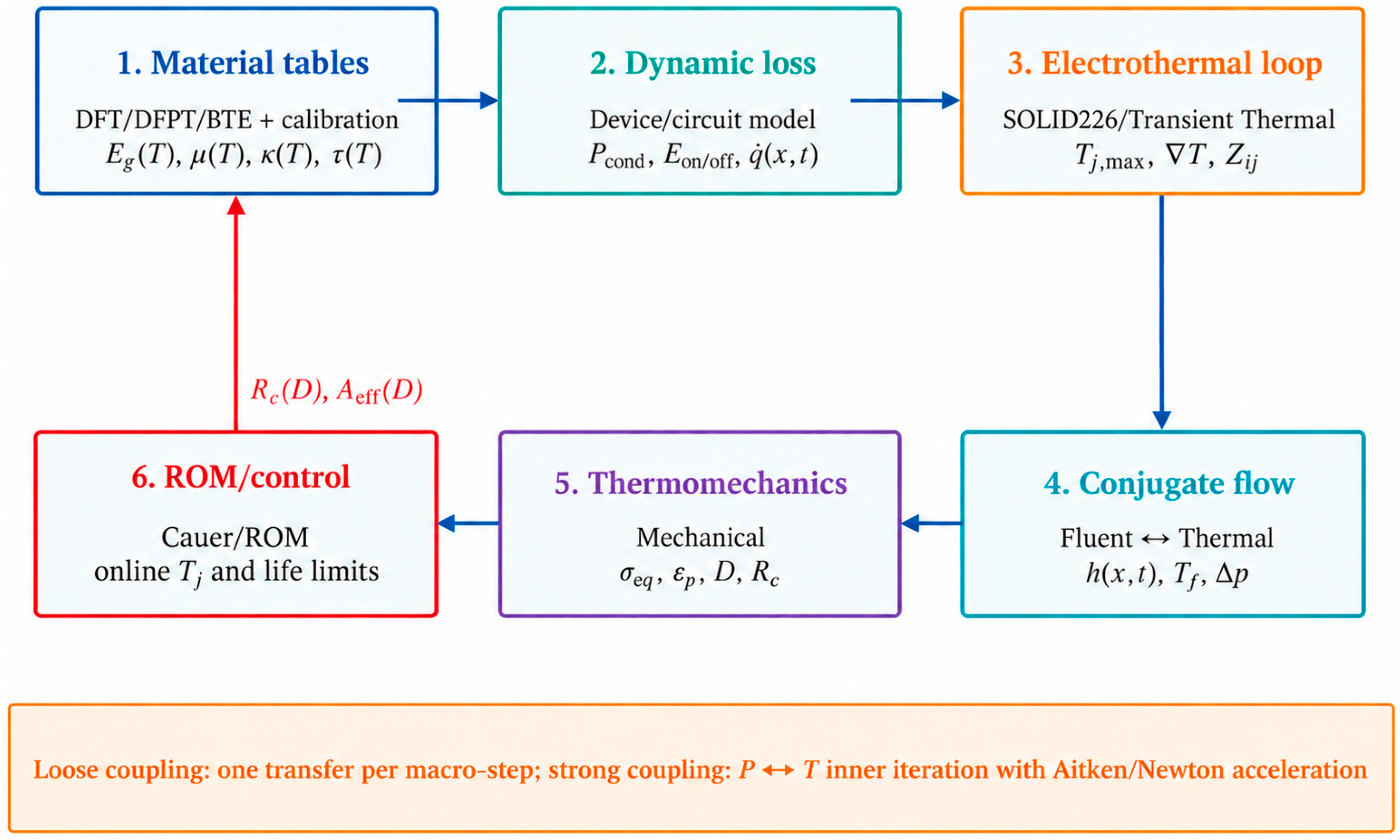
An asynchronous multirate solution is therefore adopted. Material response surfaces are updated offline; circuit/device models compute loss using ns-microsecond steps; the thermal model receives cycle-averaged heat sources at microsecond-to-0.1 s intervals; and fluid and damage variables are updated at slower macro time steps. Strong inner iterations within a macro step are invoked only when the temperature-loss loop gain approaches unity or when local avalanche or damage causes substantial current redistribution. This strategy preserves the dominant physics at each scale without imposing the switching frequency on the complete cold-plate mesh. Table 1 summarizes the key scales, state variables, and transfer interfaces. Importantly, the temperatures predicted or measured at different scales do not have identical spatial statistics. A device model generally requires instantaneous local junction-temperature feedback; infrared thermography is closer to the maximum surface temperature; a TSEP method often yields a current-weighted or area-averaged junction temperature; and an NTC network reflects the low-frequency temperature near the baseplate. Cross-scale comparisons must therefore define the spatial weighting and temporal bandwidth of the temperature observable before numerical agreement can be interpreted physically.
Four temperature observables are used consistently throughout this paper. Tj,max is the instantaneous maximum within the active junction region; Tj,avg is the uniform-area mean over that region; Tj,J is weighted by the local current density and approximates the quantity sensed by many temperature-sensitive electrical-parameter methods; and Tj,sens denotes the output of a specified sensor transfer function, including its spatial location and bandwidth. A baseplate negative-temperature-coefficient thermistor reading, TNTC, is therefore a sensor-proximal package temperature rather than a junction temperature. The unqualified symbol Tj is retained only for schematic or lumped reduced-order states whose weighting is stated in the accompanying text.

3. From First-Principles-Informed Parameters to Carrier Heat Generation

3.1. Atomic-Scale Material Parameters

At the atomic scale, this study uses published density functional theory, density-functional perturbation theory, and Boltzmann-transport results as external material priors rather than performing a new device-specific electronic-structure calculation. The temperature trends for band structure, phonon-limited mobility, scattering, and bulk-silicon thermal conductivity are synthesized from Refs. [22,23,24] and interpolated with the representative values in Table 2. Equations (1)–(4) define the physical provenance of these quantities and the interfaces required for a future device-specific calculation; they are not presented as the settings of an independently executed DFT/DFPT workflow. Accordingly, no exchange-correlation functional, pseudopotential, plane-wave cutoff, k-point mesh, q-point mesh, or supercell convergence result is claimed for the present study. Reproducibility of the calculations actually implemented here is instead specified by the material values in Table 2 and Table 3, the governing equations, the energy normalization in Section 3.2, and the mesh, time-step, boundary, and convergence criteria in Section 6. This distinction is necessary because ideal bulk-silicon priors cannot represent heavy doping, Si/SiO2 interfaces, metallization stress, irradiation damage, or process-induced defects without device-specific calibration [22,23,24].
ħ 2 2 / 2 m e + V e x t + V H n ] + V x c [ n ] ] ψ n k = ε n k ψ n k
E g T = E g 0 α V   T 2 / T + β V
κ α β T = V 1 Σ q v   ·   C q v T v q v , α v q v , β τ q v T
μ n , p T , N , ε = q τ e p h   v 2 / 3 k B   T F N N F E E F ε ε
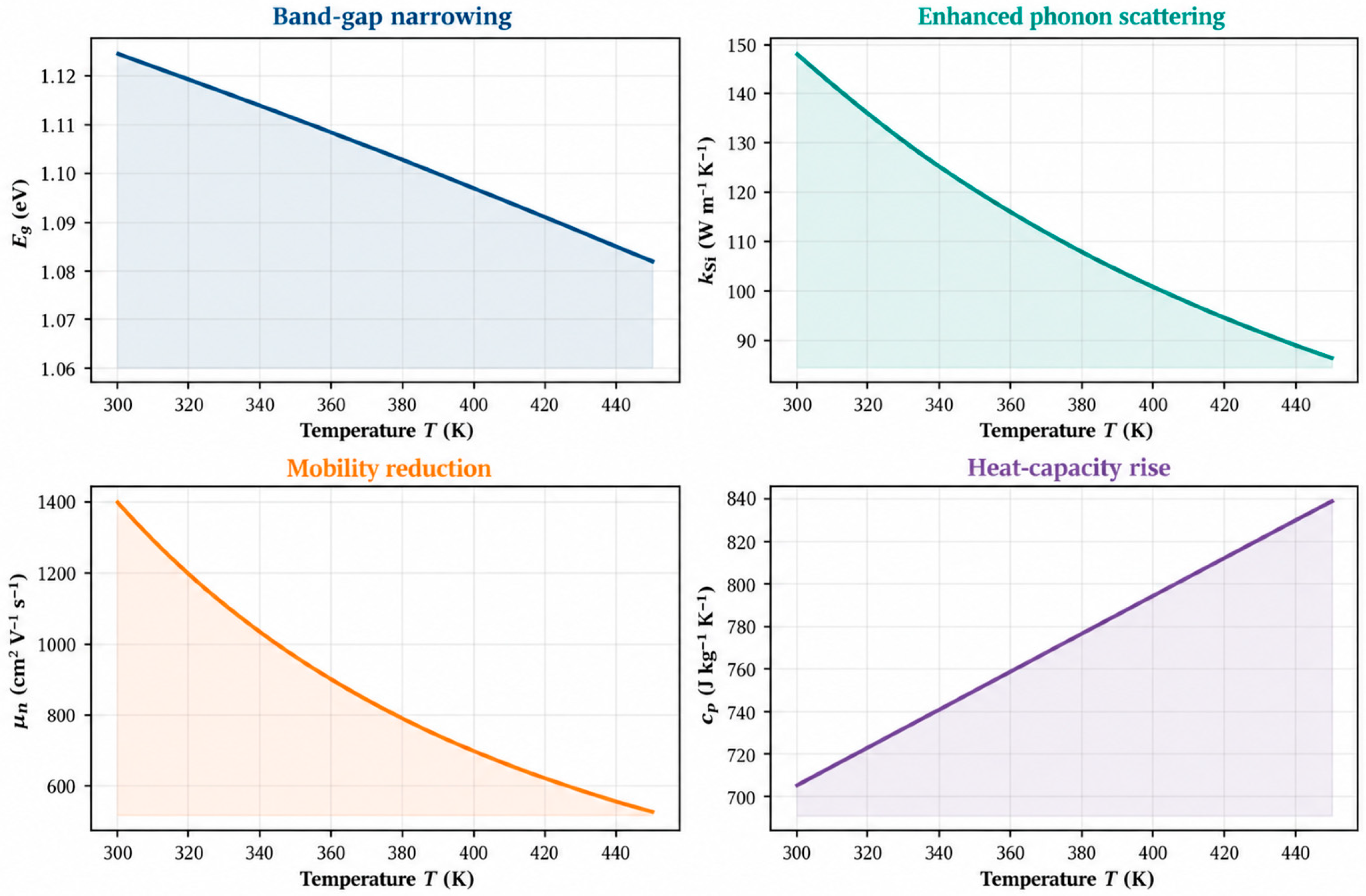
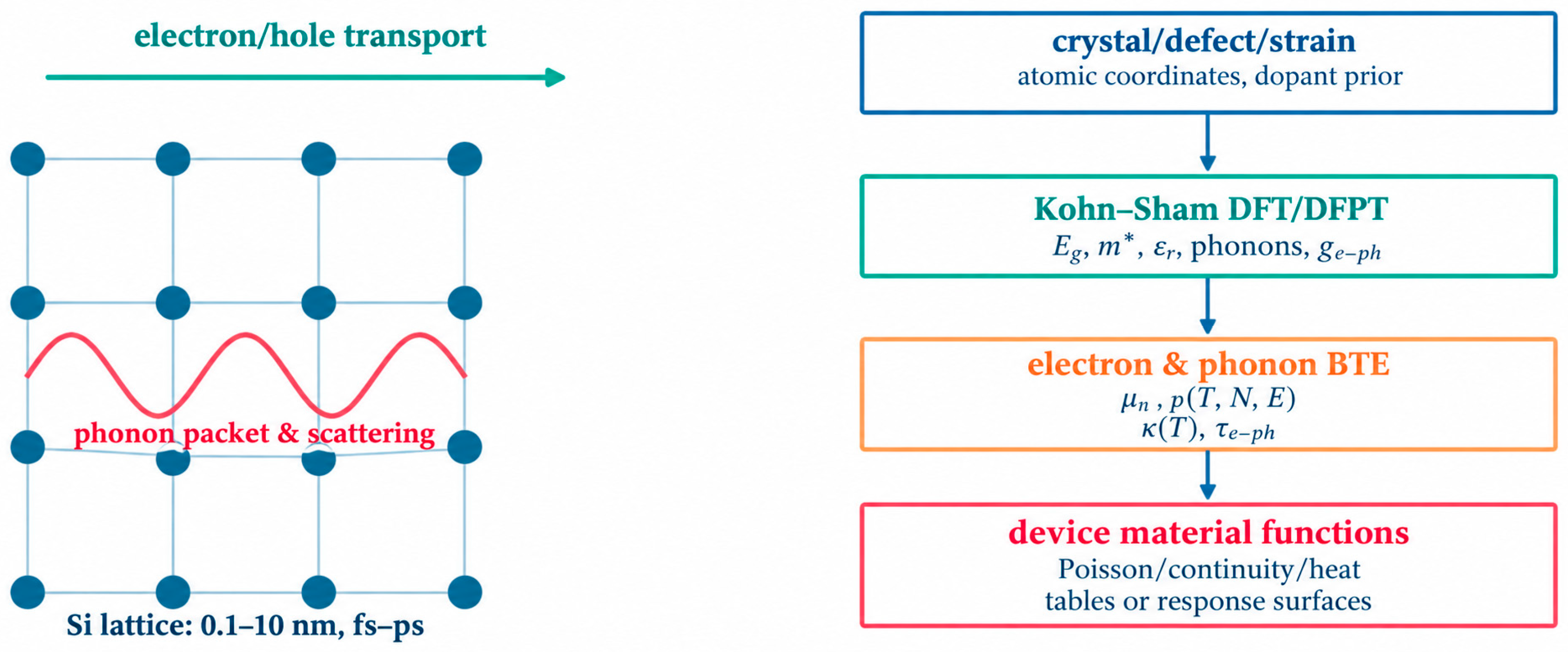
Figure 2 is calculated from reference-calibrated temperature-dependent functions synthesized from Refs. [22,23,24] and the bulk-silicon priors in Table 2; Figure 3 maps the corresponding first-principles-informed electronic and phonon descriptors to the continuum variables used in this work. Between 300 and 450 K, the Si bandgap, electron mobility, and thermal conductivity decrease, whereas specific heat increases. The consequences are not monotonic: reduced mobility raises channel and drift-region resistance, bandgap narrowing increases intrinsic carrier concentration and alters recombination, and carrier lifetime together with high-level injected charge controls the tail current. The temperature coefficient of loss therefore varies with current density and device structure and cannot be represented by a single constant αP. The lattice vibrations in Figure 3 represent phonon heat carriers, whereas the electron and hole arrows depict nonequilibrium transport driven by an external field. Band curvature controls effective mass; electron–phonon matrix elements and available phase space control scattering lifetime; and phonon group velocity and lifetime jointly determine κ. The resulting T-N-ε functions are reference-calibrated response surfaces, not unconditional material constants or direct measurements of the specific IGBT chip.
The effective masses and mobilities in Table 2 are reference-calibrated priors for bulk silicon rather than direct measurements or new device-specific first-principles outputs. The implemented thermal calculations use the thermal conductivity and specific heat listed in the material-property tables. At 400 K, for example, α = κ/(ρcp) = 98.9/(2330 × 794) ≈ 5.34 × 10⁻⁵ m2/s. This value is used consistently in the chip-diffusion calculations below; compared with 300 K, the lower diffusivity reduces penetration depth for the same pulse duration and increases the near-surface temperature rise.
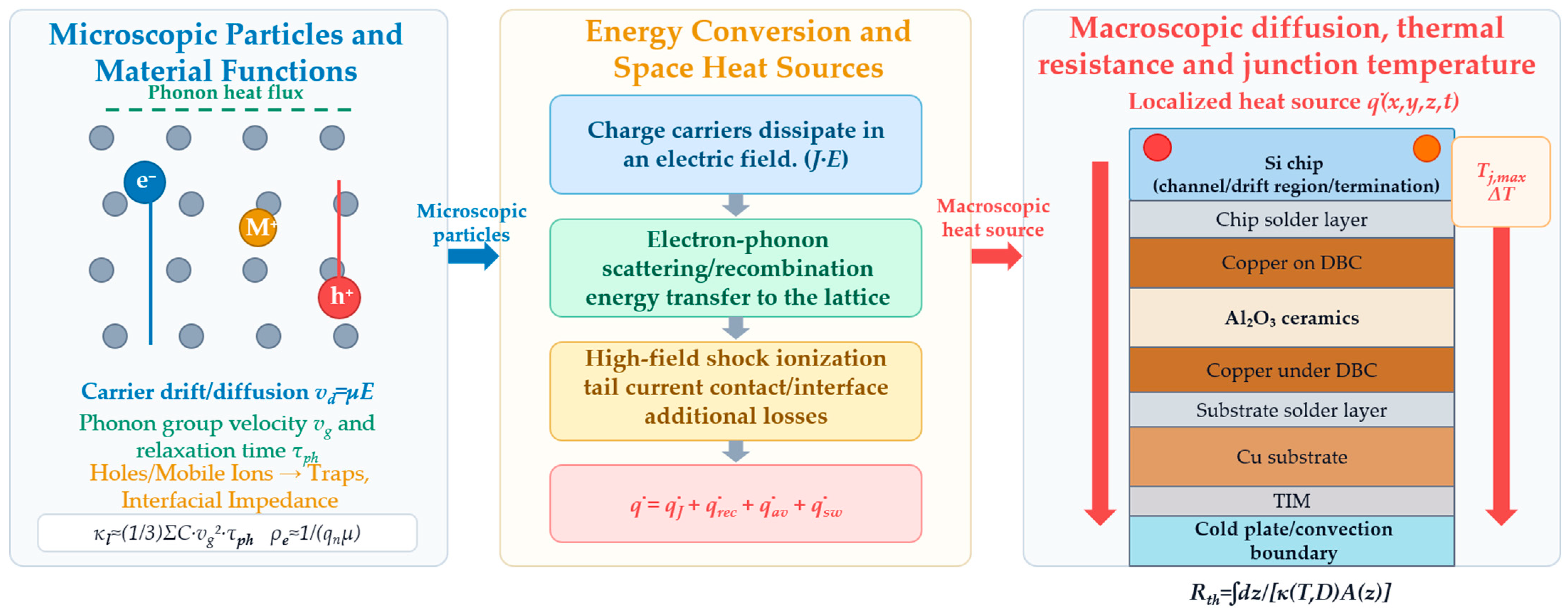
Using the carrier-energy and phonon-transport relations summarized in Refs. [14,21,22,23,24] together with the sample parameters in Table 2 and Table 3, Figure 4 shows how the macroscopic heat source used in a chip or package model is an upscaled consequence of microscopic nonequilibrium processes. In the conducting state, electrons injected through the MOS channel and holes injected from the collector drift and diffuse through the device under the local electric field. Their motion is repeatedly interrupted by electron–phonon, impurity, defect, and interface scattering. The field therefore performs irreversible work at the rate J·E, while carrier recombination and avalanche multiplication add localized source terms when the corresponding operating conditions are reached. During switching, creation and removal of stored plasma in the lightly doped drift region change both the spatial distribution and duration of heat generation. These microscopic events are not solved separately in the present thermal finite-element model; instead, they are volume- or surface-averaged into q · (x,y,z,t), with the averaging interval kept short relative to the relevant electrical transient and the integral constrained to equal the terminal loss.
The principal heat carriers in crystalline silicon are phonons. Once carrier energy is transferred to the lattice, the temperature field evolves according to phonon heat capacity, group velocity, and scattering lifetime, which together determine thermal conductivity and diffusivity. At the chip scale, the nonuniform source first establishes a steep near-junction gradient. The activated thermal mass then expands with diffusion length, while heat crosses the die attach, DBC copper, ceramic, baseplate, thermal interface material, and cold plate. Each layer spatially filters the original source: copper promotes lateral spreading, the ceramic produces a larger through-thickness drop, and imperfect interfaces add contact resistance. The resulting junction-temperature observables and associated temperature rises are therefore macroscopic state variables that retain information about microscopic loss, material functions, and package time constants. A single steady resistance cannot reproduce this chain when switching period, diffusion time, and coolant time scale are comparable.
The return arrow in Figure 4 is equally important. Rising temperature increases lattice vibration, shortens phonon and carrier relaxation times, reduces mobility and thermal conductivity, and modifies carrier lifetime. These changes alter conduction voltage, switching energy, tail-current duration, and thermal resistance, thereby feeding back into q · and the selected junction-temperature state. Strain, vacancies, interface traps, metallization degradation, and contact-area loss can further strengthen the loop by promoting current crowding or interfacial temperature jumps. In a crystalline-silicon IGBT, ordinary heat generation should not be interpreted as bulk ionic conduction of the type encountered in electrochemical cells. Ion or atom migration is instead most relevant as a slow aging variable associated with mobile contamination, vacancy transport, electromigration, and interface evolution. Consequently, a defensible multiscale model passes temperature-, field-, and damage-dependent response surfaces upward, then returns the calculated thermal and mechanical state to the microscopic or reduced-order material descriptions. This closed-loop interpretation provides the physical basis for the temperature and resistance trends introduced in the following sections.

3.2. Carrier Transport and Spatial Heat Sources

During IGBT conduction, the MOS channel injects electrons into the lightly doped n-type drift region while the p+ collector injects holes, producing conductivity modulation under high-level injection. Electrostatic potential and carrier densities are jointly constrained by Poisson’s equation and the continuity equations. The buildup and removal of the bipolar plasma in the drift region have finite time constants and cannot be replaced by a sequence of steady-state charge distributions. The potential and carrier fields satisfy [14,21]:
· ε φ = q p n + N D + N A
n / t = q 1 J n + G R   ;   p / t = q 1 J p + G R
J n = q μ n   n E + q D n n   ;   J p = q μ p   p E q D p p
Δ p / t = D a 2 Δ p / x 2 Δ p / τ H L + G i n j x , t
Equation (8) reveals the physical origin of the turn-off tail current. Gate turn-off interrupts the MOS channel but cannot instantaneously remove charge stored in the drift region. The carriers decay through recombination and extraction, causing current and voltage to overlap for a finite interval and generating substantial Eoff and local J·E dissipation. Increasing temperature reduces mobility and changes lifetime and intrinsic carrier concentration. The competing decrease in threshold voltage and increase in drift-region resistance make the temperature coefficient of VCE(sat) dependent on current density.
q · = J · E + q · r e c + q · a v + q · c o n t a c t Π J
V C E   I C + V G E   I G = Ω q · d Ω + d W f i e l d / d t + d W c h a r g e / d t + P r e t u r n  
P l o s s = D   V C E s a t I C + f s E o n + E o f f + E r r + P g a t e + P l e a k
Under high-level injection, the drift region may be further described by the ambipolar diffusion equation ∂Δp/∂t = Da2Δp/∂x2 − Δp/τHL. At turn-off, voltage recovers faster than stored charge is extracted, creating a loss interval in which high VCE coexists with tail current. Diode reverse recovery likewise generates localized high electric fields and recombination heat. The dynamic heat source must therefore represent irreversible dissipation rather than simply treating the full terminal product VCEIC as heat. Equations (9)–(11) provide a single-counting formulation for the dynamic heat source and energy.
In the parameterized calculations reported in Section 6 and Section 7, the spatial heat source is not exported from a full technology computer-aided-design device simulation. Total IGBT and diode powers are obtained from the terminal conduction, switching, and reverse-recovery loss relations, and these time-dependent powers are assigned to prescribed, energy-normalized spatial weighting functions tied to the chip footprints and local source scenarios. The normalization ensures that the volume integral of q · equals the corresponding device loss at each coupling step. The J·E, recombination, and avalanche terms above provide the physical basis and a route for future device-level coupling; the finite-element and equivalent-field cases in this study use prescribed equivalent distributions.
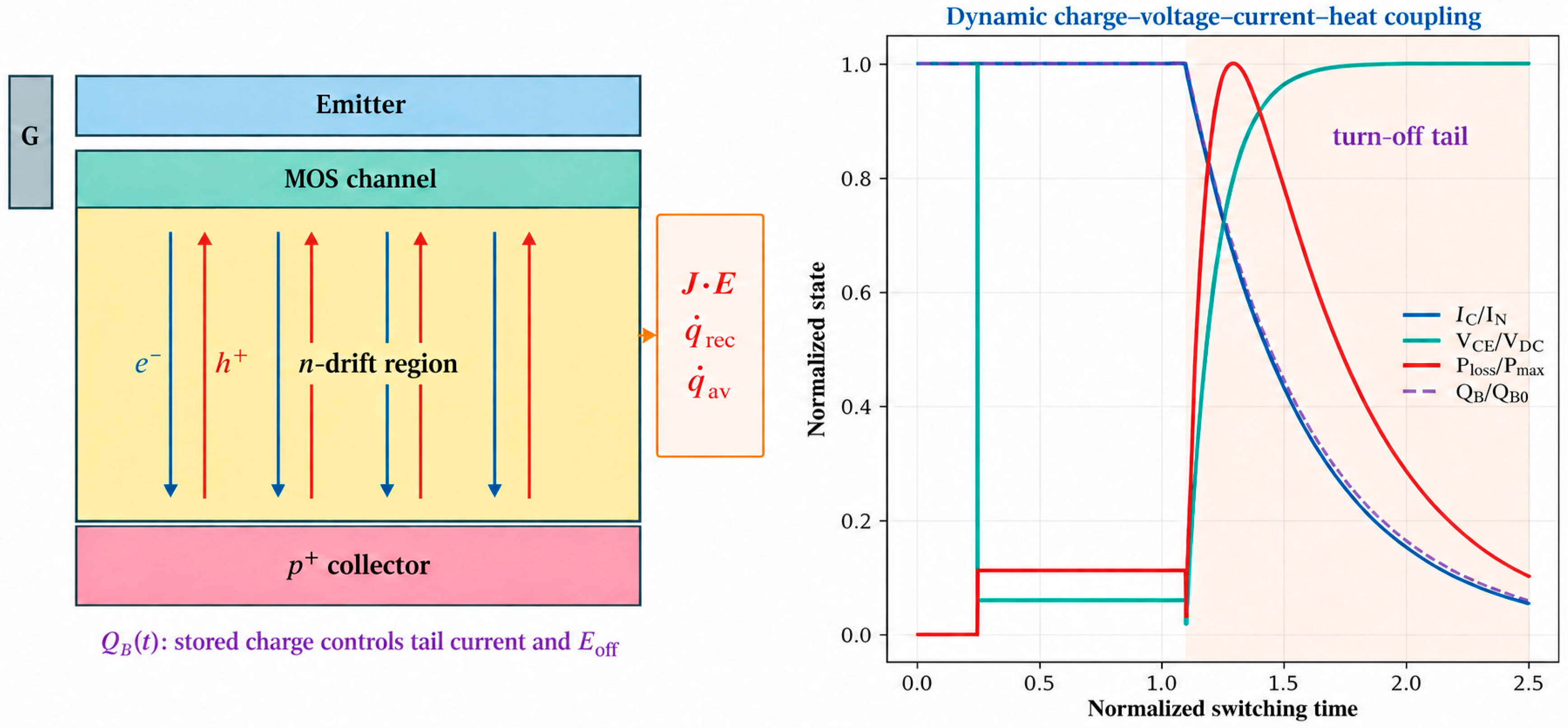
Figure 5 combines the carrier relations in Refs. [14,21] with normalized switching states for the sample IGBT. The left side shows counterflowing electron and hole injection and a J·E hotspot in the drift region; the right side shows that different heat-source components dominate during turn-on, steady conduction, and turn-off. When the gate voltage forms the MOS channel, electrons travel from the emitter into the lightly doped n-type drift region, while the p+ collector simultaneously injects holes. The drift region therefore contains both carrier types moving in opposite directions under the electric field. Injection of a large minority-carrier population increases the effective carrier concentration and lowers on-state resistance through conductivity modulation. This mechanism enables a low on-state voltage while retaining high blocking capability, but it also leaves substantial nonequilibrium charge in the drift region. QB(t) denotes the time-varying stored charge, approximated by Equation (12).
Q B ( t ) = q Ω d r i f t [ Δ n ( r , t ) + Δ p ( r , t ) ] d Ω ,
where q is the elementary charge, Δn and Δp are the excess electron and hole concentrations, respectively, and Ωdrift is the drift-region volume.
After turn-off, the MOS channel can disappear rapidly, but the stored charge in the drift region must decay gradually through carrier extraction, recombination, and transport to the external electrodes. The collector current therefore does not fall immediately to zero but develops a finite-duration tail. QB(t) is consequently the central state variable governing tail-current magnitude and duration and the turn-off energy Eoff. Volumetric heating within the device includes carrier Joule dissipation J·E, electron–hole recombination heat, and avalanche heating under high electric field. The right panel plots normalized collector current, collector–emitter voltage, instantaneous power loss, and stored charge through the switching transient. At the start of turn-off, VCE rises rapidly while IC remains appreciable, so their overlap drives Ploss = VCEIC to a peak. During the tail interval, the voltage is close to the dc-link voltage, but residual charge sustains a smaller current and continued loss. The amount and decay rate of stored drift-region charge thus control tail duration, turn-off energy, and transient junction-temperature rise. IGBT turn-off is inherently a multiphysics process coupling carrier transport, electric-field evolution, circuit response, and thermal effects. Stored charge is the bridge between internal carrier dynamics and external voltage, current, and heat-loss characteristics; tail current is its direct terminal manifestation and ultimately governs turn-off loss, transient temperature fluctuation, and thermal reliability.

4. Chip Structure, Package Heat Transfer, and System Cooling

4.1. Non-Quasi-Static Thermal Diffusion Within the Chip

The chip-temperature field satisfies the transient energy equation with temperature-dependent properties and a spatially varying heat source. Here, non-quasi-static does not imply failure of Fourier’s law; it means that the heat-source variation time is comparable to the internal diffusion time, so the temperature field cannot reach steady state at every electrical instant. For characteristic length Lc, the diffusion time is tau_d = Lc2/alpha and the Fourier number is Fo = αt/Lc2. The storage term partial T/∂t can be neglected only when Fo is much greater than unity, and the heat-source frequency is far below 1/τd [1,3,12].
ρ T c p T T / t = κ T T + q · x , y , z , t
F o = α t / L c 2 ; τ d = L c 2 / α ; q u a s i s t a t i c   o n l y   i f   F o 1
δ T t = 2 α t   ; Δ T r , t = 0 t Ω   G r r , t τ q · r , τ d Ω d τ
At 400 K, the thermal diffusivity of Si is α ≈ 5.34 × 10⁻⁵ m2/s. For an 80 μm chip thickness, the Fourier diffusion time τd = Lc2/α is 1.20 × 10⁻⁴ s, or 0.12 ms, corresponding to Fo = 1. Equation (15) uses the alternative characteristic penetration length δT = 2√(αt); setting δT = L gives t = L2/(4α) = 3.0 × 10⁻⁵ s, or 0.030 ms. The two values are therefore consistent but represent different criteria: τd is the order-one Fourier equilibration time, whereas δT = L marks penetration of the selected diffusion-length envelope across the thickness. For a 2–5 mm lateral cell or active-area scale, τd is approximately 0.075–0.47 s. When short-circuit, avalanche, or switching energy is deposited within 1–100 μs, the through-thickness Fourier number spans approximately 0.008–0.83 and is even smaller laterally. Heat consequently remains concentrated in the active region and near-surface layer during the earliest stage, making Tj,max sensitive to the prescribed spatial source; even after through-thickness penetration, the lateral hotspot remains non-quasi-static.
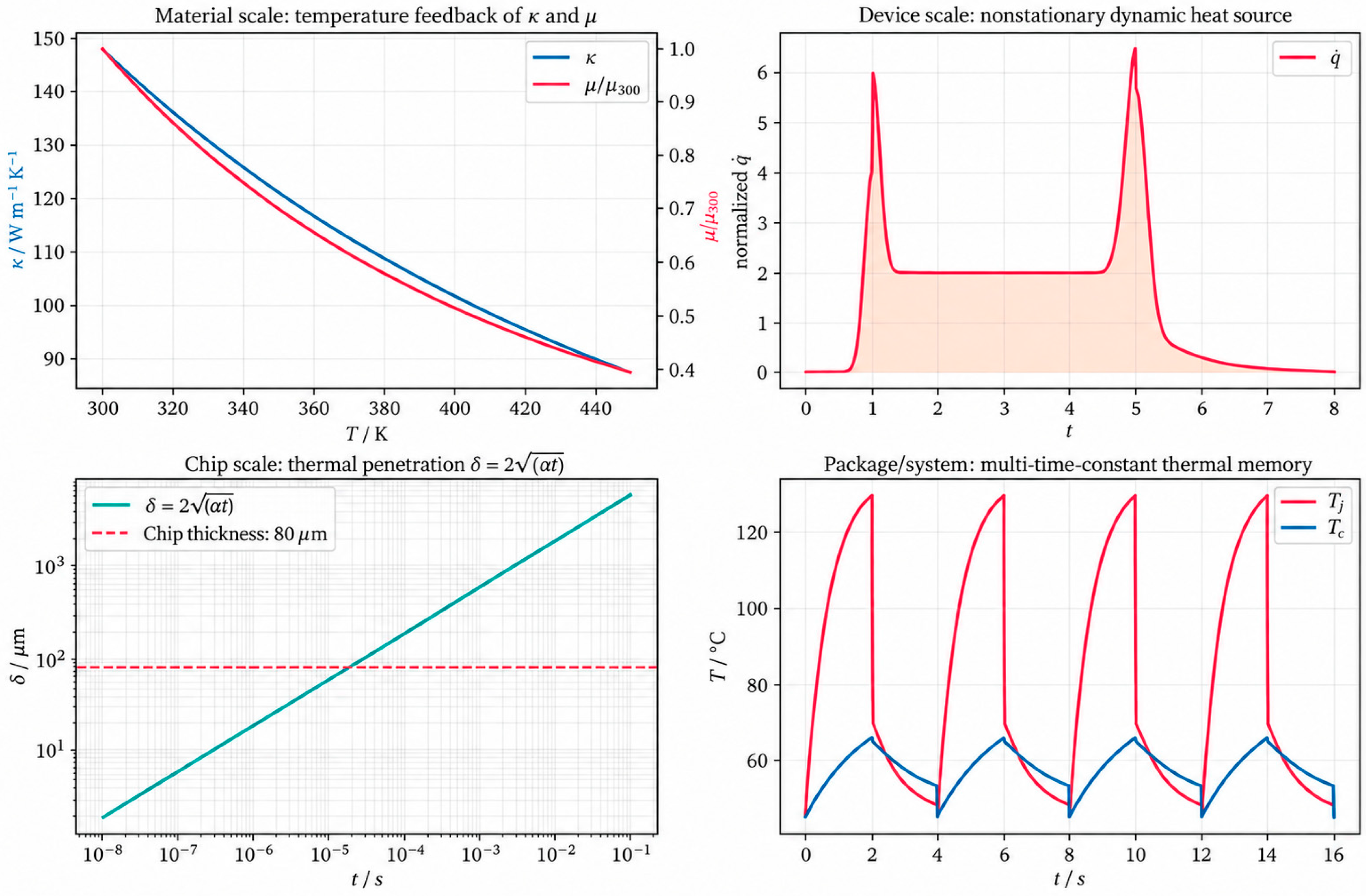
Figure 6 is a normalized multiscale calculation based on the temperature-dependent silicon data in Refs. [22,23,24], the carrier-loss trends in Ref. [14], and the sample thermal parameters in Table 2 and Table 3. It relates transient heat generation, cross-scale diffusion, and temperature response at the material, chip, device, and package/system levels. Power-device thermal behavior cannot be described as simple steady conduction; it is influenced jointly by temperature-dependent material parameters, dynamic loss fluctuations, evolving diffusion length, and multiple package time constants. The upper-left panel shows thermal conductivity κ and normalized carrier mobility μ/μ300 versus temperature. From 300 to 450 K, κ decreases from about 148 to 87 W m−1 K−1, while normalized mobility falls from 1.0 to about 0.4. Higher temperature intensifies lattice vibration and phonon scattering, shortening carrier mean free paths and reducing phonon transport efficiency. Lower thermal conductivity raises chip conduction resistance, whereas reduced mobility changes conduction characteristics and loss parameters. Constant-property analysis at high junction temperature may therefore underestimate temperature rise and local heat concentration within this computational model.
The upper-right panel illustrates the time evolution of the non-steady heat source at device level. The normalized volumetric source is initially near zero, rises rapidly to approximately six during the first transient, and decays to a quasi-steady level near two. During the second transient, it rises again to about 6.5 before decaying to zero. The waveform combines sustained conduction loss with transient switching loss. The quasi-steady plateau corresponds mainly to continuous conduction, whereas the peaks represent high instantaneous power caused by voltage–current overlap during turn-on, turn-off, or abrupt load changes. Although brief, these high-power-density peaks readily form local hotspots in the active region and influence the subsequent junction-temperature trajectory.
The lower-left panel uses the characteristic penetration length δT = 2√(αt) from Equation (15) to describe the expansion of the thermally affected region. With α = 5.34 × 10⁻⁵ m2/s at 400 K, δT reaches the 80 μm chip thickness at approximately 3.0 × 10⁻⁵ s. This penetration criterion is one-quarter of the Fourier time τd = L2/α = 1.20 × 10⁻⁴ s because the definitions differ by the factor of four stated explicitly above; it should not be interpreted as complete thermal equilibration. Below 0.030 ms, heat remains confined to the near-surface or local active region. At longer times, heat increasingly enters the die attach, copper cladding, ceramic, and baseplate, and interfacial resistance and package properties become dominant. Short-time models should therefore resolve nonuniform chip temperature, whereas longer-time analysis requires the multilayer package and external cooling boundary.
The lower-right panel shows the dynamic lumped junction-temperature state Tj,avg and the case temperature Tc under periodic power excitation. During an approximately 2 s loading interval, Tj,avg rises rapidly from about 45 to 130 °C, whereas Tc increases slowly to only about 66 °C. After the heat source is removed, Tj,avg falls rapidly, but Tc cools more gradually. Repeated loading leads to stable periodic oscillations. The faster response and larger swing of Tj,avg indicate small thermal time constants in the chip and nearby materials, whereas the smoother Tc trajectory reflects the larger effective heat capacity and longer time constants of the package, baseplate, and cooling structure. The substantial difference between their peaks confirms that case temperature alone cannot represent the transient chip state under rapidly varying operation.
In summary, the multiscale sequence proceeds from dynamic electrical loss to a local chip heat source, growth of the diffusion scale, interlayer package transfer, and dynamic junction- and case-temperature responses. Junction-temperature changes feed back through temperature-dependent thermal conductivity, carrier mobility, and related parameters to alter both loss and heat-transfer capability. Physically consistent computation under fast switching, periodic loads, and complex duty cycles therefore requires energy-normalized dynamic sources, temperature-dependent properties, chip-scale diffusion, and a package thermal network with multiple time constants; quantitative predictive accuracy still requires matched experimental validation.
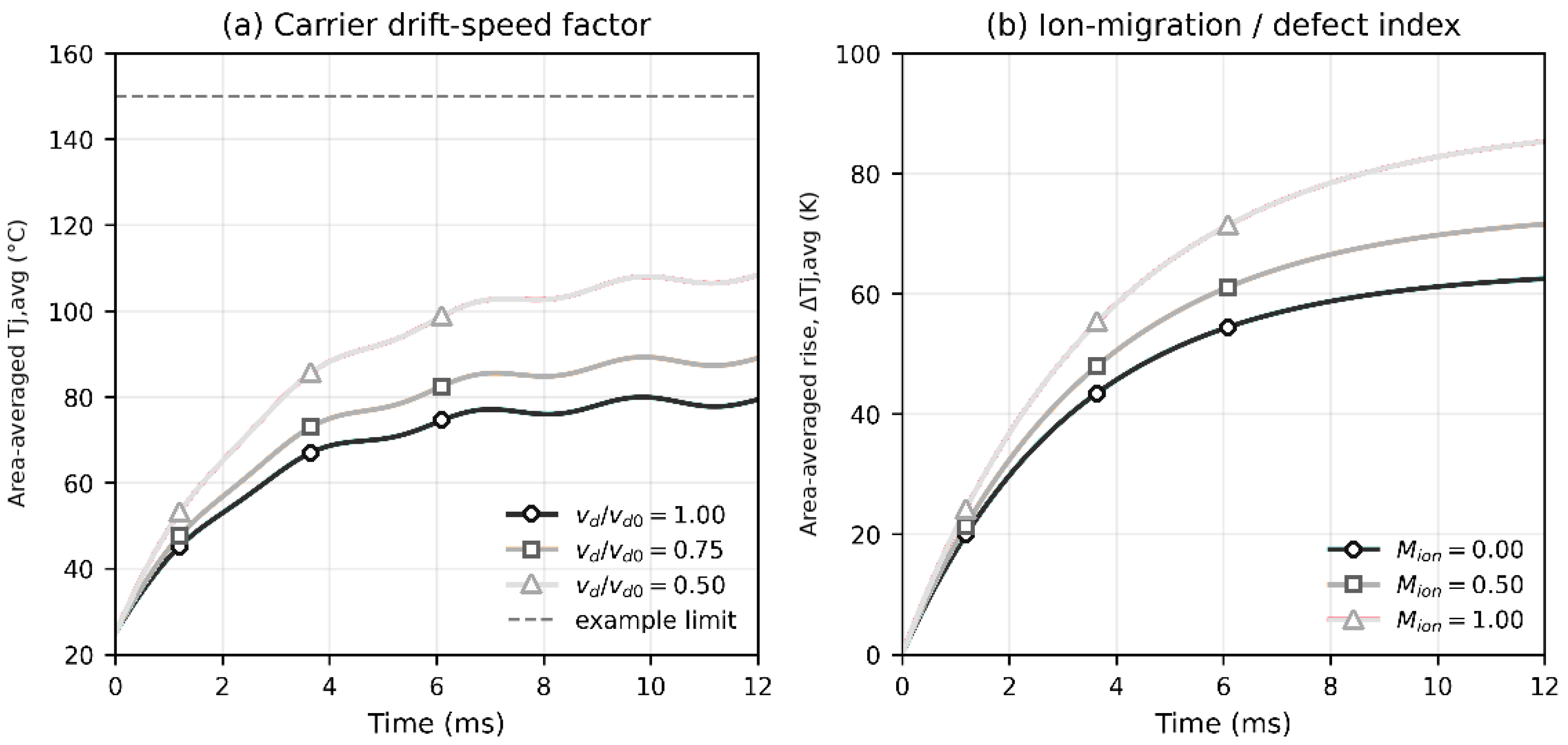
Figure 7 is a normalized sensitivity calculation, not a direct measurement of a device-specific microscopic state. In the left panel, v*d = vd/vd,ref, where vd,ref is the reference drift speed at the baseline material state. The applied-current demand is kept conceptually fixed. Because J = qnvd and, in the low-field limit, vd = μE, a reduction in effective drift speed or mobility requires a larger field, carrier density, or conducting area to maintain the same current; the associated J·E dissipation and on-state voltage therefore increase. The normalized parameter levels are selected to span the reference-calibrated mobility trends in Refs. [14,22,23,24], not to reproduce a measured sample. The plotted Tj,avg curves are lumped, area-averaged first-order thermal responses rather than local hotspot temperatures. Their separation grows with time because the electrical penalty changes the asymptotic heat input, while the small oscillation represents periodic electrical excitation before slower package states have equilibrated.
The right panel introduces Mion as a bounded screening index normalized to [0, 1], where zero denotes the baseline resistance state, and one denotes the upper parameterized perturbation used in the calculation. It is not a measured ion concentration, a damage fraction, or evidence that ions carry the principal device current. Instead, it groups slow processes activated by temperature and electric field, including motion of mobile impurities or charged defects, vacancy redistribution, metal-atom electromigration, interface-trap growth, and loss of effective contact area [15,18,19,20,21]. Increasing Mion is represented by prescribed simultaneous growth of electrical resistance and interfacial thermal resistance. The resulting ΔTj,avg curves therefore quantify model sensitivity to the assumed perturbation only; physical calibration requires impedance, power-cycling, or interface measurements for the same package.
The curves also illustrate the positive feedback that must be retained in junction-temperature prediction. As Tj,avg rises, mobility and thermal conductivity decrease, increasing loss and chip thermal resistance. Higher temperature simultaneously accelerates defect kinetics and migration-like aging processes, which can raise contact resistance further. A model that prescribes constant power and constant material properties will therefore underpredict both the peak and the accumulated mean temperature when this feedback is strong.

4.2. Layered Packaging and the Heat-Spreading Angle

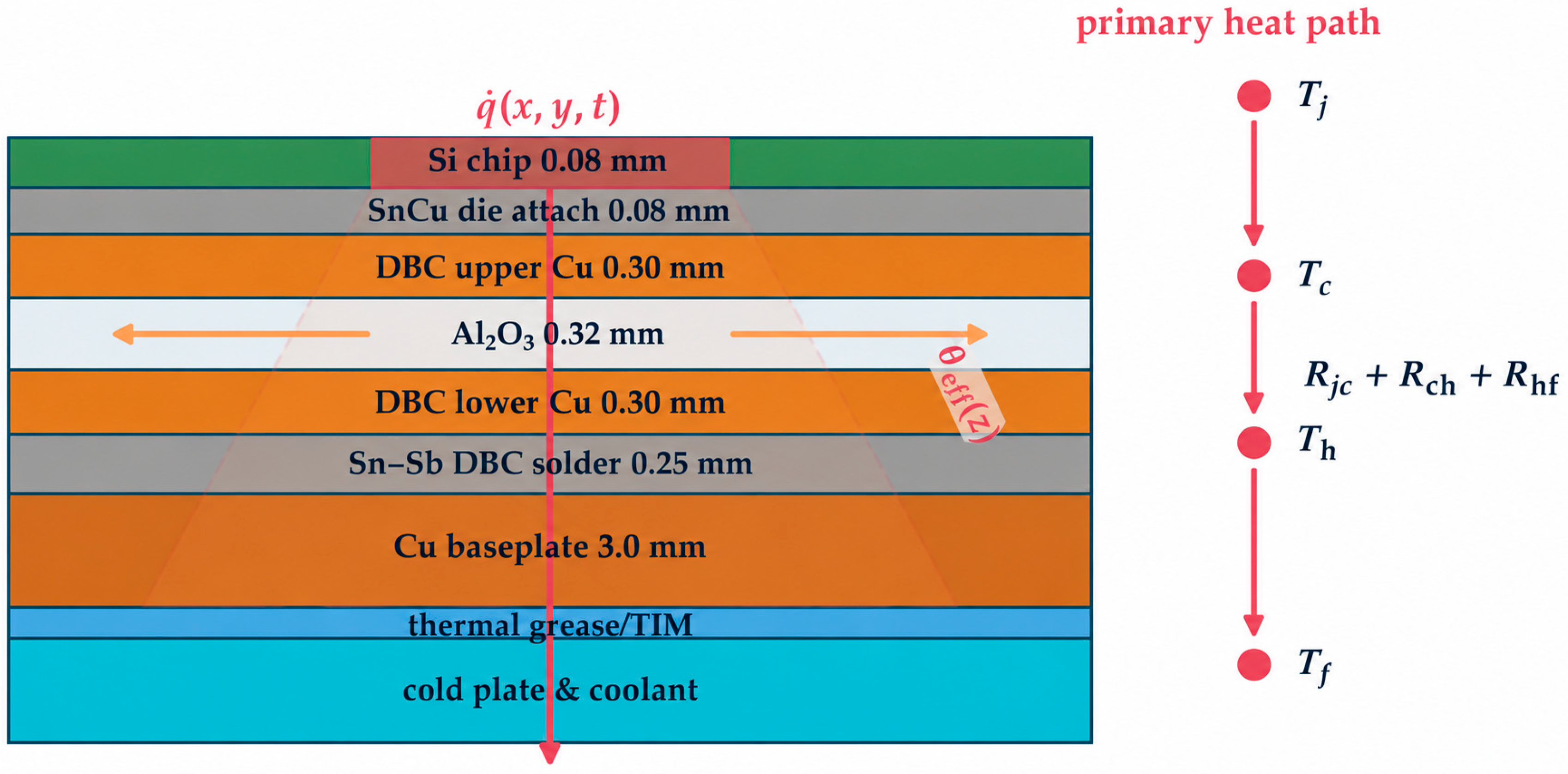
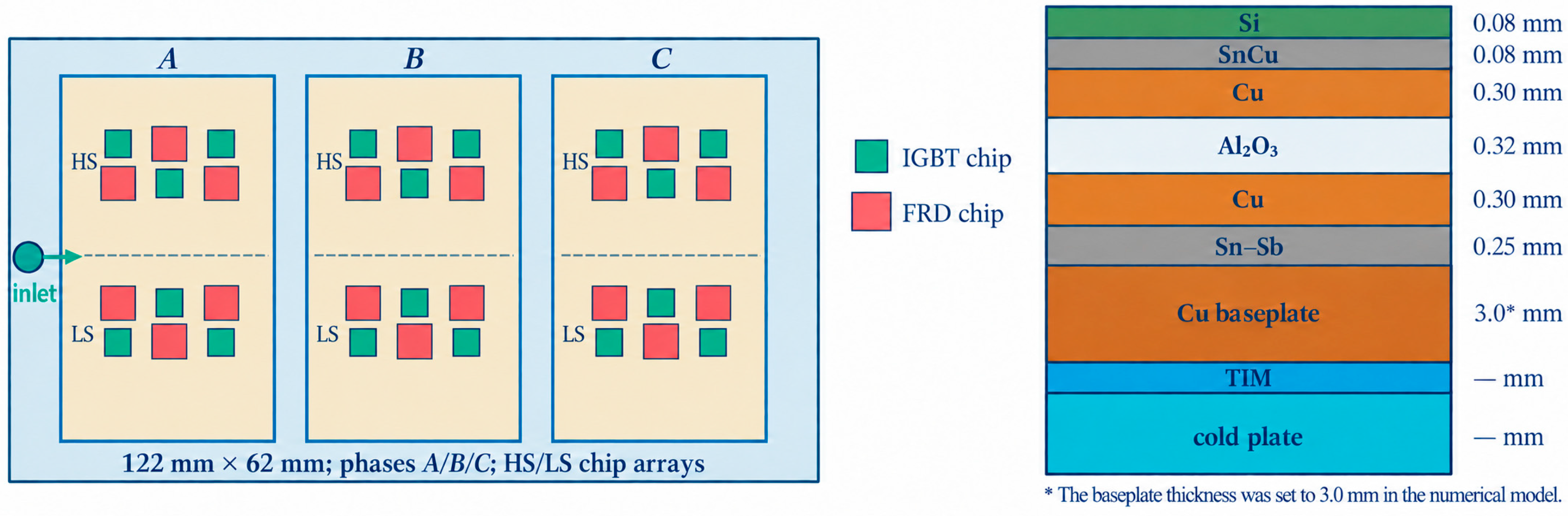
Figure 8 shows the macroscopic heat-transfer path from chip to cold plate. Heat first enters the SnCu die attach and upper DBC copper. Because copper has high kappa, it spreads heat rapidly in the lateral direction. By contrast, the thermal conductivity (κ) of Al2O3 is only approximately 20–24 W/(m∙K), producing marked heat-flow refraction and temperature gradients at its interfaces. The lower copper and baseplate spread the heat again before it crosses the thermal interface material into the cold plate. Solder voids, interfacial roughness, and aging can be represented by a contact resistance R_tc or an equivalent thin layer. In a multichip module, a single vertical path cannot describe mutual heating in the shared copper and baseplate; off-diagonal coupling terms must be retained.
For a rectangular heat source of initial dimensions a × b and a local spreading angle θi in layer i, the effective area at depth z is Ai(z) = [ai + 2z tanθi][bi + 2z tanθi]. If κi is approximately uniform, the thermal resistance and capacitance are given by Equation (16). For ai not equal to bi, integration gives the closed form in Equation (16); for ai = bi, it reduces to Rth,i = Li/[κi × ai(a_i + 2Li tan(θi))]. The thermal capacitance follows directly from integration of the spreading volume and retains terms in L, L2, and L3 [25,26,27].
R t h , i = 0 L   d z / κ i T A i z   ; C t h , i = 0 L   ρ i   c i T A i z d z
R t h , i = l n b i a i + 2 L i t a n θ i / a i b i + 2 L i t a n θ i / 2 κ i   t a n θ i b i a i
C t h , i = ρ i c i a i b i L i + a i + b i t a n θ i   L i 2 + 4 / 3 t a n 2 θ i   L i 3
A fixed angle is valid only when the source is much smaller than the supporting layer, the conductivities of adjacent layers are comparable, and the spreading front has not reached a boundary. This study instead determines θeff from the three-dimensional heat-flux field. On each depth plane, the cumulative normal heat flow is evaluated; the equivalent radius r95(z) enclosing 95% of the total flow is identified; and the layerwise angle is obtained from θeff(z) = arctan{[r95(z) − r0]/z}. This definition automatically captures heat-flow contraction in the ceramic, truncation at module boundaries, and overlap between neighboring chip heat flows.
θ e f f z = a r c t a n r 95 z r 0 / z ; A r 95 q n d A = 0.95 A   q n   d A
Δ T s = Z t h s P s , Z t h , i j 0   i j   f o r   l a t e r a l   c h i p   c o u p l i n g
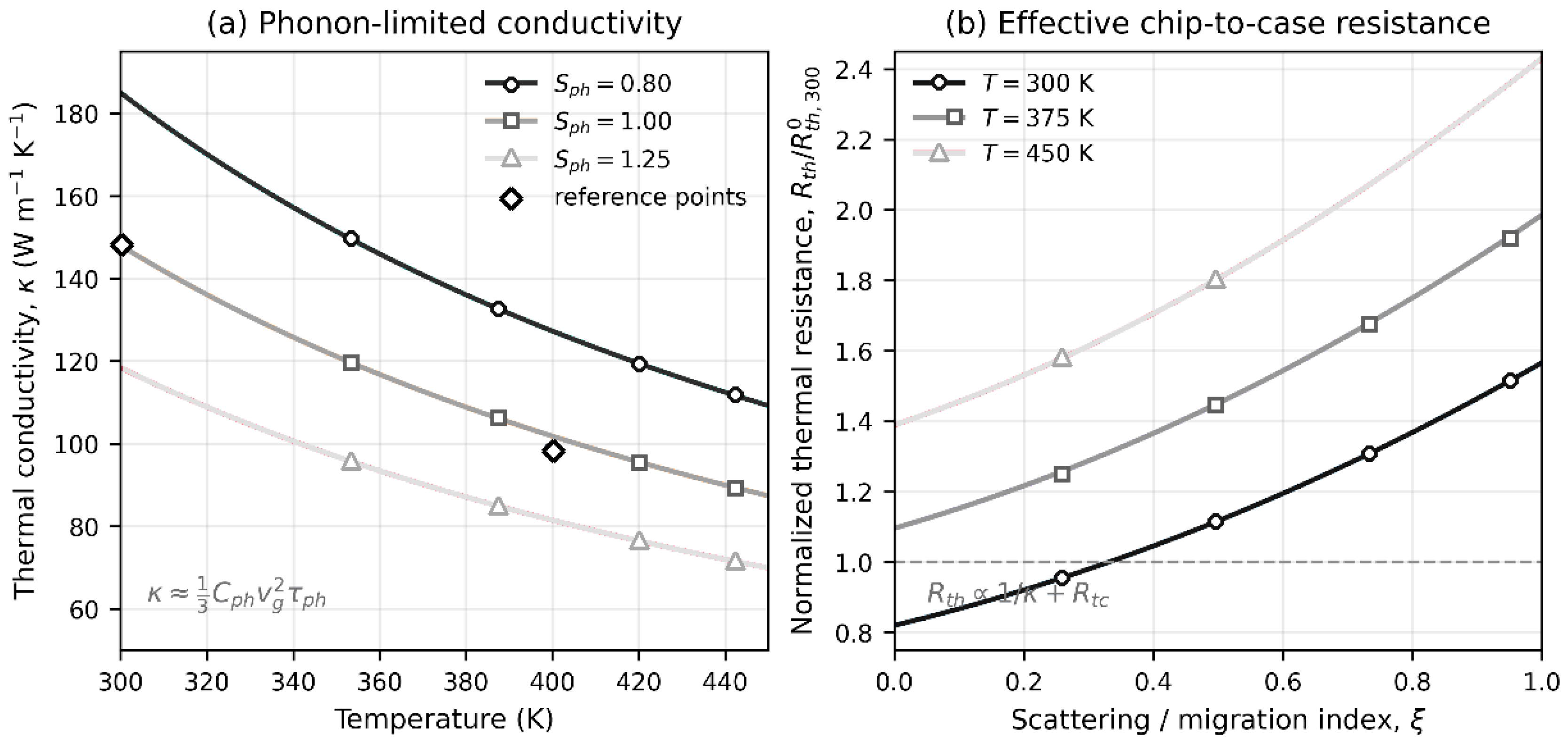
Figure 9 translates the reference-calibrated scattering trends in Refs. [22,23,24] into two quantities used by the package model. Within the relaxation-time approximation, κ ≈ (1/3)Cphvg2τph. Temperature increases phonon population and anharmonic scattering; impurities, vacancies, dislocations, irradiation damage, and boundaries provide additional scattering channels. In the left panel, κ therefore decreases with temperature and with the dimensionless multiplier Sph = τph,refph, where Sph = 1 is the reference scattering state. The markers at 300 and 400 K correspond to the representative silicon values in Table 2. Sph is a compact sensitivity parameter for combined mean-free-path reduction, not a universal material constant or a directly calibrated property of the sample chip.
The right panel reports R*th,jc = Rth,jc/Rth,jc,ref, where the reference value is the undisturbed 300 K model state. For fixed layer thickness and area, the bulk contribution varies approximately as 1/κ; the package resistance also contains interfacial terms Rtc that are sensitive to voiding, delamination, roughness, metallization degradation, and pressure-dependent contact area [27]. The index ξ is normalized to [0, 1] over the prescribed perturbation range and increases both the bulk-scattering and contact-resistance terms. It is not a calibrated damage variable. Even at ξ = 0, the 375 and 450 K curves lie above the 300 K baseline because silicon conductivity is lower. As ξ grows, the curves become nonlinear because the decrease in τph raises bulk resistance while the added Rtc produces an interface drop. The curves therefore indicate relative sensitivity within the stated parameterization rather than device-specific degradation or remaining life.
From a design perspective, the curves show why thermal resistance is a state-dependent property rather than a fixed catalog value. Local hotspots sample a smaller effective area than the whole chip, so their resistance can rise faster than the one-dimensional estimate. At higher temperatures, the same loss produces a larger gradient; that gradient increases thermomechanical strain, promotes defect growth, and can further reduce the effective heat-transfer area.

4.3. Cold Plate and System Boundary Conditions

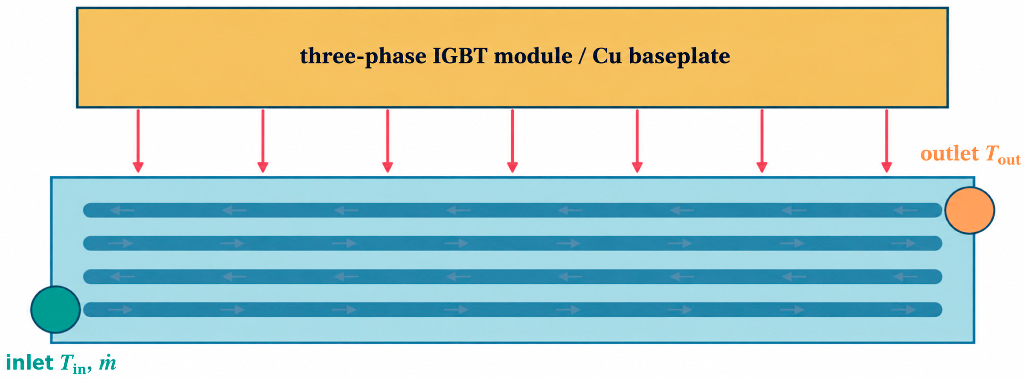
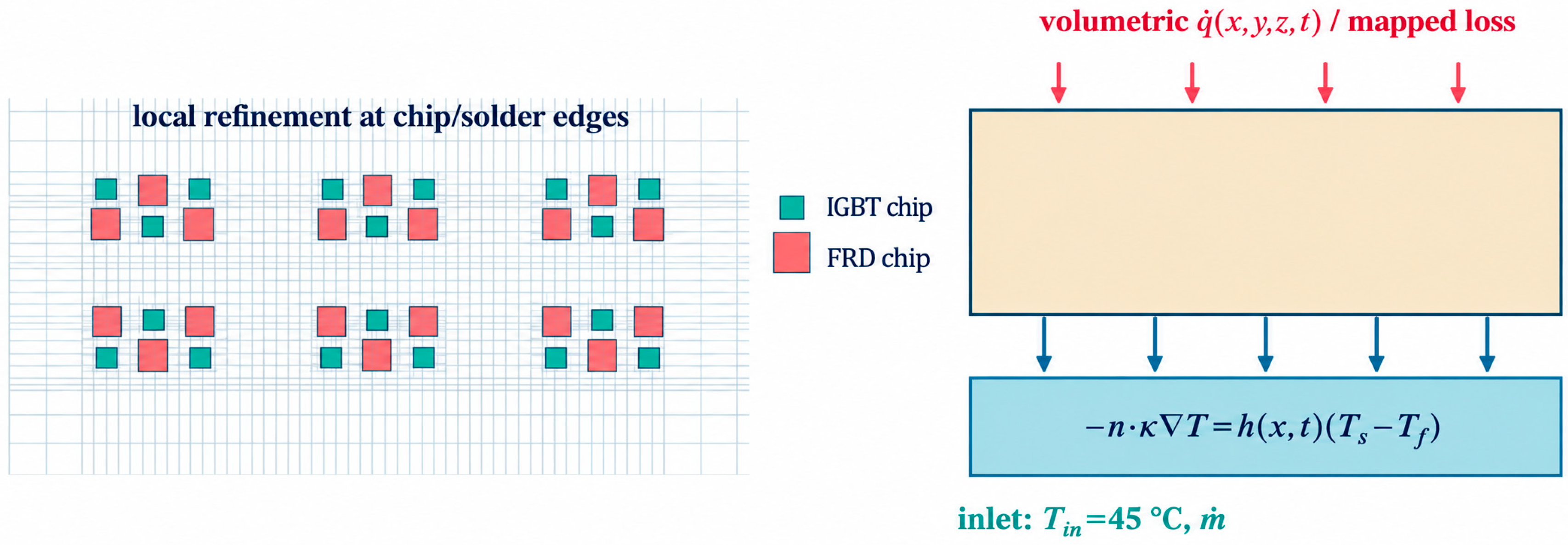
Figure 10 shows the cold-plate flow channels, spatial heat transfer coefficients, and module-coolant energy boundaries. A prescribed-temperature boundary T = Tc implicitly assumes zero cold-plate resistance, no coolant-temperature rise, and an infinite local convective coefficient h; it is therefore appropriate only as an ideal reference. In a real cold plate, the inlet boundary layer is thin, and h is relatively high, while the coolant warms along the flow direction and may be distributed unevenly. Bends, manifolds, and local jets make h strongly nonuniform. Equation (21) should thus be applied as the basic module-bottom boundary; where necessary, Fluent(v.2022 R1) solves continuity, momentum, and energy equations and exchanges wall temperature and heat flux bidirectionally with the solid model. System optimization must constrain not only junction temperature but also pumping power, pressure drop, interphase temperature difference, outlet temperature rise, and cavitation or boiling margin. For single-phase liquid cooling, the flow field may be updated every 0.01–1 s using cycle-averaged loss supplied to the solid. Short-circuit and avalanche events require smaller steps in a local chip submodel, after which released energy and peak temperature are returned to the system model [29,30,31].
n · κ T = h x , y , t T s T f x , y , t
Q · w a l l = m · c p T o u t T i n   ; P p u m p = Δ p V / η p

5. Closed-Loop Cross-Scale Multiphysics Architecture

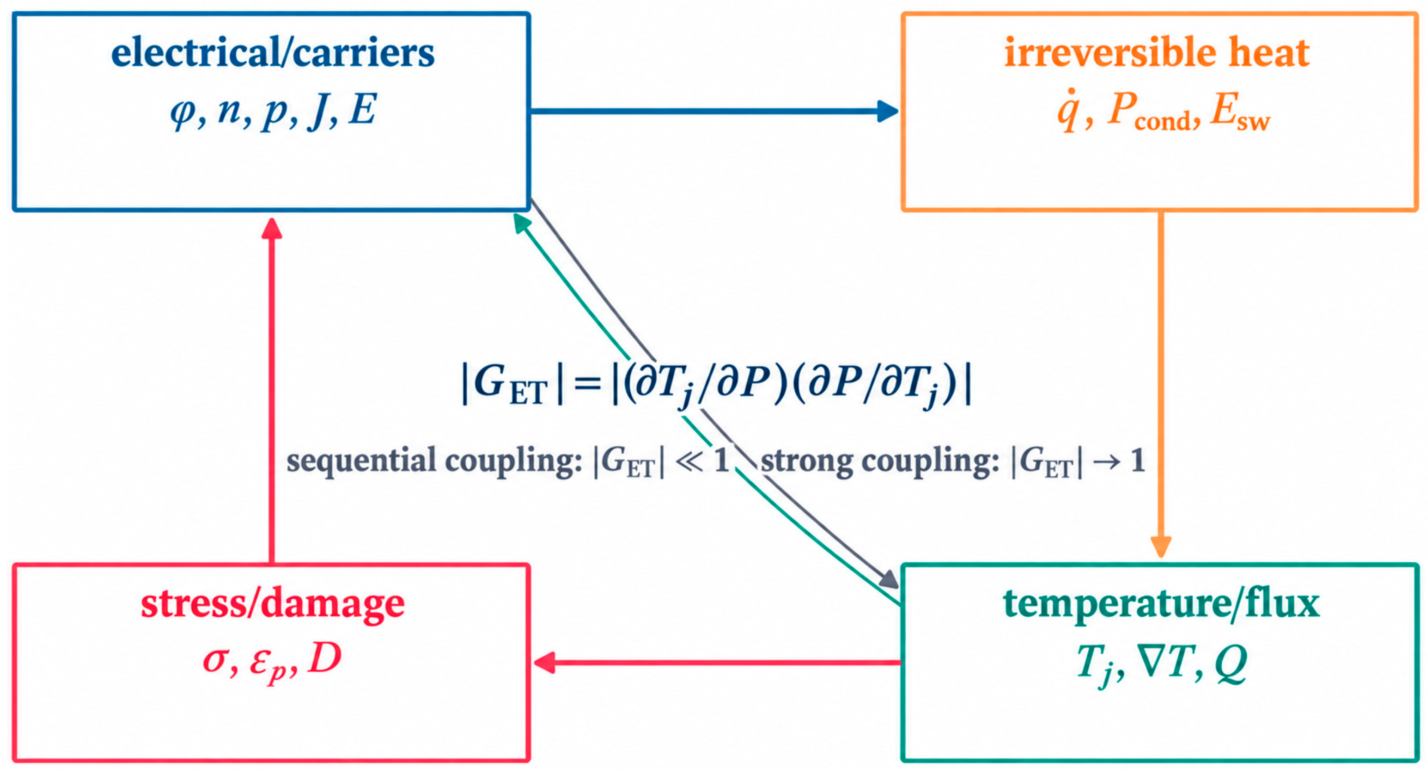
The foregoing analysis yields the closed-loop relationship among the electric field and carriers, heat sources, temperature, and stress or damage shown in Figure 11. The arrows represent both energy transfer and parameter dependence. Electric fields and carriers form irreversible heat sources through J·E dissipation, recombination, and avalanche processes; these sources determine the selected junction-temperature observable and the temperature gradient. Thermal-expansion mismatch converts the temperature field into solder shear, bond-wire plasticity, and interfacial delamination. Damage then increases electrical and thermal contact impedances and redistributes current toward undamaged regions. The central gray path denotes state dependence that cannot be assigned to a single field, including the simultaneous influence of temperature on carrier lifetime, damage on effective area, and coolant flow on the bottom boundary [1,2,15,21].
R e x e , T , D = 0   ; R t T , x e , u , D , h = 0   ; R m u , T , D = 0   ; R f h , T f , T s = 0
G E T = T j / P l o s s P l o s s / T j
σ = C : ε α C T E T T r e f ε p ε c r
When |GET| is much less than unity and parameters change slowly within one macro step, a single sequential transfer is sufficiently accurate. When |GET| approaches unity, damage induces current crowding, or the cooling boundary changes abruptly, the electrical, thermal, mechanical, and fluid subproblems must be iterated within the same macro step. Local stability requires |GET| < 1, but this does not make the error from neglecting feedback acceptable; a large ∂P/∂T can still produce a substantial peak-temperature bias. Strong coupling employs Aitken relaxation or Newton updates while simultaneously monitoring temperature residual, power residual, and interfacial energy imbalance.
The time steps in Table 4 are exchange intervals rather than all internal discretization steps. This distinction avoids two common errors: solving the complete cold plate with a nanosecond device step, which is unnecessarily expensive, and feeding a seconds-scale mean temperature back into a microsecond switching transient, which suppresses peak feedback. In the multirate method, electrical loss is integrated over a switching period before being transferred to the thermal field, whereas fault pulses are resolved explicitly in a local chip submodel. The cold plate updates h and Tf on a slower macro step, and damage is updated at thermal-cycle extrema or by cycle jumping. The device model may use finer steps within a switching period, but the quantity sent to the thermal model is the energy-conserving period integral. Mechanical analysis may be performed only at cycle maxima and minima with cycle jumping. The control model receives reduced Tj,max, Tj,avg, and life-consumption states rather than the full three-dimensional field. This hierarchical synchronization balances computational cost and mechanism fidelity.

6. Numerical Implementation and Model Verification

The terms verification, validation, and comparison are used here in their standard modeling senses. Verification establishes that equations are solved and coupled correctly through mesh and time-step convergence, conservation residuals, and implementation checks. Validation requires comparison with independent measurements for the same observable, geometry, loading, and boundary conditions. Comparison denotes a descriptive assessment among analytical, equivalent-field, finite-element, and reduced-order outputs after observable and boundary definitions are aligned. This study is primarily a theoretical and computational investigation. Because no matched thermography, TSEP, thermocouple, or bench-test data are reported for the parameterized module, the quantitative evidence supports numerical verification and cross-model consistency only; it does not establish experimental predictive accuracy.

6.1. Model Construction and Mesh Independence

Using the sample package parameters in Table 3 and the geometry and cooling practices summarized in Refs. [25,26,27,28,29,30,31], the model employs a 122 mm × 62 mm copper baseplate with phase modules A, B, and C arranged along its length. Each phase is divided into high-side and low-side bridge arms and contains three IGBT-FRD groups. Figure 12 and the local mesh in Figure 13 are computational constructions for this parameterized sample; the NTC location, inlet, and chip numbering define the monitoring regions and cold-plate flow direction.
The mesh is refined through the chip thickness, solder layers, DBC edges, termination, bond-wire feet, and high heat-source-gradient regions, and is progressively coarsened in the copper baseplate and far-field cold plate. Each thin layer contains at least three quadratic elements or five linear elements to resolve the interlayer temperature drop. The time step must resolve both the source pulse and the smallest thermal time constant. An energy-equivalent load permits larger steps for cycle-averaged operation, but short-circuit and avalanche events must be resolved directly. Mesh and time-step acceptance are based jointly on Tj,max, total heat flow, and interlayer temperature drop rather than mean temperature alone.
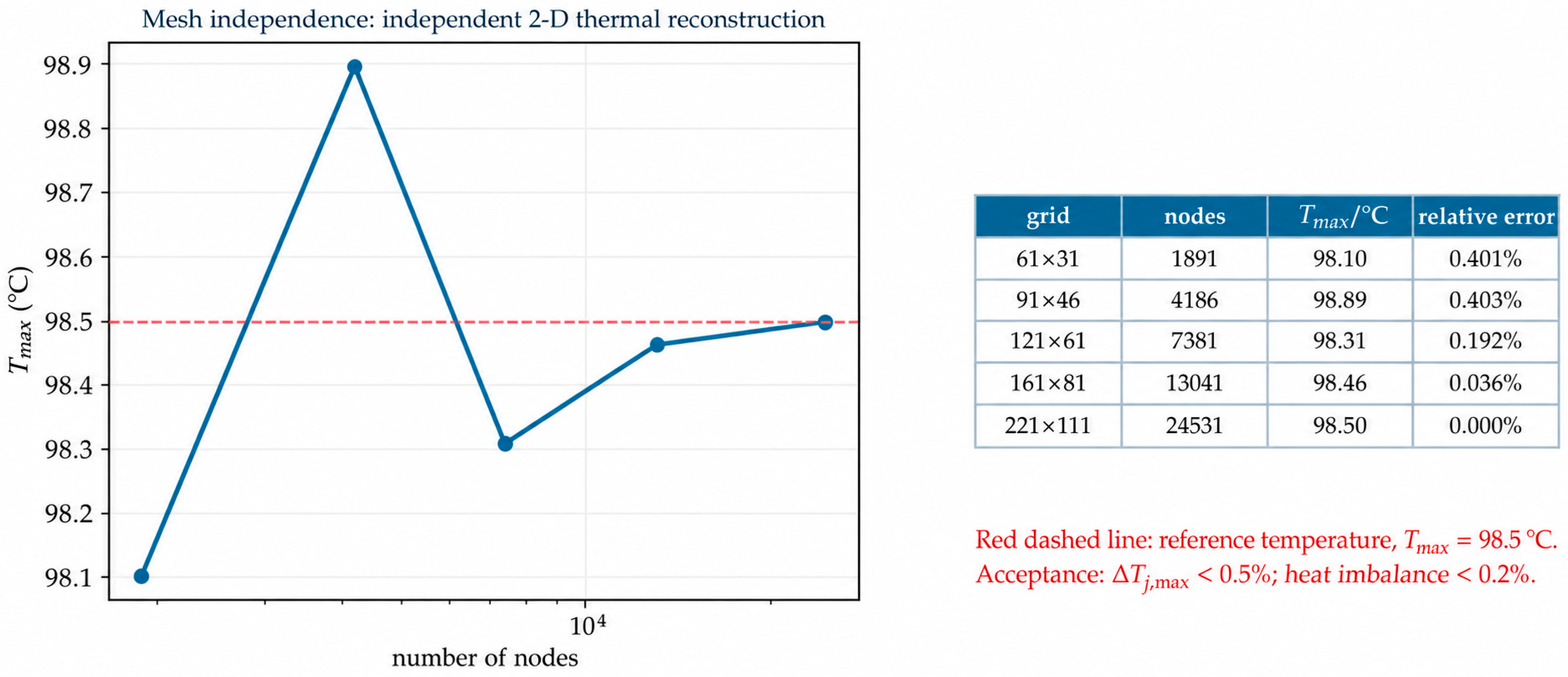
Figure 14 uses an independently discretized two-dimensional diffusion equation consistent with the three-phase geometry and is not raw output from a commercial solver. Because rectangular source boundaries align differently with successive grids, the coarse-grid results are mildly nonmonotonic. Refinement from 161 × 81 to 221 × 111 changes Tmax by approximately 0.04%, satisfying the 0.5% criterion.

6.2. Coupling Implementation and Convergence Criteria

Figure 15 distinguishes the computations implemented in this study from interfaces retained for future end-to-end coupling. The implemented subset comprises reference-calibrated property tables, terminal conduction/switching/reverse-recovery loss calculation, energy-normalized spatial heat-source assignment, analytical and two-dimensional diffusion reconstruction, three-dimensional finite-element thermal calculation, and Cauer reduction. The cold-side calculations prescribe h(x,t) and coolant-temperature rise from the parameter ranges in Refs. [29,30,31]; a new two-way Fluent conjugate-heat-transfer solution is not claimed. Likewise, the reported thermomechanical outputs are a constrained equivalent-stress proxy and the dimensionless D* screening index, not a calibrated ANSYS (v.2022 R1) Mechanical (v.2022 R1) fatigue, creep, delamination, or lifetime solution. Full device-specific DFT/DFPT, TCAD source export, bidirectional CFD exchange, and calibrated mechanical damage updating are shown as compatible framework extensions rather than as completed links in the quantitative chain.
Sequential coupling is appropriate when |GET| is small, the cooling boundary varies slowly, and operation is normal. Strong coupling is required for short circuits, overload, pronounced temperature coefficients, boiling, or damage-induced contact discontinuities. Within each macro step, P(k+1) = P(Tk, Dk), T(k + 1) = T(P(k+1), hk), and h(k+1) = h(Ts(k+1)) are updated successively until |ΔTj| < 0.1 K and |ΔP|/P < 10−3.

7. Results and Discussion

All quantitative results in this section are generated by the parameterized analytical, equivalent-field, finite-element thermal, or reduced-order models using the sample inputs in Table 2 and Table 3 and the cited reference-calibrated ranges. Convergence and conservation studies verify numerical implementation, whereas agreement among representations is reported as cross-model comparison. The literature measurements and property studies provide input ranges and physical context, but they do not constitute experimental validation of the present geometry, loading, cooling boundary, or temperature observable.

7.1. Equivalent-Field Reconstruction and Cross-Scale Interpretation

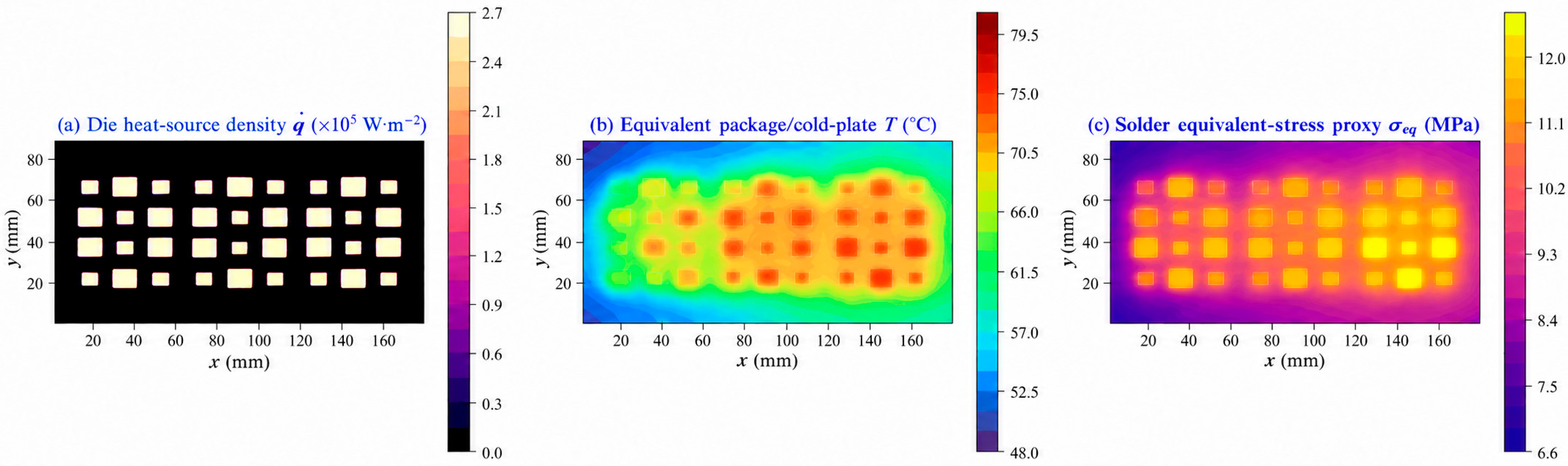
Using the sample layout and source parameters in Table 3 together with the package and cooling relations in Refs. [25,26,27,28,29,30,31], an equivalent case is calculated with 36 staggered IGBT/FRD heat sources across three phases, a 45 °C inlet, a 5 K coolant rise, and h decreasing from 3100 to 2000 W m−2 K−1. The modeled temperature ranges from 49.1 to 79.6 °C, and the domain-area-averaged package temperature is 64.2 °C. The inlet-to-outlet difference arises from the combined variations in Tf and h, whereas local peaks within a phase are governed by IGBT/FRD loss, chip spacing, and superposed spreading in the copper layers. The constrained-stress proxy reaches approximately 12.6 MPa near large gradients and chip edges. These values are parameterized computational outputs, not measured module data or calibrated reliability quantities.
Figure 16 shows the calculated spatial coupling among energy-normalized heat-source weights, the equivalent package/cold-plate temperature field, and a solder-layer constrained-stress proxy, using the sample parameters and physical relations in Refs. [17,18,19,20,21,25,26,27,28,29,30,31]. In Figure 16a, multiple rectangular sources are arranged in an array, and their heat fluxes span 0–2.7 × 10⁵ W/m2. Larger chips or higher assigned loss form stronger local sources, making module heat input discrete and spatially nonuniform. The differences are prescribed through normalized rectangular weights representing chip type, conduction current, switching loss, and unequal current sharing. At every coupling step, the weights are divided by their volume integral so that the integrated q · equals the calculated terminal device loss.
Figure 16b presents the equivalent package/cold-plate temperature field, which ranges from approximately 48 to 79.5 °C. Lateral conduction and cold-plate convection spread and superimpose the discrete sources, producing a continuous field that extends beyond individual chip boundaries. Local temperature peaks remain visible at chip locations, confirming strong spatial correspondence between the source array and hotspots. Along the x direction, temperature first increases and then decreases slightly, with the hottest region located near the center-right of the module. This pattern reflects superposition of several high-flux chips, differences in edge cooling, and coolant heating along the flow path. Lower temperatures near the perimeter result from the combined effects of boundary cooling and lateral diffusion.
Figure 16c shows the constrained solder-stress proxy, ranging from approximately 6.6 to 12 MPa. High values are concentrated in the center-right region and broadly coincide with the high-temperature zone in Figure 16b. The proxy uses an effective linear thermoelastic constraint relation with material ranges informed by Refs. [17,18,19,20,21]; it is not a solved elastoplastic fatigue or creep field. Its spatial pattern indicates where thermal-expansion mismatch and large temperature gradients may elevate mechanical demand. Accordingly, the result supports qualitative risk localization only and does not establish solder life, crack-growth rate, or delamination probability.
From a scale-mechanism perspective, the source nonuniformity in Figure 16a originates from carrier-current paths and switching states. Package diffusion smooths the field in Figure 16b while preserving identifiable local hotspots. Figure 16c is more sensitive to temperature gradient and thermal-expansion mismatch, making solder ends and chip edges critical regions. At material scale, decreasing κ(T) reduces thermal diffusivity; at carrier scale, μ(T) and τ(T) modify J·E and tail-current duration; at chip scale, the diffusion length in Equation (15) determines the activated thermal mass; at package scale, copper spreading and ceramic resistance set interlayer drops; and at system scale, h and Tf define the mean-temperature baseline. Figure 6 and Figure 16 thus show that upscaled parameters are continuously updated functions of temperature rather than one-way constants.

7.2. Multichip Thermal Coupling and Interphase Propagation

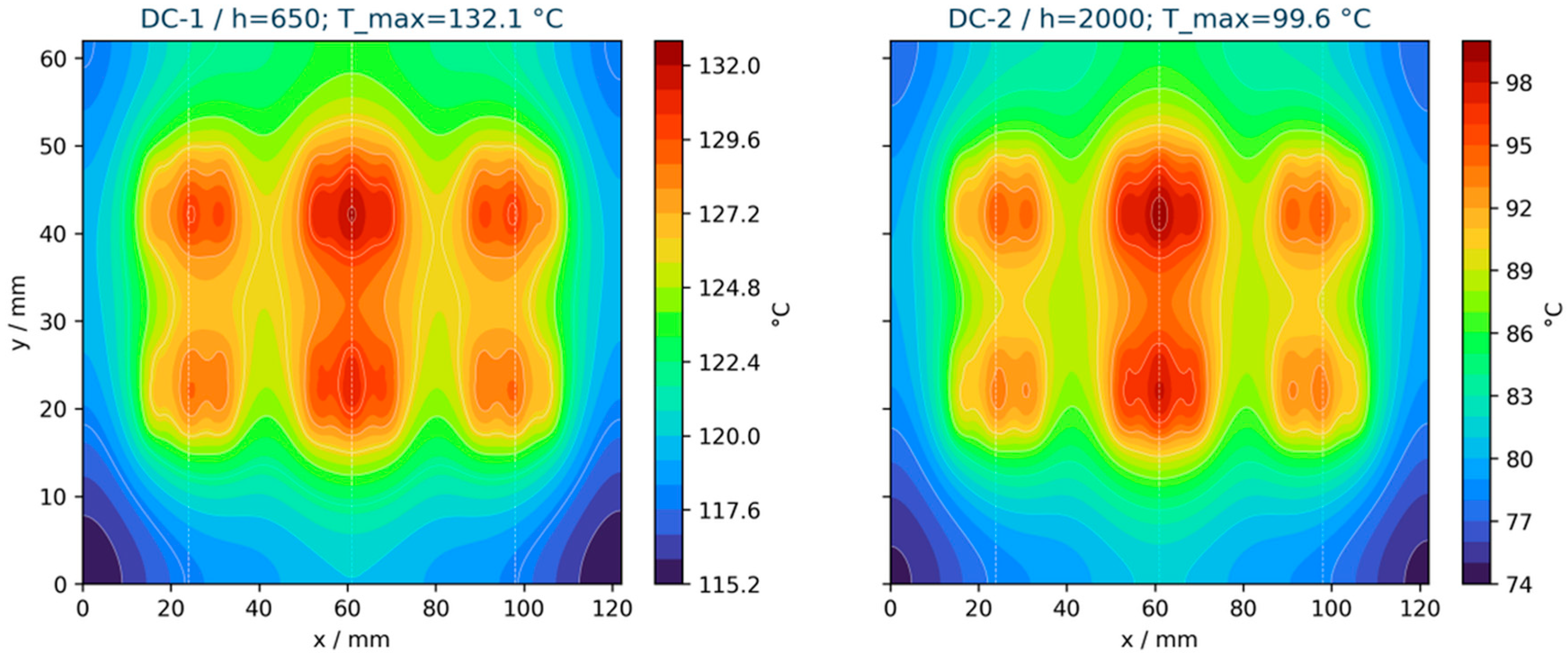
Figure 17 compares two independent two-dimensional reconstructions under prescribed cooling boundaries to examine hotspot location, interphase coupling, and convection sensitivity. The sample heat-source layout and material ranges are taken from Table 2 and Table 3 and the modeling relations in Refs. [25,26,29,30,31]. The left and right panels correspond to DC-1 and DC-2, with h = 650 and 2000 W m−2 K−1, respectively; their modeled maxima are 132.1 and 99.6 °C. This is an illustrative parameter sensitivity calculation and not a measured cooling-performance comparison.
Six principal source regions are present, and a local peak forms above each chip, showing that device loss is first concentrated in the active regions and then spreads through the package. Overlap between neighboring diffusion regions creates a continuous high-temperature band near the module center. The central chip column is hottest because it receives both self-heating and heat coupled from the left and right. Side chips are cooler because proximity to the module boundary provides more lateral spreading space. The lowest temperatures occur around the perimeter, especially at the two lower corners, reflecting the combined effects of boundary cooling and two-dimensional diffusion.
Under DC-1, the lower prescribed heat-transfer coefficient limits rejection at the model boundary, producing a higher temperature field and connected hotspot regions. Increasing h to 2000 W m−2 K−1 in DC-2 lowers the modeled maximum by approximately 32.5 °C, contracts the isotherms toward the sources, and enlarges the peripheral low-temperature region. Within this parameterized reconstruction, stronger convection reduces the overall temperature rise and hotspot extent. The central column nevertheless remains hottest, indicating that changing h alone does not remove nonuniformity arising from source layout and interphase thermal coupling. The numerical reduction is not an experimentally validated performance claim for a specific cold plate.
Overall, the module temperature field is governed jointly by chip-loss distribution, lateral package diffusion, neighboring-source coupling, and the cooling boundary. A higher heat-transfer coefficient markedly reduces maximum temperature, but further uniformity requires coordinated optimization of chip spacing, power balance, and cold-plate channel layout to weaken central heat accumulation.

7.3. Finite-Element and Cauer Models

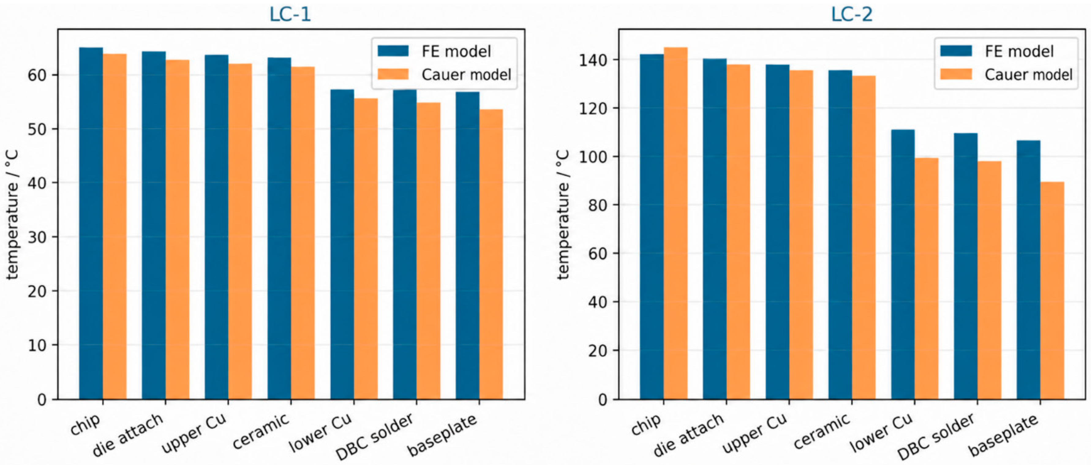
Figure 18 compares layer-representative temperatures from finite-element and theoretical Cauer models under cases LC-1 and LC-2, using the material stack in Table 3 and the compact-model relations in Refs. [10,11,12,25,26,27]. From left to right, the horizontal axis represents the chip, die attach, upper DBC copper, ceramic, lower DBC copper, DBC solder, and baseplate. Both methods produce a progressive decrease from chip to baseplate, consistent with the imposed heat-flow path. The reported metrics quantify cross-model differences and do not represent error against experimental truth.
Under LC-1, the layer-representative chip temperature is approximately 64–65 °C, and the two models differ little near the chip. Their difference increases toward the cold side: the finite-element model gives a baseplate temperature near 59 °C, whereas the Cauer model gives about 54 °C. Under LC-2, the layer-representative chip temperature is about 142–145 °C. The difference remains within several degrees through the chip, die attach, upper copper, and ceramic, but grows from the lower DBC copper onward. The finite-element lower copper, DBC-solder, and baseplate temperatures are approximately 111, 110, and 106 °C, compared with about 99, 97, and 89 °C from the Cauer model. These are model-specific layer outputs rather than Tj,max or a sensor reading. The larger cold-side difference is attributable to the boundary mismatch and shows the limitation of comparing a prescribed-temperature Cauer termination with a finite-h finite-element boundary.
Table 5 gives seven-layer mean absolute and root-mean-square cross-model differences of 3.61 and 4.12 K under LC-1 and 6.92 and 9.27 K under LC-2. The mean relative difference across the four chip-side layers is 1.28–2.98%, whereas that across the three cold-side layers is 9.54–12.56%. These percentages are descriptive normalized differences between aligned model outputs, not prediction errors against measured truth. The pattern arises primarily from different terminal boundary types: the Cauer chain ends at a prescribed-temperature node, while the finite-element model applies finite h at the bottom surface. Increasing the final-layer resistance to fit one case would obscure rather than resolve that boundary inconsistency.
The result also explains the distinction between maximum- and mean-junction-temperature models. A local network derived from geometry and spreading angles preserves the area expansion near the source and more closely represents the infrared-observable maximum temperature, Tj,max. A structure–function extracted from a TSEP cooling curve inherits current weighting and is therefore closer to Tj,J. Neither approach is inherently correct or incorrect; each represents a different observation operator, and their outputs should be compared only after the spatial weighting and temporal bandwidth have been aligned.

7.4. Dynamic Temperature-Loss Feedback

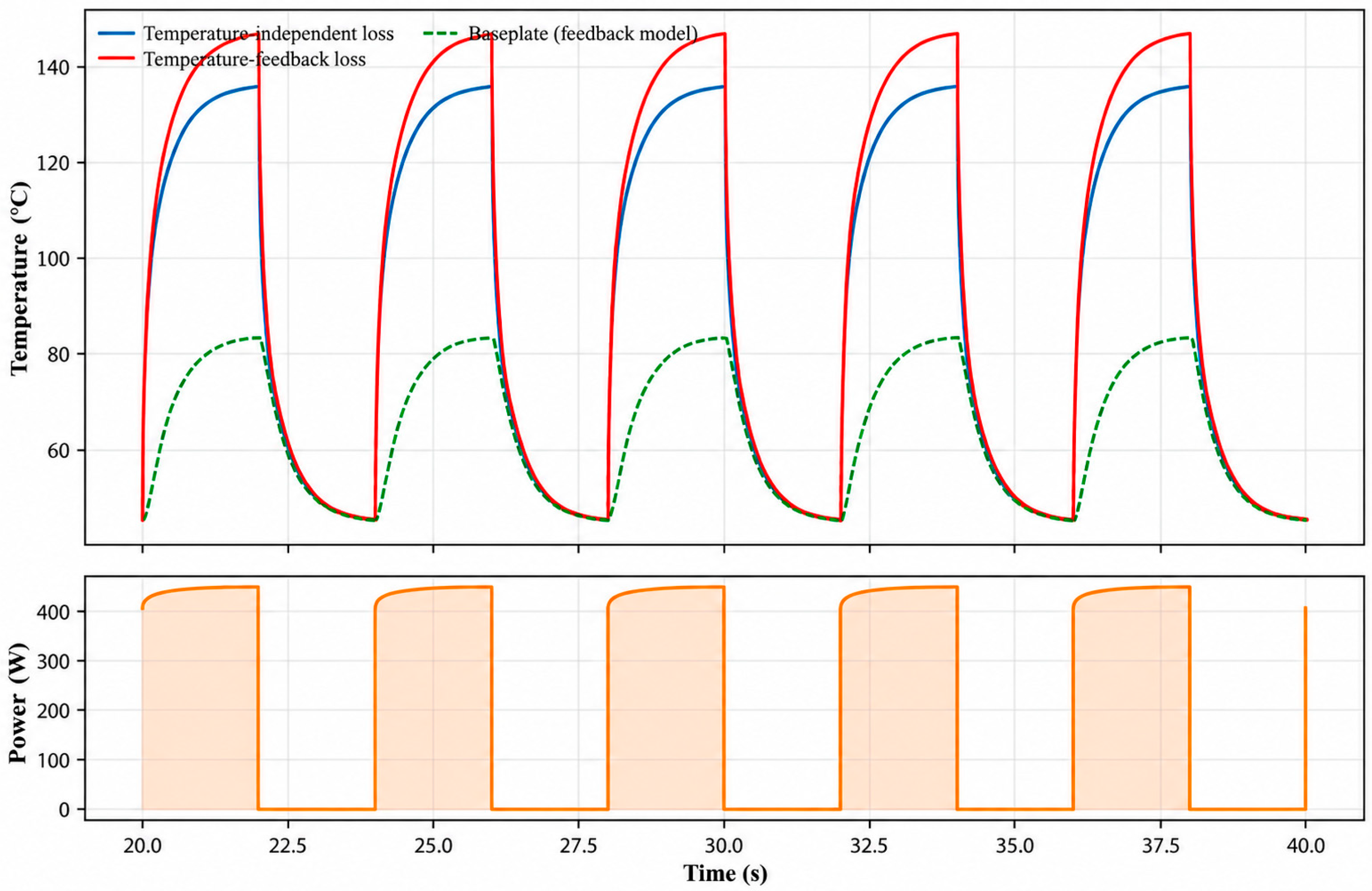
Figure 19 shows the response of a lumped Cauer chip-temperature state, interpreted here as Tj,avg, under periodic power loading and compares temperature-independent loss with a temperature-feedback model. The lower panel switches power periodically between zero and approximately 450 W, with each cycle comprising a high-power interval and a zero-power dwell. During the high-power interval, loss rises gradually from about 410 to 450 W as Tj,avg increases; after turn-off, it rapidly falls to zero. The upper panel shows the lumped chip and baseplate temperatures. When power is applied, the chip state rises rapidly, and its growth rate gradually decreases, producing an exponential-like trajectory. After power removal, it falls rapidly and then approaches its lower level more slowly, reflecting the combined thermal resistance and capacitance of the package.
The temperature-feedback calculation produces a maximum lumped chip temperature Tj,avg of approximately 147 °C, compared with about 136 °C from the temperature-independent calculation, a cross-model difference of roughly 11 °C. Conduction voltage, switching energy, and effective resistance are temperature-dependent. Rising junction temperature increases the prescribed device loss, and the added loss raises temperature further. Within this representative Cauer case, omitting feedback therefore gives a lower peak; the magnitude still requires device-specific loss calibration and matched experimental validation before use as a protection threshold.
The baseplate state peaks near 83 °C and changes more gradually because the multilayer package impedes heat transfer while the larger baseplate capacitance attenuates fluctuation. Similar maxima and minima in successive cycles indicate convergence of the model to a stable periodic response. The calculation demonstrates why temperature-dependent loss should be retained when studying area-averaged junction-temperature sensitivity under periodic high-power operation; it does not by itself validate a lifetime model or an overtemperature-protection setting.

7.5. Thermomechanical Fields and Reliability Implications

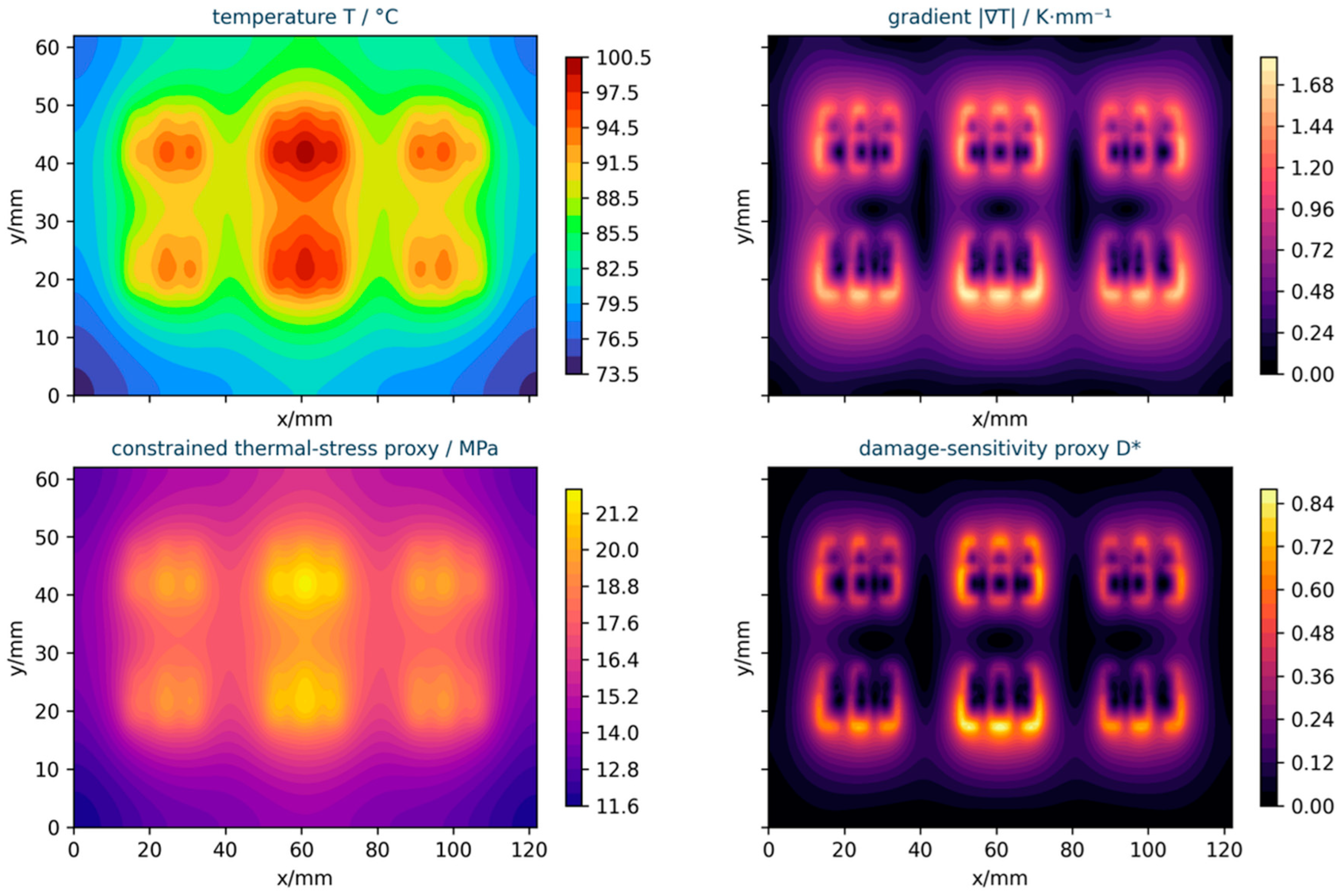
Figure 20 presents a qualitative thermomechanical-risk screening constructed from the parameterized temperature field and material trends in Refs. [17,18,19,20,21]. The upper panels show temperature and |∇T|. The constrained-stress proxy uses the linear relation in Equation (25) with effective elastic and thermal-expansion parameters; it is not a calibrated elastoplastic, creep, or fatigue solution. For the damage-sensitivity proxy, the calculated stress and gradient fields are separately min–max normalized over the plotted domain as σ ^ = (σ − σmin)/(σmax − σmin) and g ^ = (|T| − gmin)/(gmax − gmin), and D* = σ ^ g ^ . Thus, D* = 0 and D* = 1 denote the lower and coincident upper limits of the two normalized fields in this case; they do not represent zero and complete physical damage.
The upper-left temperature field ranges from approximately 73.5 to 100.5 °C. Each chip forms a local high-temperature region, with the central column, particularly its upper chip, approaching 100 °C. Central chips receive both self-heating and laterally coupled heat, whereas side chips have shorter paths toward the module boundary. Temperature decreases continuously toward the package edge and cooling boundary. The upper-right magnitude of the temperature gradient |∇T| reaches about 1.68 K/mm. Unlike the broad hot regions, high gradients form bands and rings at chip edges and local material interfaces. The location of maximum temperature therefore does not necessarily coincide with the maximum gradient; abrupt changes in material, heat flux, and geometry at chip edges produce rapid temperature variation over short distances.
The lower-left constrained thermal-stress field ranges from approximately 11.6 to 21.2 MPa. It is smoother than the gradient field but corresponds broadly to the high-temperature region. Stress is greatest around the central chips because coefficient-of-thermal-expansion mismatch and structural constraint convert nonuniform heating into thermal stress, and overlapping fields from adjacent sources intensify deformation incompatibility. The lower-right damage-sensitivity index D* reaches approximately 0.84 and is concentrated at chip edges, especially around the lower central chip. This index combines temperature gradient and constrained stress, showing that potential damage is governed not by maximum temperature alone but by coincident high stress and high gradient. Central chips and all chip edges are therefore critical reliability regions. Optimizing layout, balancing loss, improving interfaces, and strengthening local cooling can reduce gradients and stress concentrations and suppress solder fatigue, delamination, and crack growth. Consequently, only the case-specific qualitative observation that central-chip and edge regions are potential risk locations is retained; quantitative reliability prediction requires material calibration, uncertainty or sensitivity analysis, and matched power-cycling experiments.

8. Conclusions

This study established an energy-consistent computational framework connecting first-principles-informed material descriptors and carrier mechanisms to prescribed energy-normalized heat sources, chip diffusion, package spreading, multichip coupling, nonuniform cold-side boundaries, qualitative thermomechanical-risk screening, and reduced-order junction-temperature estimation. The principal novelty is the explicit definition of cross-scale energy interfaces, multirate synchronization, and temperature observation operators, rather than the individual thermal-network, finite-element, or multiphysics components. This architecture provides additional discrimination among local hotspots, lumped chip states, sensor-filtered temperatures, and differences caused by incompatible terminal boundaries. The principal findings are as follows.
(1)
For an 80 μm silicon chip at 400 K, the Fourier time τd = L2 is 0.12 ms, while the characteristic penetration length δT = 2√(αt) reaches the chip thickness at 0.030 ms. These criteria are mathematically consistent and describe order-one Fourier equilibration and penetration of the selected diffusion envelope, respectively. Lateral diffusion remains much slower, so the early Tj,max depends strongly on the prescribed spatial source and cannot be inferred from Tj,avg or TNTC.
(2)
At package scale, a heat-flux-defined effective spreading angle represents finite boundaries and overlap between neighboring chip heat flows. In the layerwise finite-element/Cauer comparison, the mean relative cross-model difference is 1.28–2.98% across the four chip-side layers and 9.54–12.56% across the three cold-side layers when the two models use different terminal boundary types. These values quantify consistency between computations, not accuracy against measured temperatures.
(3)
In the illustrative three-phase boundary-sensitivity calculation, increasing h from 650 to 2000 W m−2 K−1 lowers the modeled maximum from 132.1 to 99.6 °C. The result demonstrates the direction and magnitude of sensitivity for the specified parameter set; it is not a measured cold-plate performance claim. The central maximum persists because of the source layout and lateral multichip coupling.
(4)
Electrothermal feedback is quantitatively important: in the representative periodic case, incorporating temperature-dependent loss raises the predicted peak junction temperature by approximately 11 K. Sequential coupling remains efficient when the loop gain is small, whereas rapid boundary changes, high-field events, or damage-induced current redistribution require inner iteration and explicit energy-residual checks. The thermomechanical stress and D* fields, however, are qualitative proxies only and must not be interpreted as calibrated fatigue, creep, delamination, or lifetime predictions.
Accordingly, reliable thermal design should match model resolution to the dominant time and length scales, retain spatially varying coolant conditions for system prediction, and distinguish maximum, area-averaged, current-weighted, and sensor-proximal temperatures. The numerical values reported here define verified mechanistic trends for the parameterized configuration. The numerical results therefore support theoretical interpretation, implementation verification, and cross-model comparison for the parameterized configuration. They do not establish device-specific predictive accuracy or quantitative reliability. Future work will validate the key temperature observables under the same module geometry, electrical loading, and cooling boundary using synchronized infrared thermography, TSEP measurement, and embedded thermocouples; power-cycling and interface characterization will then be used to calibrate the stress/damage relations and test robustness to material, boundary, and geometric uncertainty.

Author Contributions

Conceptualization, Z.Z.; methodology, Z.L.; software, Z.L.; verification, Z.L.; formal analysis, Z.L.; writing—original draft, Z.L.; writing—review and editing, Z.Z. and Z.L. All authors have read and agreed to the published version of the manuscript.

Funding

This research was funded by Chongqing Academy of Science and Technology grant number CSTB2024NSCQ-LZX0158.

Institutional Review Board Statement

Not applicable.

Informed Consent Statement

Not applicable.

Data Availability Statement

The original contributions presented in this study are included in the article. Further inquiries can be directed to the corresponding author.

Acknowledgments

The authors gratefully acknowledge the research and technical support provided by all members of the research team, as well as the financial support provided by the research project associated with this study.

Conflicts of Interest

The authors declare no conflicts of interest.

Nomenclature

SymbolDefinitionUnit
AHeat-transfer or cross-sectional aream2
AeffEffective electrically or thermally conducting aream2
CphPhonon heat capacityJ m−3 K−1
cpSpecific heat capacityJ kg−1 K−1
DDamage-state variable
D*Normalized thermomechanical-risk screening index
DaAmbipolar carrier-diffusion coefficientm2 s−1
EElectric-field magnitudeV m−1
EgSemiconductor bandgapeV
Eon, Eoff, ErrTurn-on, turn-off, and reverse-recovery energyJ
FoFourier number
GETElectrothermal coupling gain
hConvective heat-transfer coefficientW m−2 K−1
ICCollector currentA
JCurrent densityA m−2
LcThermal diffusion lengthm
MionNormalized ion-migration/defect index
NCarrier or dopant concentrationm−3
PcondConduction power lossW
PlossTotal device power lossW
qElementary chargeC
q · Volumetric heat-generation rateW m−3
QBStored bipolar chargeC
RNet carrier recombination ratem−3 s−1
RtcInterfacial thermal contact resistanceK W−1
RthThermal resistanceK W−1
SphNormalized phonon-scattering multiplier
tTimes
TaAmbient temperatureK
TcCase temperatureK
TfCoolant bulk temperatureK
TinCoolant inlet temperatureK
TjJunction temperatureK
Tj,maxMaximum junction temperatureK
Tj,avgAverage junction temperatureK
Tj,JCurrent-density-weighted junction temperatureK
Tj,sensSensor-reported temperature after spatial and temporal weightingK
TNTCBaseplate NTC thermistor temperatureK
VCECollector–emitter voltageV
vdCarrier drift velocitym s−1
vgPhonon group velocitym s−1
αThermal diffusivitym2 s−1
δTCharacteristic thermal penetration lengthm
ΔTTemperature riseK
εMechanical strain
θeffEffective heat-spreading anglerad
κThermal conductivityW m−1 K−1
μCarrier mobilitym2 V−1 s−1
ρMass densitykg m−3
σMechanical stressPa
τCarrier lifetime or relaxation times
τdFourier diffusion times
τphPhonon relaxation times
ξNormalized scattering/migration state index

References

  1. Tian, W.; Chen, N. Multiphysics coupling in IGBT modules: A review. J. Electron. Packag. 2024, 146, 040801. [Google Scholar] [CrossRef] [Scilit]
  2. Morel, C.; Morel, J.-Y. Power semiconductor junction temperature and lifetime estimations: A review. Energies 2024, 17, 4589. [Google Scholar] [CrossRef] [Scilit]
  3. Rehman, T.-U.; Park, C.W. Progress in insulated gate bipolar transistor thermal management: From fundamentals to advanced strategies. Renew. Sustain. Energy Rev. 2025, 210, 115219. [Google Scholar] [CrossRef] [Scilit]
  4. Tan, S.; Wei, B.; Vasquez, J.C.; Guerrero, J.M. Junction temperature estimation technologies of IGBT modules in converter-based applications. In Proceedings of the IECON 2023-49th Annual Conference of the IEEE Industrial Electronics Society, Singapore, 16–19 October 2023; pp. 1–6. [Google Scholar] [CrossRef] [Scilit]
  5. Zhang, W.; Qi, L.; Tan, K.; Ji, B.; Zhang, X.; Chai, W.; Cui, X. IGBT junction temperature estimation using a dynamic TSEP independent of wire bonding faults. IEEE Trans. Power Electron. 2023, 38, 5323–5334. [Google Scholar] [CrossRef] [Scilit]
  6. Xu, G.; Shao, L.; Feng, W.; Zhu, W.; Pan, Z.; Li, C.; Zhang, Y.; Xia, L. A novel IGBT junction temperature detection based on high-frequency model of inductor element. IEEE Trans. Instrum. Meas. 2023, 72, 1500810. [Google Scholar] [CrossRef] [Scilit]
  7. Okilly, A.H.; Harmony, P.N.; Kim, C.; Kim, D.-W.; Baek, J. Estimation of peak junction hotspot temperature in three-level TNPC-IGBT modules for traction inverters through chip-level modeling and experimental validation. Energies 2025, 18, 3829. [Google Scholar] [CrossRef] [Scilit]
  8. Chen, M.; Lei, G.; Li, M.; Chang, S.; Wu, S.; Bao, H. A multi-condition-based junction temperature estimation technology for double-sided cooled insulated-gate bipolar transistor modules. Energies 2025, 18, 1785. [Google Scholar] [CrossRef] [Scilit]
  9. Okilly, A.H.; Choi, S.; Kwak, S.; Kim, N.; Lee, J.; Moon, H.; Baek, J. Estimation technique for IGBT module junction temperature in a high-power density inverter. Machines 2023, 11, 990. [Google Scholar] [CrossRef] [Scilit]
  10. Guo, W.; Ma, M.; Wang, H.; Xiang, N.; Wang, H.; Chen, Z.; Chen, W. Real-time average junction temperature estimation for multichip IGBT modules with low computational cost. IEEE Trans. Ind. Electron. 2023, 70, 4175–4185. [Google Scholar] [CrossRef] [Scilit]
  11. An, T.; Zhou, R.; Qin, F.; Dai, Y.; Gong, Y.; Chen, P. Comparative study of the parameter acquisition methods for the Cauer thermal network model of an IGBT module. Electronics 2023, 12, 1650. [Google Scholar] [CrossRef] [Scilit]
  12. Wang, Y.; Liang, Z.; Jin, B.; Pang, J. A thermal impedance model for IGBT modules considering the nonlinear thermal characteristics of chips and ceramic materials. Electronics 2024, 13, 4465. [Google Scholar] [CrossRef] [Scilit]
  13. Li, L.; Liu, J.; Tseng, M.-L.; Lim, M.K. Accuracy of IGBT junction temperature prediction: An improved sailfish algorithm to optimize support vector machine. IEEE Trans. Power Electron. 2024, 39, 6864–6876. [Google Scholar] [CrossRef] [Scilit]
  14. Wang, F.; Song, Y.; Dou, W.; Zheng, Z.; Li, Z.; Li, B.; Liu, J. High power density IGBT loss calculation model and analysis. Energies 2025, 18, 997. [Google Scholar] [CrossRef] [Scilit]
  15. Liu, X.; Cui, H.; Yang, C.; Xue, L.; Li, D. A new aging-aware multi-objective thermal management strategy for IGBT modules in wind power converters. Electronics 2025, 14, 836. [Google Scholar] [CrossRef] [Scilit]
  16. Alavi, O.; De Ceuninck, W.; Daenen, M. Optimizing insulated-gate bipolar transistors’ lifetime estimation: A critical evaluation of lifetime model adjustments based on power cycling tests. Energies 2024, 17, 2616. [Google Scholar] [CrossRef] [Scilit]
  17. Zhao, S.; Yang, X.; Wu, X.; Zhang, Y.; Liu, G. Investigation on fatigue mechanism of solder layers in IGBT modules under high temperature gradients. Microelectron. Reliab. 2023, 141, 114901. [Google Scholar] [CrossRef] [Scilit]
  18. Chen, J.; Liu, B.; Hu, M.; Huang, S.; Yu, S.; Wu, Y.; Yang, J. Study of the solder characteristics of IGBT modules based on thermal-mechanical coupling simulation. Materials 2023, 16, 3504. [Google Scholar] [CrossRef] [Scilit] [PubMed]
  19. Chen, J.; Liu, Y.; Liu, B.; Wu, Y. Structure and temperature dependence of solder layer and electric parameters in IGBT modules. Micromachines 2025, 16, 1023. [Google Scholar] [CrossRef] [Scilit] [PubMed]
  20. Wang, Y.; Rong, X.; Yang, C.; Shi, H.; Zheng, J. Multi-physics coupling analysis of high-power IGBT module bonding-wires fault considering stray inductance of main circuit. Microelectron. Reliab. 2023, 149, 115200. [Google Scholar] [CrossRef] [Scilit]
  21. Feng, S.Z.; Guo, Y.C.; Krolczyk, G.; Han, X.; Incecik, A.; Li, Z. An engineered solution to multi-physics of insulated gate bipolar transistor module considering electrical-thermal-mechanical coupling effect. Adv. Eng. Softw. 2023, 175, 103365. [Google Scholar] [CrossRef] [Scilit]
  22. Roisin, N.; Brunin, G.; Rignanese, G.-M.; Flandre, D.; Raskin, J.-P.; Poncé, S. Phonon-limited mobility for electrons and holes in highly-strained silicon. npj Comput. Mater. 2024, 10, 242, Correction in npj Comput. Mater. 2025, 11, 47. [Google Scholar] [CrossRef] [Scilit]
  23. Guo, Z.; Han, Z.; Feng, D.; Lin, G.; Ruan, X. Sampling-accelerated prediction of phonon scattering rates for converged thermal conductivity and radiative properties. npj Comput. Mater. 2024, 10, 31. [Google Scholar] [CrossRef] [Scilit]
  24. Pfeifer, T.W.; Tomko, J.A.; Hoglund, E.; Scott, E.A.; Hattar, K.; Huynh, K.; Liao, M.; Goorsky, M.; Hopkins, P.E. Measuring sub-surface spatially varying thermal conductivity of silicon implanted with krypton. J. Appl. Phys. 2022, 132, 075112. [Google Scholar] [CrossRef] [Scilit]
  25. Wang, H.; Zhou, Z.; Xu, Z.; Ge, X.; Yang, Y.; Zhang, Y.; Yao, B.; Xie, D. A thermal network model for multichip power modules enabling to characterize the thermal coupling effects. IEEE Trans. Power Electron. 2024, 39, 6225–6245. [Google Scholar] [CrossRef] [Scilit]
  26. Liu, G.; Li, X.; Wang, Y.; Huang, X.; Chang, G.; Luo, H. A method to derive the coupling thermal resistances at junction-to-case level in multichip power modules. IEEE Trans. Power Electron. 2023, 38, 1747–1756. [Google Scholar] [CrossRef] [Scilit]
  27. Li, Q.; Zhang, F.; Chen, Y.; Fu, T.; Zheng, Z. A junction temperature model based on heat flow distribution in an IGBT module with solder layer voids. Heliyon 2024, 10, e33625. [Google Scholar] [CrossRef] [Scilit] [PubMed]
  28. Shahjalal, M.; Shams, T.; Hossain, S.B.; Ahmed, R.; Ahsan, M.; Haider, J.; Goswami, R.; Alam, S.B.; Iqbal, A. Thermal analysis of Si-IGBT based power electronic modules in 50 kW traction inverter application. e-Prime-Adv. Electr. Eng. Electron. Energy 2023, 3, 100112. [Google Scholar] [CrossRef] [Scilit]
  29. Tan, L.; Liu, P.; She, C.; Xu, P.; Yan, L.; Quan, H. Heat dissipation characteristics of IGBT module based on flow-solid coupling. Micromachines 2022, 13, 554. [Google Scholar] [CrossRef] [Scilit] [PubMed]
  30. Wu, C.; Wang, F.; Song, Y. Modeling and analysis for estimation of junction temperature under various operating conditions and optimization of pin-fin heat sink for automotive IGBT modules. Appl. Sci. 2025, 15, 9817. [Google Scholar] [CrossRef] [Scilit]
  31. Zhai, G.; Yang, H.; Gong, W.; Wu, F.; Zeng, J.; Fu, X.; Gao, T. Numerical analysis on thermal and flow performance of honeycomb-structured microchannel cooling plate for IGBT. Energies 2025, 18, 4455. [Google Scholar] [CrossRef] [Scilit]
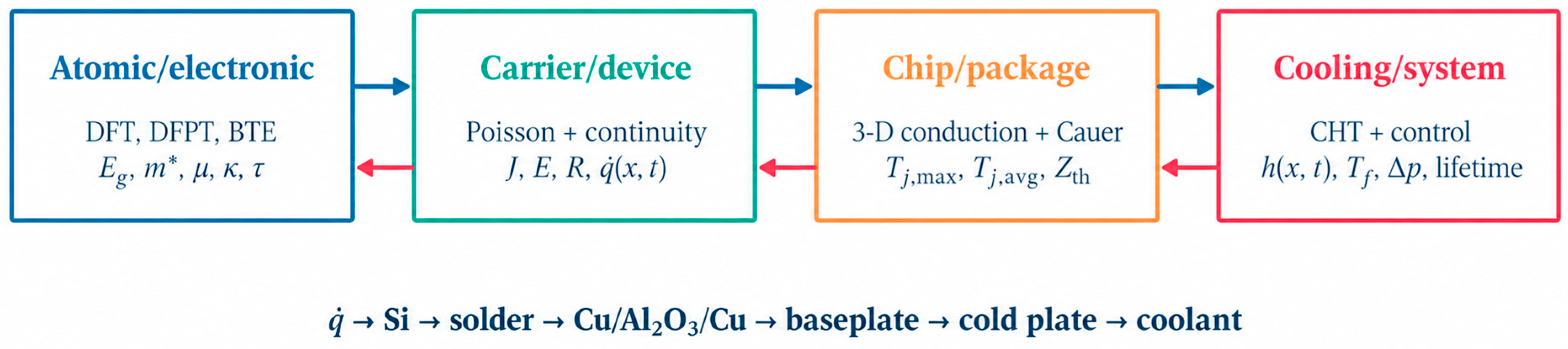
Figure 1. Multiscale hierarchy of heat generation and heat transfer in an IGBT module.
Applsci 16 09348 g001
Figure 2. Temperature–function interfaces from first-principles outputs to the device and thermal models.
Applsci 16 09348 g002
Figure 3. Atomic-scale lattice and phonon processes and their upscaling to device-level material functions.
Applsci 16 09348 g003
Figure 4. Micro-to-macro relationship among carrier motion, phonon transport, irreversible heat generation, package heat flow, and thermal feedback in an IGBT chip.
Applsci 16 09348 g004
Figure 5. Carrier injection, drift-region conductivity modulation, local dissipation, and formation of the IGBT turn-off tail current.
Applsci 16 09348 g005
Figure 6. Cross-scale temporal response of material functions, dynamic heat sources, thermal diffusion length, and package thermal memory.
Applsci 16 09348 g006
Figure 7. Junction-temperature and temperature-rise sensitivity to normalized carrier drift speed and an ion-migration/defect index.
Applsci 16 09348 g007
Figure 8. Layered IGBT package, heat-spreading angle, interfacial thermal resistance, and cold-plate boundary [25,26,27].
Applsci 16 09348 g008
Figure 9. Influence of phonon scattering, temperature, and a migration/defect index on silicon thermal conductivity and normalized chip-to-case thermal resistance.
Applsci 16 09348 g009
Figure 10. Cold-plate channels, spatial heat-transfer coefficient, and module-coolant energy boundary [29,30,31].
Applsci 16 09348 g010
Figure 11. Closed-loop coupling among electric field and carriers, heat sources, temperature, and stress or damage.
Applsci 16 09348 g011
Figure 12. Parameterized IGBT module geometry and local layered model.
Applsci 16 09348 g012
Figure 13. Local mesh refinement in the chip and solder layers and electrothermal-fluid boundary settings.
Applsci 16 09348 g013
Figure 14. Independent mesh-independence reconstruction: node count, maximum temperature, and relative error.
Applsci 16 09348 g014
Figure 15. Sequential and strongly coupled ANSYS/Fluent/Mechanical workflow.
Applsci 16 09348 g015
Figure 16. Independent parameterized equivalent-field calculation: three-phase chip heat sources, temperature field, and solder-layer stress derived from temperature and its gradient.
Applsci 16 09348 g016
Figure 17. Three-phase temperature field, interphase coupling, and boundary sensitivity from an independent two-dimensional diffusion reconstruction.
Applsci 16 09348 g017
Figure 18. Comparison between finite-element and theoretical Cauer layer temperatures under the two layerwise validation conditions.
Applsci 16 09348 g018
Figure 19. Periodic junction-temperature response with fixed and temperature-dependent loss in the Cauer model.
Applsci 16 09348 g019
Figure 20. Temperature gradient, constrained thermal stress, and damage-sensitivity fields constructed from the temperature field.
Applsci 16 09348 g020
Table 1. Scales, state variables, and transfer interfaces of the IGBT thermal problem.
Transfer to the Next ScaleHeat-Generation/
Transfer Characteristics
Governing EquationsLength/TimeScale
Eg, m*, μ, τ, κ, defect levelsElectron–phonon and defect scattering; no macroscopic temperature fieldKohn–Sham, DFPT, electron/phonon BTE0.1–10 nm; fs–psAtomic/electronic
q(x,y,z,t), Pcond, Eon/off/rrJ·E, recombination, avalanche, tail current, and reverse recoveryPoisson, continuity, drift-diffusion/bipolar transport0.1 micrometer-cm; ns–msCarrier/device
Tj,max, Tj,avg, Tj,J, Tj,sens, ∇T, Zth,ijEarly local diffusion, interlayer storage, lateral spreading, and multichip couplingNonlinear heat conduction, contact resistance, 3-D FE/Cauer0.1 mm–0.1 m; microseconds–10 sChip/package
h(x,t), Tf, σ, D, life consumptionConjugate heat transfer, flow distribution, coolant heating, and thermal fatigueNavier–Stokes, energy, thermoelastoplasticity, and damagecm–m; 0.1 s–hCooling/system
Table 2. Device-level mapping of atomic-scale and bulk-material parameters [22,23,24].
Upscaling Role and LimitationRepresentative Value/Temperature RangeParameter
Intrinsic concentration, leakage, and junction potential; Varshni relation or HSE/GW correction1.124 eV at 300 K; approximately 1.097 eV at 400 KBandgap Eg
Poisson equation and junction capacitance; calibrate high-field/frequency dependence as needed11.7 (Si, near room temperature)Relative permittivity εr
Mobility, density of states, and diffusivity; distinguish conductivity and DOS massesmc approximately 0.26 m0; DOS mass approximately 1.08 m0Electron effective mass
Valence-band transport; recalibrate under heavy doping and strainHeavy/light holes approximately 0.49/0.16 m0Hole effective mass
Prior for lightly doped bulk Si only; device regions require doping-, field-, and temperature-dependent correctionsμn approximately 1350, μp approximately 480 cm2/(V s) at 300 KLow-field mobility
Transient chip diffusion; interpolate the supplied material-property data148 at 300 K; 98.9 W/(m K) at 400 KLattice thermal conductivity κsi
Thermal diffusivity α = κ/(ρcp); determines penetration lengthρ = 2330 kg/m3; cp = 705–794 J/(kg K)Density/specific heat
Cannot be obtained from an ideal cell alone; calibrate using double-pulse, lifetime, or defect measurementsτHL, SRH level, and capture cross-sectionLifetime/defect parameters
Table 3. Layered material model of the IGBT module.
ρ (kg m−3)cp: 300–400 Kκ: 300–400 KThickness (mm)MaterialComponent
2330705–794148–98.90.08SiIGBT/FRD chip
731023554.80.08SnCuDie attach
8933384–397401–3930.30CuUpper DBC copper
375080024–200.32Al2O3DBC ceramic
8933384–397401–3930.30CuLower DBC copper
722023552.70.25Sn–SbDBC solder
8933384–397401–3933.0 *CuBaseplate
264088096.2As modeledADC12Heatsink/cold plate
* The baseplate thickness was set to 3.0 mm in the numerical model.
Table 4. Interfaces and time synchronization of the multiscale solvers.
Synchronization StrategyOutputInputModule
Offline synthesis and interpolation of published dataReference-calibrated Eg, m*, μ, κ, and τ functionsCrystal, defects, T, and strainPublished DFT/DFPT + BTE data (framework input; not independently solved)
ns-microseconds; period averagingPcond, Eon/off, q · (x,t)VGE, IC, Vdc, Tj, DDevice/circuit
microseconds-0.1 s; inner iterations when requiredTj,max, Tj,avg, Tj,J, ∇T, Q · Geometry, κ(T), ρcp, q · , h/TfElectrothermal FE
Thermal-cycle peaks/valleys or cycle jumpingσproxy and D* screening fieldsT(x,t), CTE, and viscoplastic parametersEquivalent-stress proxy (present study); calibrated Mechanical damage model (future)
0.01–1 s; two-way exchangePrescribed h(x,t), Tf, and Δp rangesMass flow rate, Tin, and wall heat fluxParameterized cold-side boundary (present study); two-way Fluent CHT (future)
0.1–10 msOnline T_j, pump speed, and life consumptionMission profile, sensors, and constraintsReduced order/control
Table 5. Cross-model difference metrics for the finite-element and Cauer calculations.
Mean Relative Difference, Three Cold-Side LayersMean Relative Difference, Four Chip-Side LayersSeven-Layer RMS DifferenceSeven-Layer Mean Absolute DifferenceCase
9.54%2.98%4.12 K3.61 KLC-1
12.56%1.28%9.27 K6.92 KLC-2
Disclaimer/Publisher’s Note: The statements, opinions and data contained in all publications are solely those of the individual author(s) and contributor(s) and not of MDPI and/or the editor(s). MDPI and/or the editor(s) disclaim responsibility for any injury to people or property resulting from any ideas, methods, instructions or products referred to in the content.