1. Introduction
Modern digital systems include a lot of different sequential devices [
1,
2]. Very often, to represent these devices, a model of a Mealy finite state machine (FSM) [
3] is used. An FSM model is a starting point for creating the electrical circuit of a sequential device. In this paper, we discuss a case where the circuits of Mealy FSMs are created using the internal resources of field-programmable gate arrays (FPGAs) [
4]. The choice of this basis is justified by the fact that FPGAs are a very popular tool used for creating the circuits of various digital devices [
5]. Moreover, FPGAs will be used in logic design within the next thirty years [
6].
As a rule, some optimization problems arise in the process of FSM design. These problems are interrelated. The following characteristics may require optimization [
7,
8,
9]: the amount of internal resources used (occupied chip area), or performance, or power consumption. In this article, we propose a method which allows for an increase in the maximum operating frequency of an FPGA-based Mealy FSM circuit. The following internal resources are used to create the circuit: look-up table (LUT) elements, programmable flip-flops, dedicated multiplexers, a synchronization tree, programmable interconnections and programmable input–outputs [
4,
8,
10]. We discuss a case where FSM states are encoded by composite state codes (CSCs) [
11]. This approach is based on creating groups of compatible states. Both groups and states are encoded using the minimum possible number of variables. The proposed method improves performance without a significant increase in the amount of internal resources used. We use the LUT count [
12] to estimate the chip area occupied by the FSM circuit.
Modern digital systems are processing larger and larger amounts of information [
13]. When implementing digital systems based on FPGAs, very often increasing the system performance without a significant increase in the amount of internal resources consumed is a problem [
14]. At the same time, the bottleneck may be the digital system control device, implemented in the form of an FSM. The control device generates control signals at each point in the system’s operation. Therefore, the performance of this control FSM significantly affects the performance of the digital system as a whole [
15]. One of the ways to increase the performance of an FSM is a state assignment, which allows us to reduce the number of logical levels in the FPGA-based FSM circuit [
16,
17]. In this article, we propose a state assignment method allowing us to increase the FSM performance without a significant overhead regarding the internal resources used.
The main contribution of this paper is a novel approach improving the cycle time (the operating frequency) of LUT-based Mealy FSM circuits with composite state codes. The improvement is based on transforming the maximum binary codes of groups of compatible states into one-hot codes (OHCs). Within each group, states are encoded by maximum binary codes (MBCs). This approach leads to the development of a new architecture of an FSM circuit different from the architecture where OHCs are not used [
11]. The performance improvement is related to the absence of the need to use group codes in the function assembler block. This approach allows the performance to improve for rather complex FSMs. A positive feature of this approach is the total absence of an increase in the amount of the internal resources of the FPGA chip used. Moreover, the proposed approach leads to the creation of circuits with slightly fewer LUTs than their equivalent CSC-based counterparts.
The main idea of this article is as follows: the transformation of maximum binary group codes into one-hot codes allows for a decrease in the number of partial Boolean functions generated by LUTs from the first logic level of an FSM circuit. Obviously, the code transformation requires additional LUTs and programmable interconnections (these are overheads of the proposed method), but our new method provides a decrease in the number of LUTs in the circuit assembling partial Boolean functions. This may result in a reduction in the values of LUT counts compared to the equivalent CSC-based FSMs. Our research shows that this phenomenon takes place for the proposed method.
The article includes seven sections, the first of which is this brief Introduction.
Section 2 shows the peculiarities of implementing an FSM with LUTs. The analysis of FSMs with composite state codes is discussed in
Section 3. An FSM architecture based on the transformation of group codes is proposed in
Section 4.
Section 5 is devoted to a synthesis example.
Section 6 shows and analyzes the obtained experimental results. The paper also includes a Conclusion (
Section 7).
2. LUT-Based FSM Design
There are a lot of approaches used for representing the behavior of a Mealy FSM [
1]. The most common are state transition graphs (STGs) or state transition tables (STTs) [
18]. We use both tools to represent transitions between the states from the set
. The transitions depend on FSM inputs comprising the set
. During the transitions, some FSM outputs are generated from the set
. As follows from these sets, an FSM has
M internal states,
L external inputs and
N outputs. For each state,
, an STG (or an STT) shows which outputs are generated under the influence of FSM inputs [
1]. There are
H interstate transitions represented by either an STG or STT.
The first step of FSM synthesis is a state assignment [
19]. During the state assignment, the abstract states
are represented by some physical objects. These objects are binary codes,
, having
R bits. The state codes consist of bits corresponding to state variables combined into a set,
. Using an STT, it is possible to derive systems of Boolean functions (SBFs) representing a combinational part of an FSM circuit. The state codes
are stored in a state code register,
. The minimum width (the number of bits) is provided by so-called maximum binary codes. Their width (
R) is determined as [
1]
To change the content of the RG, three objects are used. These objects are input memory functions (IMFs), a pulse of initialization,
, and a pulse of synchronization,
. As a rule, the RG consists of D flip-flops [
1]. Due to this, the IMFs create a set,
. If
, then a code for the initial state
is loaded into the RG. If a certain edge of the pulse
arises, then the bits of the IMFs are repeated in the contents of the RG.
Using an initial STT (or STG) and state codes, it is possible to derive the following SBFs [
20]:
These SBFs determine the combinational part of an FSM circuit. Systems (
2) and (
3) determine a so-called P FSM [
14]. The combinational part is implemented using some logic elements. The peculiarities of these elements significantly influence the architecture of an FSM circuit [
7].
This paper is devoted to the design of FPGA-based FSMs. Modern FPGAs include a lot of LUTs, which are parts of configurable logic blocks (CLBs) [
21]. In this article, we target chips produced by AMD Xilinx [
4]. The CLBs from this company consist of LUTs, dedicated multiplexers and programmable flip-flops. Using multiplexers, it is possible to obtain a super-LUT having more inputs than a basic LUT. For example, there are
inputs in the basic LUT from the Virtex-7 family of FPGAs [
4,
22]. To show the number of inputs, we denote an LUT as
-LUT. Inside a single CLB, either two seven-LUTs or one eight-LUT can be created with the help of multiplexers. These super-LUTs (SLUTs) have practically the same delay as their six-input counterparts [
23]. If an SLUT must have an
, then the internal resources of several configurable blocks are used. But such big SLUTs are significantly slower than SLUTs created inside a single CLB [
23]. In this paper, we use the symbol
to show that a logic block is implemented using LUTs and other internal CLB resources.
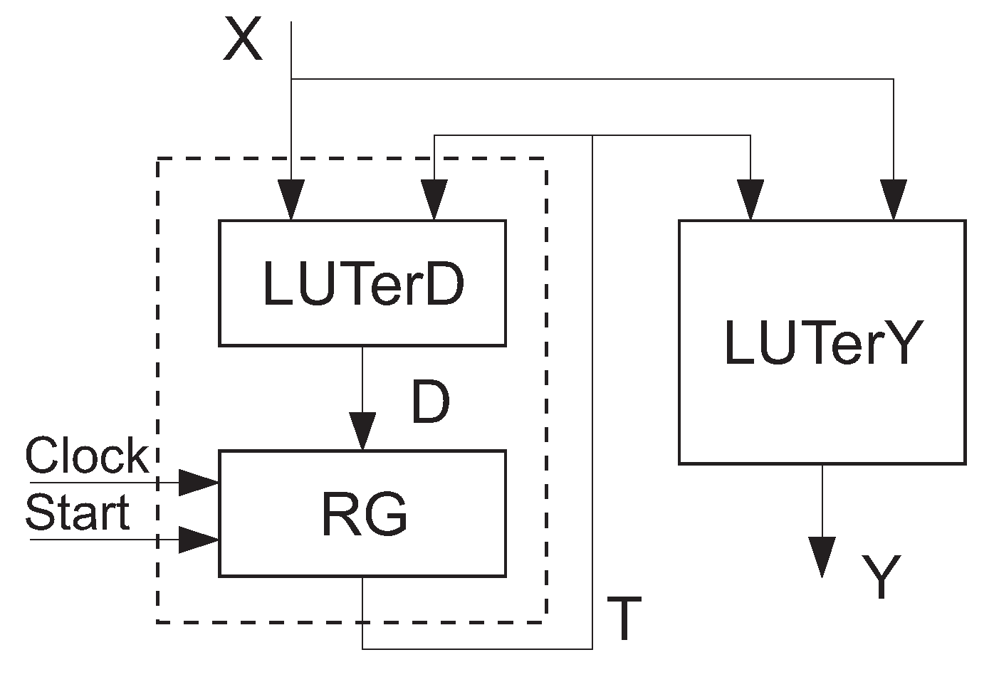
Because there is a direct connection between the outputs of LUTs and the inputs of flip-flops, such blocks are implemented as registers inside CLBs. So, the state code register is a part of an LUTer. This preliminary information allows for the creation of a structural diagram of the FPGA-based FSM
(
Figure 1).
A block,
, implements IMFs represented by the system (
2). We show the state register RG as a separate block, but in reality, this block is a part of
. The pulses
and
enter
. The FSM outputs (
3) are produced by the LUTs of the block
. These outputs are used by the other blocks of a digital system. So, it makes sense to reduce the delay between the arrival of FSM inputs,
, and the production of FSM outputs,
.
A serious drawback is inherent in modern FPGAs: the number of basic LUT inputs (
) is really small [
8]. This significantly affects the number of LUTs and their levels in the FSM circuit. If the sum of product (SOP) of a Boolean function,
, includes
literals, then the corresponding LUT-based circuit is multi-level if
To construct the SOPs of functions
, it is necessary to create a direct structure table (DST) [
20]. Both STGs and STTs could be used for constructing a DST [
18]. In our paper, we start synthesis using an STG.
An STG includes M vertices corresponding to FSM states. The vertices are connected by arcs determining interstate transitions. There are H arcs in an STG. The arc number is determined by the values of and . The conjunction of inputs is an input signal determining a particular transition. The symbol stands for a collection of outputs (CO) generated during a particular transition.
To create a DST, it is necessary to transform an STG into the equivalent STT. An STT includes the following columns: (the current state), (a state of transition), (an input signal), (a collection of outputs), and h (the number of interstate transitions). The first column includes the current state, the second column contains a state of transition, the third column contains an input signal determining the transition from the current state into the next state, and a CO generated during the transition, , is written in the fourth column.
A DST is an extension of the original STT with three additional columns. Two of the additional columns contain binary codes,
and
. The third column includes a collection of IMFs,
, determining the code
[
20]. Of course, there are the same number of rows in the equivalent STT and DST.
Two types of codes are typical for FSMs: maximum binary codes and one-hot codes [
24]. These approaches have both positive and negative aspects. Using MBCs leads to the minimum possible number of flip-flops into the RG, but this leads to really complex SOPs for functions (
2) and (
3). As a result, an FSM circuit may include a lot of LUT levels and a very sophisticated system of interconnections [
7]. One-hot codes are characterized by having the maximum number of bits (
). This leads to the use of many more flip-flops than in the case of MBC-based FSMs, but the SOPs of the IMFs and FSM outputs are rather simple.
A comparison of FSMs based on MBCs and OHCs was executed in article [
25]. This comparison showed that using OHCs provides better results for FSMs with
. As was shown in [
3], both LUT counts and power consumption depend significantly on the value of
L. The following conclusion can be made from an analysis of the experiments conducted by the authors of paper [
26]: MBC-based FSMs have better characteristics (as compared with OHC-based FSMs) if the following condition holds:
.
If condition (
4) is true for a function,
, then this function should be decomposed. In this case, such a function is represented by a collection of partial Boolean functions (PBFs). To find such a representation, methods of functional decomposition (FD) [
27] could be applied. To be represented by a single-LUT circuit, any partial function should depend on no more than
arguments. Next, all LUTs generating partial Boolean functions representing the same function,
, should be combined into a multi-level circuit. It is known that applying FD-based methods results in multi-level FSM circuits having a very complicated system of interconnections [
28,
29].
To increase the value of the operating frequency, it is necessary to reduce the number of logic levels in an FPGA-based FSM circuit. This could be achieved, for example, by reducing the number of literals in the sum of products representing IMFs and FSM outputs. One of the ways used to solve this problem is an optimal state assignment [
28]. The well-known algorithm JEDI [
30] is the best example of such an approach’s efficiency. Optimization is achieved due to the placement of some state codes into the generalized cubes of an
R-dimensional Boolean space. These cubes include the maximum binary codes of states for which transitions depend on the same input signals,
. To minimize the corresponding SOPs, it is necessary to use adjacent codes for these states. Moreover, this goal may be achieved by increasing the number of bits in the state codes. This leads to FSM circuits having fewer LUTs, LUT levels and interconnections than equivalent FSM circuits based on other state assignment methods. Basing on the results shown in [
31], we should point out that applying JEDI leads to an improvement in LUT counts, performance and power consumption.
3. Peculiarities of FSMs Based on Composite State Assignment
Composite state assignment is proposed in paper [
11]. As follows from [
11], using CSCs may improve the main characteristics of FPGA-based FSM circuits: the resulting circuits occupy a smaller chip area and provide a higher operating frequency than their counterparts based on MBCs, OHCs and JEDI.
To execute the composite state assignment, it is necessary to split the set of states
A by
groups of compatible states,
. This leads to a partition,
, with the minimum possible number of groups. The groups
are encoded by maximum binary codes,
, with
bits:
The groups are encoded using elements of the set
.
Maximum partial state codes encode states
inside each group,
. If a group,
, includes
elements, then the width of the partial codes is determined as
To create partial state codes,
variables are necessary. The value of
is determined as
The partial state variables determine the set
. So, the total number of group and partial state variables,
, is determined as
Expression (
8) also determines the number of IMFs generated (and the number of flip-flops in the RG).
The concatenation of codes
and
determines a composite state code,
, of the state
. So, the composite state codes are determined by the following expression:
In (
9), we use the symbol ∗ to show the concatenation of two binary vectors.
To implement a CSC-based FSM circuit, it is necessary to find three sets representing each group, . The partial set of inputs includes inputs determining transitions from the states . This set includes elements. The partial set of outputs includes FSM outputs, , generated during transitions from the states . The set of IMFs includes input memory functions generated during transitions from the states .
Each group,
, should satisfy the following condition:
To create the partition
, it is possible to use the method proposed in [
32]. This approach allows us to find a partition,
, with the minimum possible number of groups,
.
So, each group determines the following PBFs:
To obtain the final values of functions
, it is necessary to assemble the corresponding partial functions. This is achieved using group codes. Each partial function should be multiplied by a conjunction,
, corresponding to the code
. So, the final values of SBFs (
2) and (
3) are determined by the following systems:
As shown in [
11], the functions (
13) and (
14) could be generated using the dedicated multiplexers of CLBs [
23,
33].
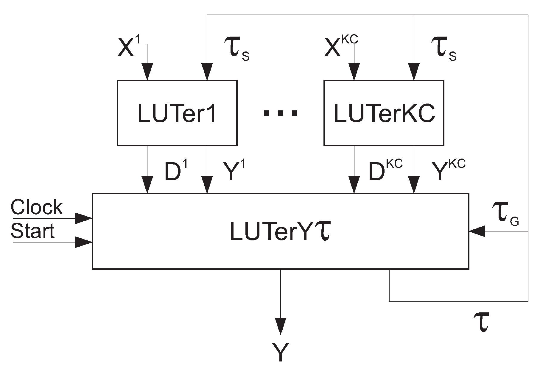
So, there should be two levels of logic blocks in the circuit of the CSC-based Mealy FSM
. The architecture of this circuit is determined by systems (
11)–(
14). The architecture of FSM
(
Figure 2) is proposed in article [
11].
In FSM
, LUT-based blocks,
–
, form the first logic level of the FSM circuit. The block
generates partial functions (
11) and (
12), representing the group
. The function assembler is represented by the block
. The function assembler generates functions (
13) and (
14). The FSM outputs (
14) enter the other blocks of the digital system. The IMFs (
13) enter the flip-flops of the register RG. The outputs of the flip-flops determine both the group and partial state codes.
In [
11], the results of various experiments are shown. The experiments allowed for a comparison of the characteristics of CSC-, MBC- and OHC-based FSMs. These results show that CSC-based FSMs have better LUT counts than are obtained using either MBCs or OHCs. It is very important that reducing the LUT count does not reduce the values of the maximum operating frequencies.
The best case for using CSC-based FSMs was determined in [
11]. These conditions are the following:
If condition (
15) is violated, then practically, there is no need to use FD-based approaches. The corresponding FSM circuits are mostly single-level [
11]. If condition (
16) is true, then there is a single level of LUTs in the function assembler circuit. If both conditions (
15) and (
16) hold, then there are two levels of LUTs in the circuits of
-based FSMs.
As follows from the analysis of systems (
13) and (
14), the violation of condition (
16) is connected with the existence of a direct dependence between the functions
and group variables
. So, to reduce the number of levels in the function assembler circuit, it is necessary to eliminate this direct dependence. This will allow for the deletion of the conjunctions
from functions generated by the function assembler. One of the possible approaches for solving this problem is proposed in our current article.
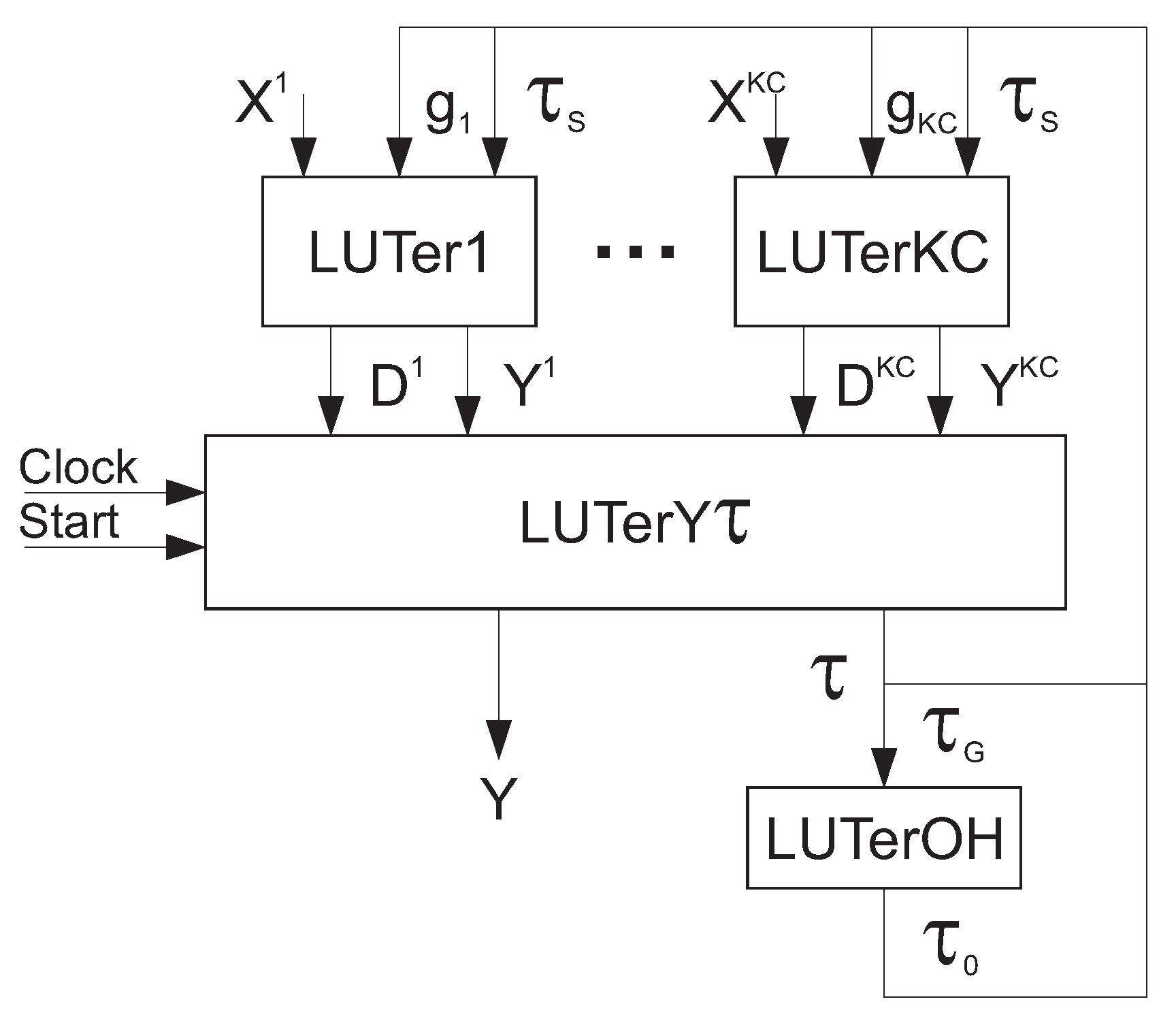
4. The Main Idea of the Proposed Method
In this paper, we propose a method aimed at the relocation of group variables from to blocks from the first logic level. This diminishes the number of arguments in functions . In turn, this increases the probability of obtaining a single-level circuit for the block . We propose encoding the groups using one-hot codes. The states are still encoded by maximum binary partial codes. Now, the groups are encoded using the elements of the set . These variables enter the blocks –. This means that the variable determines a literal used by all the PBFs generated by the LUTs of the block . This method is focused on a situation where a single-level implementation of the function assembler circuit is impossible.
Now, the variables determining the one-hot group codes should enter the LUTs of the blocks
–
. This leads to a change in equations for both PBFs and full functions. Now, the LUTs of the first logic level generate the following SBFs:
In this case, there are no connections between the group codes and LUTs of
. This leads to the following SBFs representing the function assembler:
Now, the IMFs in (
19) are used to create the composite state codes. In these codes, groups are represented by maximum binary codes. To create the one-hot group codes, it is necessary to transform these maximum group codes into their one-hot equivalents. The transformation is executed by an additional code transformer block. The code transformer generates the following system of functions:
We name the resulting state codes mixed composite state codes (MCSCs). The term “mixed” means that the groups are represented by OHCs and the partial state codes are maximum codes. The proposed approach leads to the development of the MCSC-based Mealy FSM
. Its architecture is shown in
Figure 3.
In an MCSC-based FSM, SBFs (
17) and (
18) are generated by the LUTs of the first logic level. These LUTs create the blocks
. The LUTs of block
generate the final values of the FSM outputs
and input memory functions. The block
generates the SBF (
21). As a result, one-hot group codes are created.
The block includes the hidden state code register. This register is controlled by IMFs, together with signals and . Obviously, the equivalent FSMs and have the same amount of flip-flops in the RG. The outputs of the RG are variables from the set .
The block
is a code transformer. It turns maximum binary group codes into the corresponding one-hot group codes. This block is based on an SBF (
21).
To create the partition
, we use the greedy algorithm proposed in [
34]. The compatible states are found using condition (
10). As follows from Equations (
17) and (
18), it is necessary to reserve one of LUT inputs for a corresponding one-hot group variable. Obviously, this can lead to the necessity of using more than a single basic LUT for implementing a circuit for a partial Boolean function. So, it is possible that more LUTs would be necessary on the first logic level than there are for the equivalent FSM
.
Let, for each group,
, the SOP of any partial function,
, depend on
literals. Let the following condition apply:
In this case, including the variable
in any SOP does not lead to the development of a multi-level circuit. Obviously, if condition (
22) is violated, then the function
is represented by a multi-LUT circuit.
To diminish the number of CLBs required for implementing partial functions,
, it makes sense to encode some states,
, using the adjacent partial codes
. This may be performed using, for example, a method similar to that of the algorithm JEDI [
30].
For a better understanding of the novelty of the proposed method, it is necessary to show the main difference between the proposed method of state assignment and one-hot state assignment. One-hot codes include the maximum possible number of bits. This leads to a simplification of input memory functions due to a significant increase in the number of flip-flops used (compared to this number for FSMs using MBCs). An increase in the number of memory elements leads to an increase in the number of interconnections, which can significantly increase the FSM cycle time [
16]. The method we propose allows for obtaining state codes where the number of bits is practically the same as for maximum binary codes. This allows for an increase in the FSM performance compared to the performance of equivalent OHC-based FSMs.
In this paper, we propose a synthesis method for the LUT-based Mealy FSM . The synthesis process starts with an STG. The proposed method includes the following steps:
Transforming the initial STG into a state transition table.
Creating the partition of the set of states with the minimum number of groups.
The encoding of groups using maximum binary codes, .
The encoding of groups using one-hot codes, .
The encoding of states using partial state codes, .
Creating composite state codes, .
Creating tables of blocks –.
Deriving SBFs (
17)–(
18), representing the circuits of
–
.
Creating a table for block .
Creating a table for block
and an SBF (
21).
Implementing the FSM circuit using the resources of a particular FPGA chip.
5. Example of Synthesis of Mealy FSM
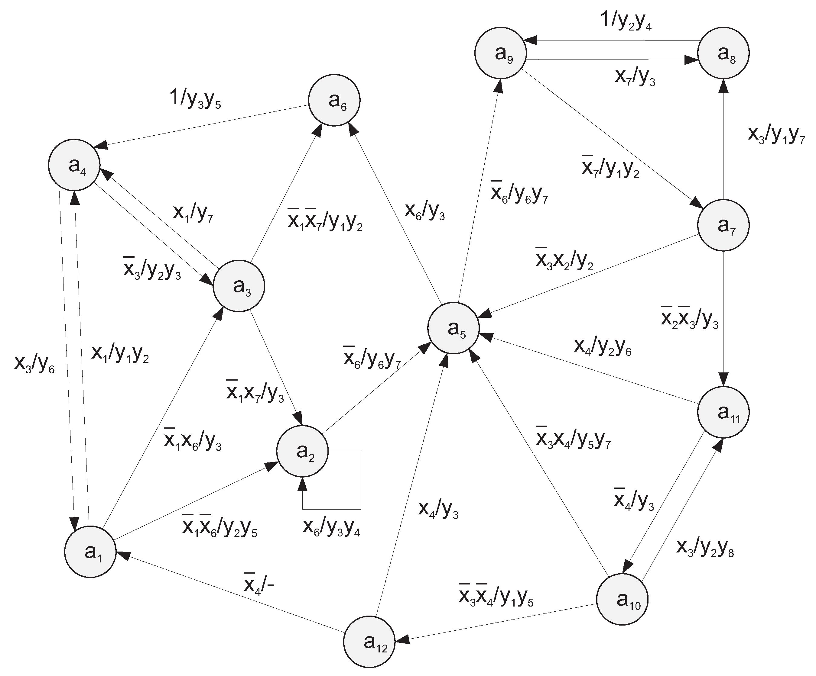
Let us discuss an example of synthesis based on the proposed method. We applied this method to synthesize an LUT-based circuit for FSM A1. To obtain the circuit, we used LUTs with six inputs. The behavior of FSM A1 is represented by a state transition graph, shown in
Figure 4.
Step 1. An analysis of
Figure 4 shows that FSM
has the following characteristics:
,
,
and
. This determines the sets
,
and
. Using approach [
18], we can transform the STG (
Figure 4) into the equivalent STT with
rows (
Table 1).
Each arc of the STG represents the pair of vertices
. The
hth row of the STT corresponds to the
hth arc of the STG. The columns of the STT include the following variables:
is the current state (the arc’s beginning);
is a state of transition (the arc’s end);
is an input signal written above the
hth arc (it determines the transition from
into
);
is a collection of outputs written above the
hth arc
;
h is the number of transitions
. The transition from an STG to the equivalent STT is transparent and straightforward [
18].
Step 2. This step is executed using the greedy algorithm proposed in [
34]. We have
. Applying the method from [
34] gives us the partition
with
.
The states
are distributed among the groups in the following way:
,
and
. So, for each group, we have
. The group
determines the partial sets
and
. The group
determines the partial sets
and
. The group
determines the partial sets
and
. Using (
6), we can obtain
. Using (
7), we can obtain the value
. We have
for each group,
. Taking into account variables
, we can find that a single LUT with six inputs is enough to generate any partial function.
Step 3. We have
. Using (
5), we can obtain
. This determines the set
. Now, we can form the set
. There is no influence of the group codes on the number of LUTs in the blocks
–
. Due to this, we can encode the groups in the following way:
,
and
.
Step 4. Obviously, three bits is enough to create the one-hot group codes. This determines the set . Let us encode the groups in the following way: , and .
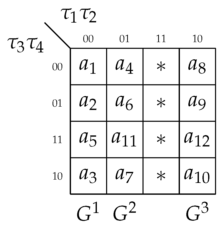
Step 5. In complex FSMs, it makes sense to encode states using the algorithm JEDI for optimal state encoding. This can lead to the optimization of the partial SOPs for output functions.
But in this very simple example, we encode states in the basic way. The method is the following: the smaller the subscript of a state, the more zeros its partial code includes. Using this approach, we can assign the following partial codes (
Figure 5).
Step 6. In the Karnaugh map (
Figure 5), we show these partial codes together with the maximum binary group codes. So, this map shows the composite state codes.
So, steps 1–6 are executed. Using the obtained codes, we can create tables representing the blocks LUTer1–LUTer3.
Step 7. In the discussed case, LUTer1 is represented by
Table 2, LUTer2 by
Table 3, and LUTer3 by
Table 4. These tables have the columns
,
,
,
,
,
,
and
h. For each state, the columns
,
,
and
are the same as they were in the initial STT (
Table 1). The column
is created using the composite state codes from
Figure 5.
Step 8. The outcome of the previous step provides information which can be used for creating the SOPs of partial IMFs (
13) and partial microoperations (
14). This is performed using the partial state codes, inputs
and one-hot group variables. There are two stages in creating PBFs. The first stage is deriving the partial Boolean functions (
11) and (
12) from the tables of blocks LUTer1–LUTerKC. The second stage is multiplying each term of SOPs (
11) and (
12) by the corresponding one-hot group variables. So, the PBFs representing
are multiplied by
. The resulting expressions represent SBFs (
13) and (
14).
For our example, we show only the SOPs resulting from the partial functions
and
,
and
, and
and
. These partial SOPs are represented by the following equations:
In these systems, variables
are product terms created from the lines,
h, of tables representing blocks LUTer1–LUTerKC. We hope there is a transparent connection between SBFs (
23) and (
24) and
Table 2,
Table 3 and
Table 4.
Step 9. To obtain the final values of both the IMFs and FSM outputs, it is necessary to create a table for the function assembler. This is a table for the block
. The table contains
rows. This table provides information about the disjunctions of PBFs. Using this information, the final values of the FSM outputs and IMFs are obtained. There are the following columns in this table:
, 1, …,
. The row number
i includes the function
. The column number
k corresponds to the partial function
. If the function
is generated by the block
, then there is a value of 1 at the intersection of the column
k and row
i. Otherwise, the symbol 0 is written at this intersection. In the discussed case, the block
is represented by
Table 5.
Step 10. Using
Table 5 allows us to obtain a system of disjunctions representing functions
. In the discussed case, some IMFs are represented by SBF (
25), and some outputs are represented by SBF (
26):
Obviously, using a similar approach, we can obtain the SOPs of all the functions from SBFs (
19) and (
20).
Step 11. To construct SBF (
21), it is necessary to create a table for the block
. This table includes the columns
,
,
,
and
k. In the discussed case, the code transformer is represented by
Table 6.
The following SBF is derived from
Table 6:
As follows from SBF (
27), there is only a single LUT in the circuit of
. The variables
and
are exactly the same as group variables
and
, respectively.
Step 12. To implement the FPGA-based circuit, it is necessary to apply some industrial CAD tools. These tools are necessary to execute the technology mapping [
3,
35]. The most popular tools are Vivado [
36] and Quartus [
37]. We do not discuss this step for our example.
To analyse the efficiency of the proposed approach compared to some other known methods, we conducted a lot of experiments. We compared the characteristics of -based FSMs with the characteristics of their counterparts based on maximum binary state codes, one-hot state codes and composite state codes. In the next section, we show the results of our experiments and their analysis.
6. Experimental Results
We conducted experiments to compare four characteristics of
-based FSM circuits with the characteristics of FSM circuits based on other state assignment methods. These characteristics were the cycle times, maximum operating frequencies, LUT counts and area–time products. As an example of an MBC-based method, we use Vivado’s Auto method [
36]. Let us point out that the number of code bits used by Auto may exceed the minimum value determined by (
1). Vivado’s one-hot method [
36] was used as an example of OHC-based state assignment. Also, we compared our approach with the algorithm JEDI [
30], which is an MBC-based algorithm creating cubes covering the codes of some states [
3]. Finally, we executed a comparison of
-based FSM circuits with their
-based counterparts [
11].
In the experiments, we used benchmark FSMs from the well-known library LGSynth93 [
38]. There are 48 Mealy FSMs (benchmarks) in the library. The benchmarks are represented in the KISS2 format. These benchmarks have a wide range of basic characteristics (numbers of states, inputs, outputs and transitions). A lot of scientists have been using these benchmarks as a basis for the comparison of various design methods [
39,
40,
41]. The characteristics of the benchmarks are shown in
Table 7. The last column of this table includes the sum of the number of FSM inputs and the minimum number of bits in the maximum binary state codes. We used this additional column to select benchmarks where structural decomposition made sense.
To conduct the experiments, we used a platform including the FPGA chip from the Virtex-7 family. This was a VC709 Evaluation Platform (xc7vx690tffg1761-2) [
22]. The CLBs used included basic LUTs with six inputs
. To implement a CLB-based circuit of
, the dedicated multiplexers could be used. Each CLB included four basic LUTs and three dedicated multiplexers. We use thed industrial CAD package Vivado v2019.1 (64-bit) [
36] to execute the step of technology mapping. Using the Vivado reports, we created four tables showing the results of the conducted experiments.
Each Boolean function,
, depended on
arguments. If condition (
4) was violated for all IMFs and FSM outputs, then the circuit of FSM
consisted of exactly
LUTs. So, each function,
, was generated by a single-level circuit. In this case, the
-based FSM circuit possessed the best spatial and temporal characteristics. This model provided the minimum values of the LUT count and propagation time. So, if condition (
4) is violated for all input memory functions and FSM outputs, there is no need to use either functional or structural decomposition. Obviously, the states may be encoded in a way minimizing the power consumption [
24,
27].
As follows from the results of the experiments shown in article [
11], condition (
4) only held for some benchmarks. These benchmarks had the following common property:
For FSMs satisfying (
28), it made sense to replace
-based FSMs with FSMs with composite state assignment. We could use either the
or
models. For FPGAs from the Virtex 7 family, the basic LUT had
inputs. Due to this, in our research, we only used benchmarks for which
. The experimental results are shown in
Table 8 (cycle times, nanoseconds),
Table 9 (maximum operating frequency, MHz),
Table 10 (LUT counts) and
Table 11 (area–time products).
Table 8,
Table 9,
Table 10 and
Table 11 include the following columns: FSM (names of benchmark FSMs); MB (experimental results for MBC-based FSMs); OH (experimental results for OHC-based FSMs); JEDI (experimental results for FSMs with state codes generated by JEDI);
(experimental results for FSMs with composite state codes); and
(experimental results obtained for our new approach). The results of the summation of values from the corresponding columns are shown in the row “Total”. The row “Percentage” shows the percentage of the summarized characteristics of the investigated FSM circuits compared to those of
-based FSMs.
The main goal of the proposed method was increasing the performance of LUT-based FSM circuits in relation to the circuits of FSMs based on composite state codes. So, the most important characteristic was the cycle time (or operating frequency). The values for the cycle times were obtained directly from Vivado reports. These values are shown in
Table 8.
As follows from
Table 8, the proposed method made it possible to obtain LUT-based FSM circuits with shorter cycle times than those of the other studied FSMs. As can be seen from
Table 8,
-based FSMs had the following improvements in cycle times: (1) 82.25% compared with MBC- based FSMs; (2) 84.37% compared with OHC-based FSMs; (3) 60.28% compared with JEDI-based FSMs; and (4) 8.81% compared with
-based FSMs.
An analysis of
Table 8 shows that under some conditions, our method always produced circuits that were slightly faster than the circuits of the equivalent FSMs with composite state codes, but the level of improvement depended on the value of
. For example, we found
for the benchmark
. As follows from
Table 8, our method provided an improvement of around 1%. Next, we found
for the benchmark
. As follows from
Table 8, our method provided an improvement of around 19%. As we compare the results for each benchmark, we can make the following conclusion: the improvement achieved by replacing composite state codes with mixed CSCs increased with the growth of the value
.
We think that this phenomenon was related to the difference in the number of CLBs connected in series in the circuit creating the input memory functions and outputs of Mealy FSMs. As the value of increased, the number of consecutive CLBs grew faster for CSC-based FSMs than for the equivalent MCSC-based FSMs.
Using the values for the cycle time allowed us to create
Table 9. This table shows the values of the maximum operating frequencies.
As follows from
Table 9, the proposed method produced FPGA-based FSM circuits with higher frequencies than the other studied FSMs. As can be seen from
Table 9,
-based FSMs achieved the following improvements in the frequency: (1) 45.2% compared with Auto-based FSMs; (2) 55.49% compared with OHC-based FSMs; (3) 37.44% compared with JEDI-based FSMs; and (4) 7.89% compared with
-based FSMs. The reasons for this state of affairs have already been considered in the analysis of the data from
Table 8. We will not repeat them.
The main goal of the proposed approach is to improve the temporal characteristics of LUT-based FSM circuits in relation to the circuits of the equivalent CSC-based FSMs, but sometimes, it is very important that an increase in the frequency does not result in a significant deterioration of the spatial characteristics. These characteristics depend significantly on the number of LUTs used (LUT count) [
12]. A comparison of the values of the LUT counts for FSM circuits based on various state assignment methods is shown in
Table 10.
As follows from
Table 10, the proposed approach led to the creation of FSM circuits that required fewer LUTs than the other investigated methods. Our method had an average improvement of (1) 55.06% compared with Auto-based FSMs, (2) 68.35% compared with OHC-based FSMs, (3) 26.12% compared with JEDI-based FSMs, and (4) 4% compared with FSMs based on composite state codes.
Sometimes, it is very important to reach a balance between the spatial and temporal characteristics of FSM circuits [
19]. This balance can be estimated using some integral evaluations of the quality of a digital circuit. One of the main integral evaluations involves the product of the area occupied by a circuit and its performance (area–time product) [
12]. In the case of LUT-based circuits, the area is estimated using a characteristic such as the LUT count [
12]. Obviously, the performance is represented by the value of the cycle time. The smaller the value of this integral characteristic is, the higher the quality of the circuit (and the better the balance between the spatial and temporal characteristics). Using Vivado reports, we created
Table 11, including values of the area–time products obtained for the circuits of the benchmark FSMs.
As follows from
Table 11, the proposed method made it possible to obtain LUT-based FSM circuits with smaller values for the area–time products compared with their
-based counterparts. The
-based FSMs were inferior in relation to the equivalent
-based FSMs (the difference was 12.19%). Also, our method provided significantly better results than those for the other methods studied. The improvement was 189.39% in relation to MB-based FSMs, 216.87% in relation to OH-based FSMs and 104.06% in relation to JEDI-based FSMs.
An analysis of the results of the experiments carried out allowed us to draw the following conclusion regarding the equivalent
- and
-based FSMs. If condition (
28) holds, then our method is always an improvement over the method based on composite state codes [
11]. Under this condition, our method provides a shorter cycle time and requires fewer LUTs than the method based on CSCs. So, mixed composite state codes can be viewed as a good alternative to maximum binary CSCs.


