Article

Filtered Operator-Based Nonlinear Control for DC–DC Converter-Driven Triboelectric Nanogenerator System

by
Ryusei Shimane
,
Chengyao Liu
and
Mingcong Deng
*
Department of Electrical Engineering and Computer Science, Tokyo University of Agriculture and Technology, 2-24-16 Nakacho, Koganei-shi 184-0012, Tokyo, Japan
*
Author to whom correspondence should be addressed.
Appl. Sci. 2025, 15(7), 4054; https://doi.org/10.3390/app15074054
Submission received: 22 February 2025 / Revised: 31 March 2025 / Accepted: 4 April 2025 / Published: 7 April 2025

Abstract

:
In recent years, with the growing interest in the Internet of Things (IoT) and decarbonization, energy harvesting has been attracting attention. Energy harvesting is a technology that converts ambient energy such as light, heat, and vibration into electrical power, and it is also known as environmental power generation. A triboelectric nanogenerator is a type of energy harvesting device that converts mechanical energy, such as vibration, into electrical energy using the triboelectric effect and electrostatic induction. The advantages of this device include low cost and high durability. Due to the principle of triboelectric nanogenerators, a stable output voltage cannot be obtained, so auxiliary circuits such as DC–DC converters are required to obtain the desired voltage. In this paper, a DC–DC converter is utilized, controlled by a system based on operator theory, with a filter incorporated to enhance tracking performance, ensuring that the output voltage follows the target value.

1. Introduction

In recent years, energy harvesting has been attracting attention along with the growing interest in IoT and a low-carbon society. Energy harvesting is a technology used to convert the energy around us, such as light, heat, and vibration, into electric power. By enabling the conversion of currently unused energy into electrical energy, it is expected to enhance overall energy efficiency. Furthermore, in the field of IoT, numerous sensors are utilized. By harvesting energy from ambient sources to power these sensors, it becomes possible to eliminate the need for battery replacement and power supply wiring, thereby reducing maintenance costs. Triboelectric nanogenerators (TENGs) are a type of energy harvesting device that convert mechanical energy, such as vibrations and friction, into electrical energy by leveraging the triboelectric effect and electrostatic induction [1]. The triboelectric effect is a phenomenon where electric charges move and materials become electrified due to the repeated contact and separation of two different types of materials. TENGs operate based on several distinct modes [2,3,4]. The most representative operating modes include the following: In the Vertical Contact–Separation Mode, electrical charges are transferred upon the contact of two different materials, and, as they separate, a potential difference is generated between the electrodes, causing the charge to flow through an external circuit for power generation. In the Sliding Mode, friction between two materials sliding against each other results in the transfer of charges and the generation of a potential difference, leading to the flow of charge through an external circuit. In the Single-Electrode Mode, electricity is generated through the movement of charges between a single electrode and a grounded object, such as the human body. Finally, in the Freestanding Triboelectric-Layer Mode, two stationary electrodes are arranged on the same plane, and an independent dielectric layer moves between them to generate power. They can generate electrical power not only from the vibrational energy of structures, such as iron bridges and buildings, but also from subtle and diverse energy sources, including the mechanical impact of falling raindrops, the low-velocity water flow in oceans and waterways, and the frictional interaction between snow and shoe soles during ambulation on snowy surfaces [5,6,7]. The advantages of these devices include their low cost, high durability, and the ability to convert low-frequency vibrations into electrical power [8,9,10]. Although triboelectric nanogenerators have not yet found specific applications, certain research reports have indicated successes in powering a stopwatch [11]. Furthermore, TENGs are not only utilized as power sources but are also expected to be applied as self-powered mechanical sensors by leveraging their ability to convert mechanical energy into electrical energy [12]. In fact, research is being conducted on their use as force sensors. However, due to the inherent principles of TENGs, it is not possible to achieve a constant output voltage [13]. Certain TENGs have been developed with structures designed to output a constant voltage; however, due to their structural characteristics, their applications are limited [14]. Power management circuits using PUTs and thyristors have also been studied, but while these circuits can maintain a constant output voltage, they are unable to achieve the desired voltage [15]. Therefore, regulators such as DC–DC converters are required to obtain the desired voltage. A DC–DC converter circuit includes switching elements such as FETs, and by varying the state of these switching elements using pulse-width modulation (PWM) signals, the output voltage is also adjusted. Several attempts have been made to control the output voltage of power generation elements, such as the thermoelectric generators used in energy harvesting, whose output voltage is not constant, using DC–DC converters [16,17].
The output current of TENGs is extremely small, requiring consideration of the discontinuous conduction mode (DCM), where the current flowing through the inductor of the DC–DC converter becomes discontinuous [18]. Furthermore, DC–DC converters operating in DCM exhibit nonlinear characteristics, making precise control difficult. A buck converter, as used in this research, is a type of DC–DC converter that exhibits linearity in continuous conduction mode (CCM) but demonstrates nonlinearity in DCM. Typically, when constructing control systems for nonlinear control objects, the control object is linearized to apply linear control theory. However, this linearization can potentially degrade the performance of the control system in terms of response speed, tracking accuracy, and sensitivity to characteristic variations [19]. Therefore, research on the robust design of control objects exhibiting nonlinearity is being conducted. While H-infinity control and Sliding Mode control are widely recognized as nonlinear control theories [20,21], in this paper, the control system is constructed using operator theory, which is a type of nonlinear control theory [22,23]. Sliding Mode control has the drawback of chattering behavior and the challenge of designing an appropriate sliding surface, which is attributed to the difficulty in finding a suitable Lyapunov function for nonlinear systems [24,25]. However, a control system based on operator theory has the advantage of not having these drawbacks. In the proposed control system, target value tracking is enabled by combining right coprime factorization based on operator theory with a low-pass filter [26]. By controlling a buck converter, which outputs a voltage lower than the input voltage in the designed control system, the output voltage of the triboelectric nanogenerator is adjusted to obtain the desired voltage.
The structure of this paper is as follows: In Section 2, the operating principle of the Vertical Contact–Separation Mode TENG used in this study is discussed. In Section 3, a mathematical model of a buck converter compatible with DCM for controlling the output voltage of the TENG is presented. In Section 4, a control system based on operator theory is designed. In Section 5, the results of simulations and real experiments are presented. Finally, Section 6 concludes the paper.

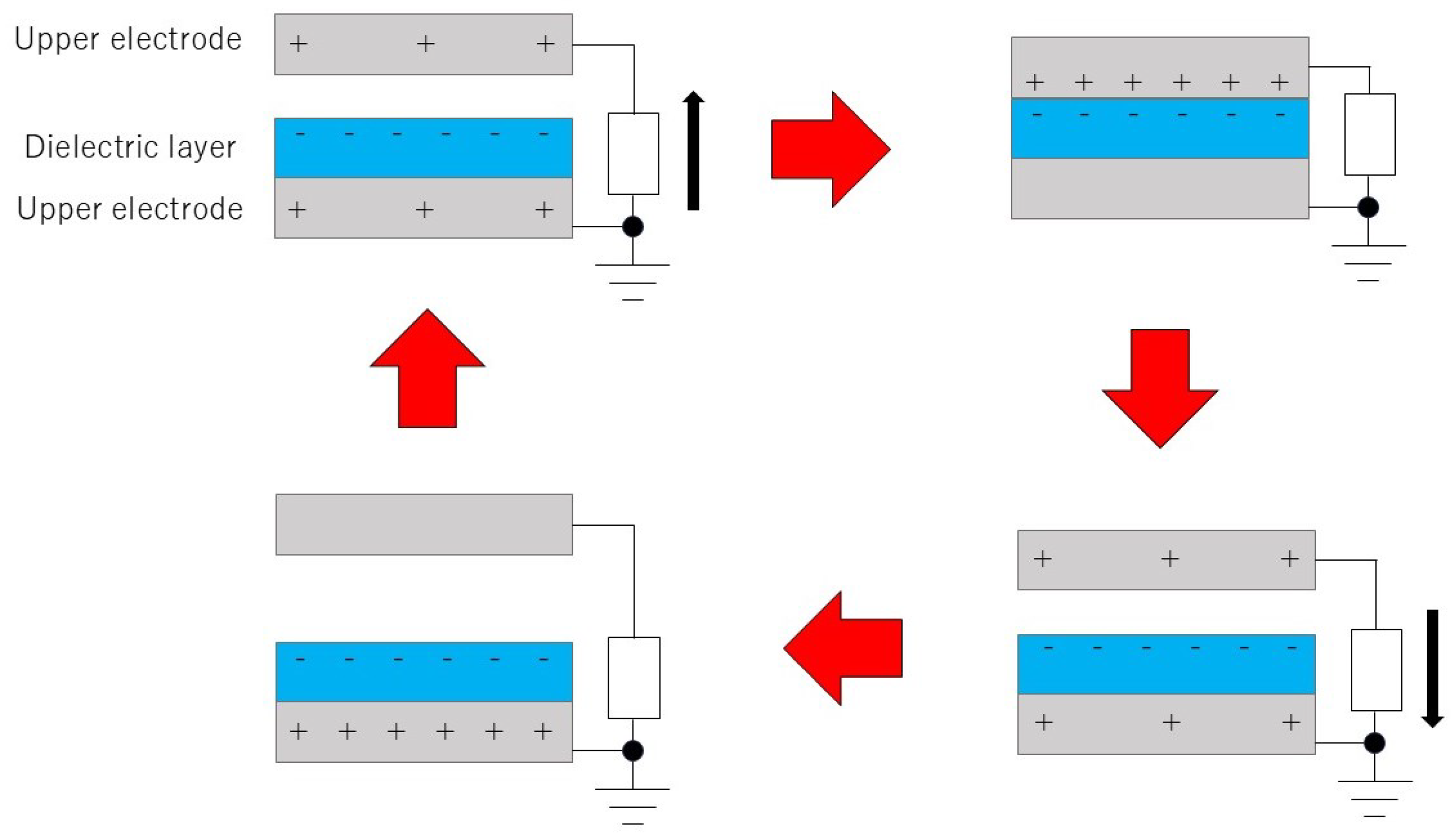
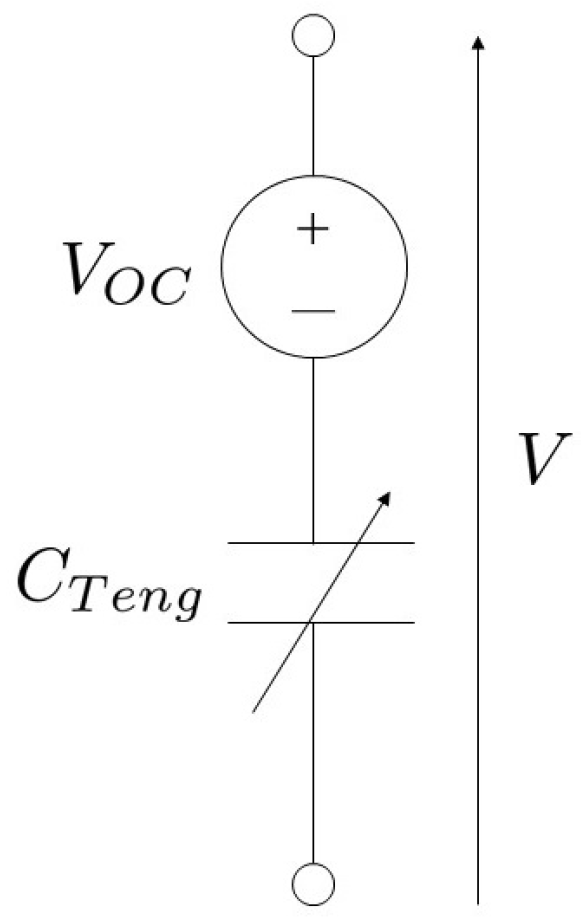
2. Operating Principle of the TENG

The TENG used in this study operates in the Vertical Contact–Separation Mode and consists of one or two dielectric layers and electrodes, generating electricity by utilizing the triboelectric effect and electrostatic induction. In the case where there is only one dielectric layer, the dielectric layer is in direct contact with the electrode, leading to charge transfer. When there are two dielectric layers, charge transfer occurs through the contact between the dielectrics. The fundamental operation of devices with one dielectric layer and those with two dielectric layers is the same. Here, the operation is explained using an example with a single dielectric layer. The operation of the TENG in the Vertical Contact–Separation Mode is illustrated in Figure 1.
When the dielectric layer and the electrode come into contact due to vibrations or other mechanical forces, charge transfer occurs, resulting in one surface becoming positively charged and the other becoming negatively charged. The quantity and polarity of the generated charges depend on the properties of the dielectric material. After contact, as the dielectric layer and the electrode separate, the opposing positive and negative charges create an electric field in the surrounding space. To neutralize the resulting potential difference, a current flows from one electrode to the other until the potentials of both electrodes equalize. When the dielectric layer and the electrode approach each other again, the potential difference induced by the charge pair decreases, causing the current to flow in the direction opposite to the separation phase. By repeating this process of contact and separation periodically, an alternating current is continuously generated [27].
The equivalent circuit of the triboelectric nanogenerator is presented in Figure 2.
The voltage arising from charging and the electrostatic capacitance between the electrodes are defined as V O C ( x ( t ) ) and C T e n g ( x ( t ) ) , respectively. Furthermore, V O C ( x ( t ) ) is expressed by Equation (1), and C T e n g ( x ( t ) ) is given by Equation (2):
V O C ( x ( t ) ) = σ x ( t ) ε 0
C T e n g ( x ( t ) ) = S ε 0 d 0 + x ( t )
where ε 0 represents the electric constant, and its value is 8.854 × 10 12 . d 0 is the thickness of the dielectric layer, and its unit is mm . x ( t ) denotes the distance between the dielectric layers, and its unit is m . S is the area of the electrode, and its unit is m 2 . σ is the surface charge density, and its unit is C / m 2 .
The terminal voltage V of the TENG is expressed by Equation (3):
V = Q C T e n g ( x ( t ) ) + V O C ( x ( t ) )
where Q is the moving charge quantity, and its unit is C .

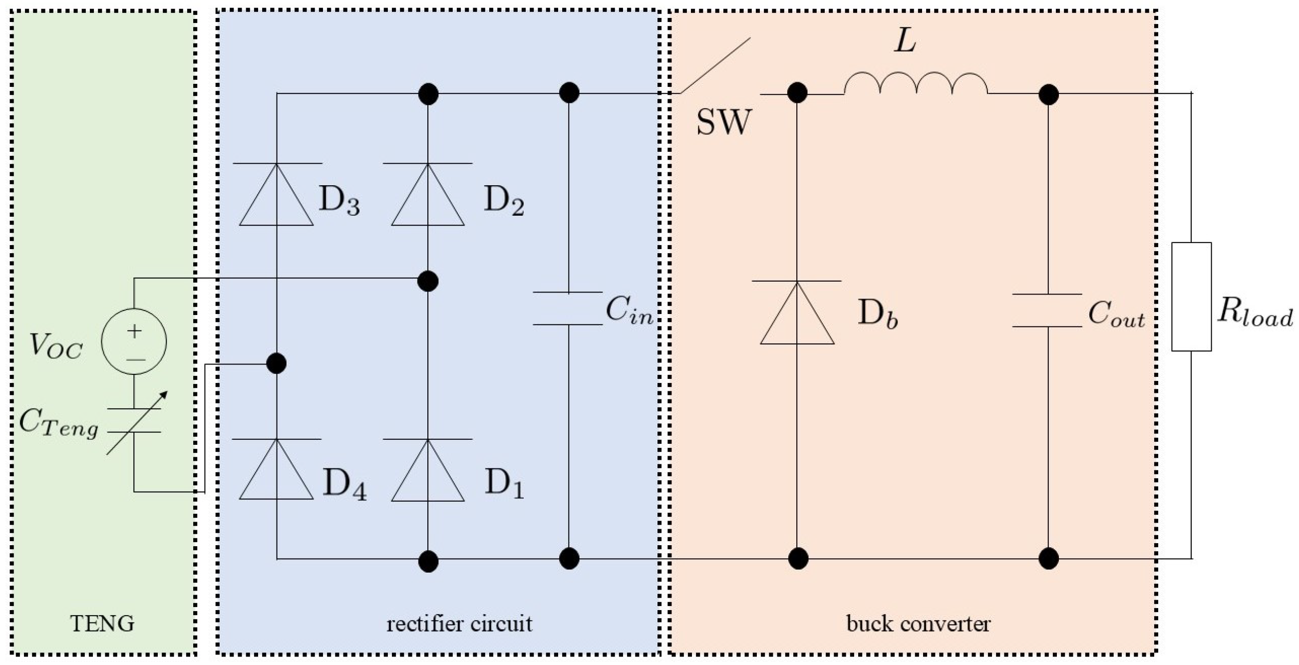
3. Modeling of the TENG System
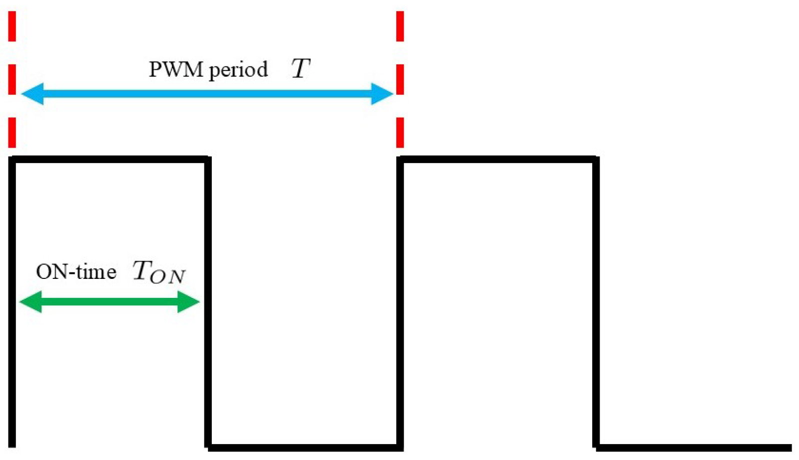
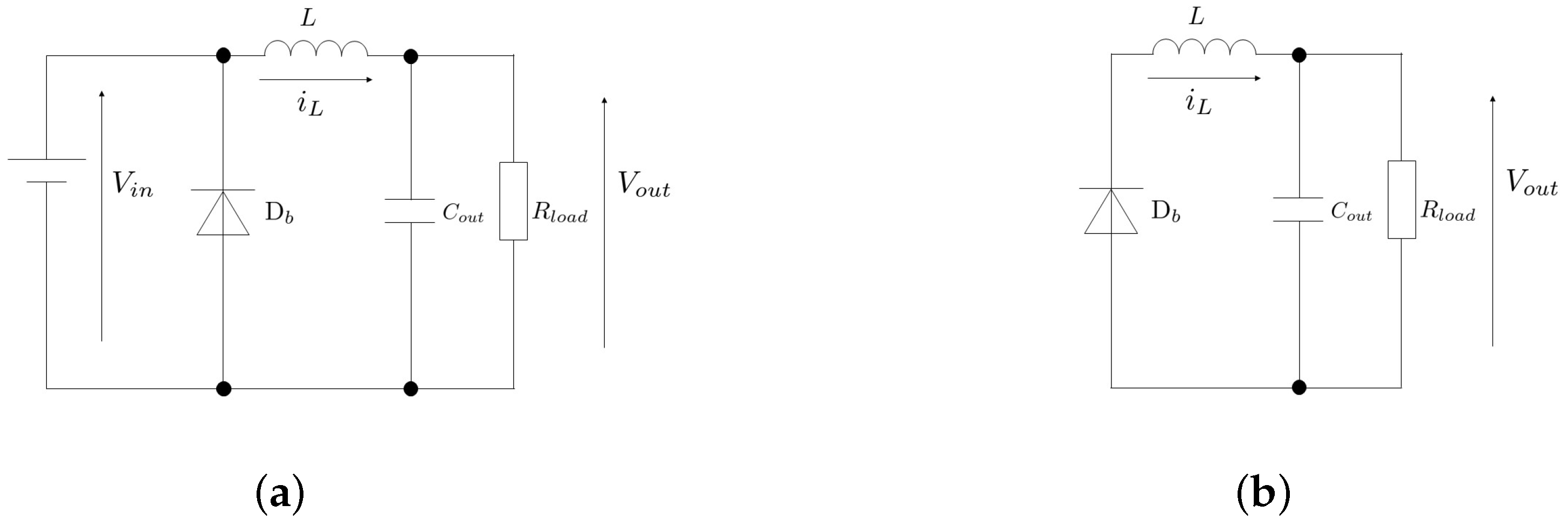
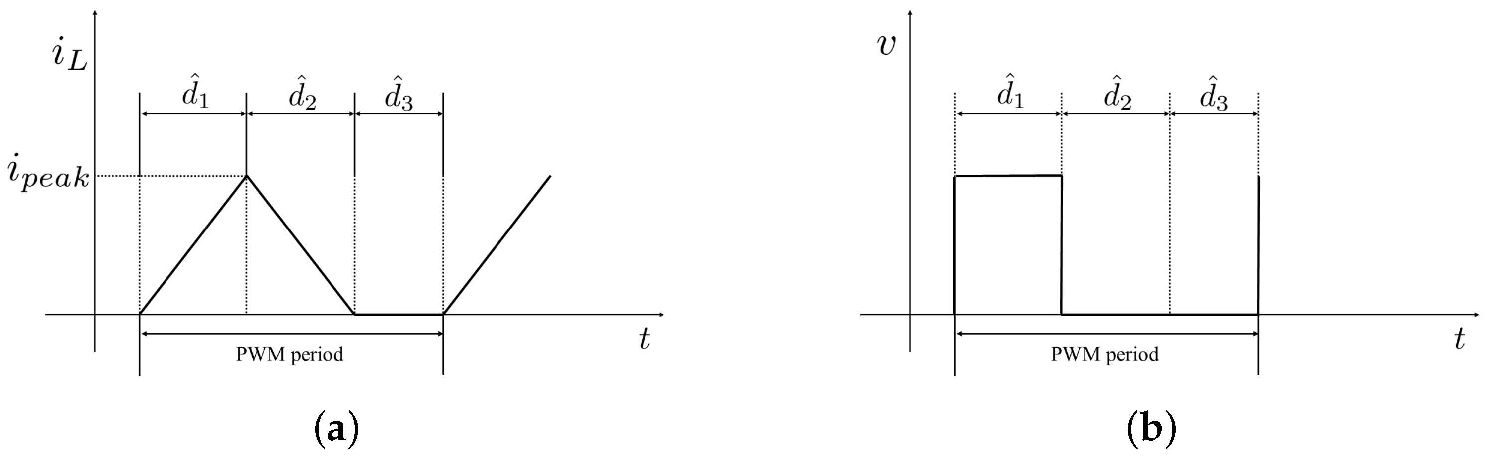
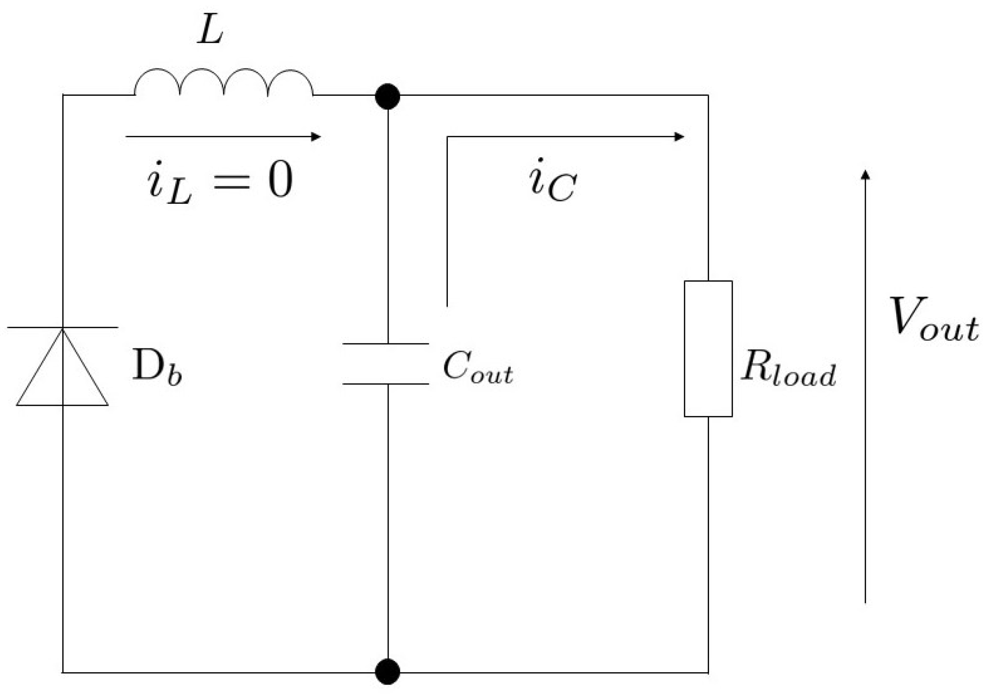
3.1. Buck Converter

In this research, a buck converter (a type of DC–DC converter) is used to control the TENG’s output voltage. In Figure 3, the buck converter circuit is connected to the rectifier circuit to obtain a steady output voltage. The buck converter can produce a voltage lower than the input voltage. The DC–DC converter operates in two states: ON and OFF. The switch state is controlled by a pulse-width modulation (PWM) signal. The duty cycle, defined as the ratio of ON time to the PWM period, is given in Equation (4). Here, T is the pulse period, and T O N is the pulse width.
d ^ = T O N T
The parameters for the buck converter are as follows: V i n represents the input voltage, and its unit is V . V o u t is the output voltage, and its unit is V . i L denotes the inductor current, and its unit is A . The load resistance is denoted by R l o a d , and its unit is Ω . L is the inductance, and its unit is H . Additionally, C o u t refers to the output capacitor, and its unit is F .
In this research, the widely applicable state-space averaging method (WASAM) is used for modeling, as it accommodates both CCM and DCM [28]. As it is first necessary to obtain a model using the state-space averaging method, the modeling process begins with this approach. For DC–DC converters, the system is modeled separately for each state, where the switch is either ON or OFF and weighted based on the PWM duty cycle (Figure 4). By superimposing these weighted models, an averaged model of the DC–DC converter can be obtained.
In Figure 5, the circuit equation for the equivalent circuit in the ON state is expressed by Equation (5):
d i L d t = 1 L V o u t + 1 L V i n d V o u t d t = 1 C o u t i L 1 R l o a d C o u t V o u t
Similarly, the circuit equation for the equivalent circuit in the OFF state is expressed by Equation (6):
d i L d t = 1 L V o u t d V o u t d t = 1 C o u t i L 1 R l o a d C o u t V o u t
By weighting and superimposing the circuit equations for the ON and OFF states, expressed in Equations (5) and (6), respectively, with the duty cycle d, the model equation for the DC–DC converter is derived. The obtained model equation is presented in Equation (7):
d i L d t = 1 L V o u t + d ^ L V i n d V o u t d t = 1 C o u t i L 1 R l o a d C o u t V o u t
For CCM, modeling using the above method is sufficient; however, for DCM, additional characteristics must be taken into consideration. Figure 6 illustrates the characteristics in DCM, where the inductor current consists of three intervals: charging ( d ^ 1 ) , diode conducting ( d ^ 2 ) , and discontinuous ( d ^ 3 ) intervals. The duty cycle of the charging interval is d ^ 1 , which corresponds to the on time within a PWM period. The duty cycles of the diode conducting and discontinuous intervals are d ^ 2 and d ^ 3 , respectively, satisfying the relationship d ^ 1 + d ^ 2 + d ^ 3 = 1 .
The circuit configuration varies across different intervals. During the charging interval d ^ 1 , the switch is turned on, and the current through the inductor increases linearly. The circuit configuration at this time is shown in Figure 5a. In the diode conducting interval d ^ 2 , the switch is off, while the diode is on, and the current decreases linearly until it reaches zero. This state’s circuit configuration is depicted in Figure 5b. During the discontinuous interval d ^ 3 , both the switch and the diode are off, and the output circuit consists solely of the capacitor and the load. The circuit configuration for this interval is illustrated in Figure 7. In DCM, it is necessary to consider the state shown in Figure 7 in addition to the states shown in Figure 5a,b for modeling. While it is theoretically possible to weight and superimpose these three states, accurately measuring the rapidly fluctuating inductor current within a short period is not practical. Therefore, modeling using the conventional state-averaging method is difficult.
In DCM, the inductor current becomes completely zero, leading to the occurrence of ringing. Due to this ringing, high-frequency components are also present in the inductor current. Here, assuming that the inductor current contains both a low-frequency component i L L and a high-frequency component i L H , the inductor current i L can be expressed as follows:
i L = i L L + i L H
The average current of i L H per switching cycle can be expressed by Equation (3) as follows, where T S W is the switching period:
i L H = d ^ T S W ( V i n V o u t ) 2 L
In the WASAM, the inductor current i L is modeled by substituting it with the aforementioned low-frequency component i L L and high-frequency component i L H [28]. When the state variables are i L L and V o u t , the model equations can be expressed as in Equation (10):
d i LL d t = V o u t L + d ^ V i n L d V o u t d t = i L L C o u t 1 R l o a d C o u t + d ^ T S W 2 L C o u t V o u t + d ^ T S W 2 L C o u t V i n

3.2. Problem Statement

The power supply for general electrical devices and sensors is required to provide a stable DC output voltage. Due to the fundamental principle of triboelectric nanogenerators, achieving a constant output voltage is challenging; therefore, a DC–DC converter is utilized to obtain the desired output voltage. To compensate for the stability of a nonlinear control system that considers the nonlinearity of DCM, a control system based on operator theory is designed. Furthermore, applying right coprime factorization in combination with a low-pass filter ensures accurate tracking of the target value.

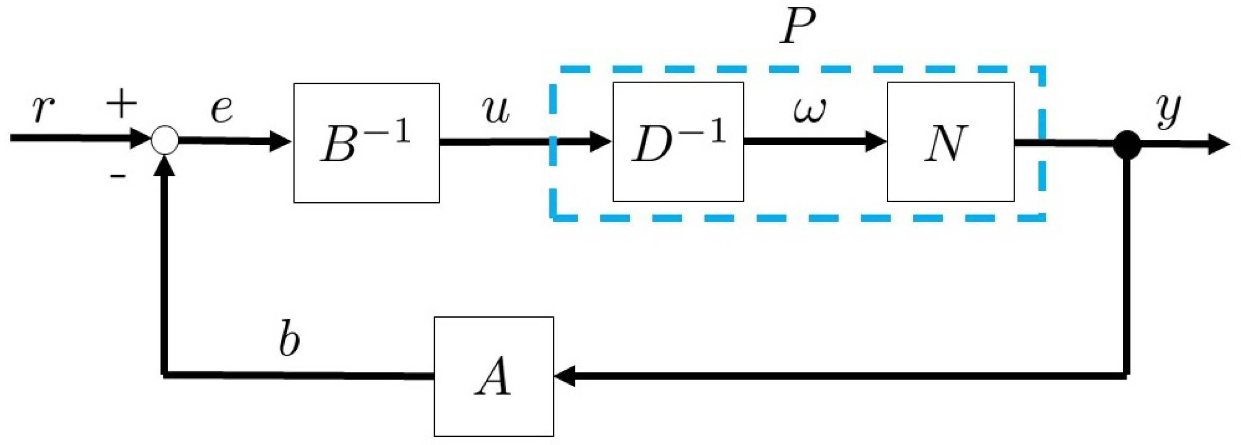
4. Control System Design

4.1. Right Factorization

Control systems are designed using operator theory, which allows for handling systems in the time domain without linearization and compensates for the BIBO stability of nonlinear control targets. First, right factorization is performed. The right factorization is illustrated in Figure 8. As shown in Figure 8, P : U Y is a plant, which is a DC–DC converter in this research. U represents the input space, and Y represents the output space. Additionally, W is referred to as a quasi-state space. When the plant P : U Y is factorized as shown in Equation (11) using a stable operator N : W Y and a stable and invertible operator D : W U , this factorization is called right factorization.
P = N D 1
Next, the concept of filtered right factorization is explained. Define the internal state signal space within the plant as W ˜ , and assume the existence of a stable operator N ˜ : W ˜ Y and a stable and invertible operator D ˜ : W ˜ U . Here, N ˜ and D ˜ constitute the right factorization of P. Next, consider a stable operator Q : W W ˜ . Using the operator Q, we define the operators N and D as N = N ˜ Q : W Y and D = D ˜ Q : W U [29]. Considering the right factorization after passing through the operator Q, we obtain the following equation:
P = N D 1 = ( N ˜ Q ) ( Q 1 D ˜ 1 ) = N ˜ D ˜ 1
From Equation (12), the results of the right factorization remain unchanged, even when using operators filtered through a filter. A block diagram illustrating this right factorization is shown in Figure 9.
Thus, by designing an appropriate operator Q, various characteristics can be imparted to the control system. In this research, the operator Q is designed to have low-pass filter characteristics, thereby enabling accurate tracking of the reference value.

4.2. Operator Theory

In this section, right coprime factorization and control system design based on operator theory utilizing this factorization are discussed. The operators A : Y U and B : U U are designed to satisfy the Bézout identity, as shown in Equation (13). Both A and B are stable, and B is invertible. When the Bézout identity is satisfied, the operators N and D are referred to as the robust right coprime factorization of the plant P. Additionally, M : W U is a unimodular operator [30].
A N + B D = M
Figure 10 illustrates the control system based on operator theory. The operators N, D, A, and B need to be designed to satisfy the Bezout identity given by Equation (13). In Figure 10, r represents the reference value, u denotes the plant input, ω is the quasi-state, y is the plant output, b indicates the feedback signal, and e represents the error.
The design of the control system based on operator theory is undertaken. Plant P ( u ) ( t ) is represented by Equation (14). The variables x 1 and x 2 correspond to i L L and V o u t in Equation (10), respectively. Additionally, the duty cycle is considered as the control input u ( t ) .
P : d x 1 ( t ) d t = 1 L x 2 ( t ) + u ( t ) L V i n d x 2 ( t ) d t = 1 C o u t x 1 ( t ) u ( t ) T S W 2 L C o u t + 1 R l o a d C o u t x 2 ( t ) + u ( t ) T S W 2 L C o u t V i n y ( t ) = x 2 ( t )
From Equation (14), we factorized the plant P into D ˜ 1 and N ˜ on the right side. The designed N ˜ and D ˜ 1 are shown in Equations (15) and (16), respectively.
N ˜ : y ( t ) = V i n ω ˜ ( t )
D ˜ 1 : d x d 1 ( t ) d t = 1 L x d 2 ( t ) + u ( t ) L V i n d x d 2 ( t ) d t = 1 C o u t x d 1 ( t ) u ( t ) T S W 2 L C o u t + 1 R l o a d C o u t x d 2 ( t ) + u ( t ) T S W 2 L C o u t V i n ω ˜ ( t ) = 1 V i n x d 2 ( t )
Furthermore, from Equation (16), D ˜ is expressed as follows:
D ˜ : x d 2 ( t ) = V i n ω ˜ ( t ) d x d 1 ( t ) d t = 1 L x d 2 ( t ) + u ( t ) L V i n u ( t ) = 2 L T S W ( V i n x d 2 ) C o u t d x d 2 ( t ) d t x d 1 ( t ) + x d 2 ( t ) R l o a d
The operator Q is designed to function as a low-pass filter. Here, τ represents the time constant of the low-pass filter. The operator Q is shown in Equation (18):
Q : d ω ˜ ( t ) d t = 1 τ ω ˜ ( t ) + ω ( t )
Furthermore, the operators N and D are designed as operators passed through the low-pass filter Q, as shown in Equations (19) and (20), respectively.
N : d ω ˜ n ( t ) d t = 1 τ ω ˜ n ( t ) + ω ( t ) y ( t ) = V i n ω ˜ n ( t )
D : d ω ˜ d ( t ) d t = 1 τ ω ˜ d ( t ) + ω ( t ) x d 2 ( t ) = V i n ω ˜ d ( t ) d x d 1 ( t ) d t = 1 L x d 2 ( t ) + u ( t ) L V i n u ( t ) = 2 L T S W ( V i n x d 2 ) C o u t d x d 2 ( t ) d t x d 1 ( t ) + x d 2 ( t ) R l o a d
The unimodular operator M is designed as shown in Equation (21):
M : r ( t ) = V i n ω ( t )
By transforming Equation (13), the following equation is obtained:
B = ( M A N ) D 1
The operator B, designed based on Equation (22), is presented in Equation (23). Here, the operator A is assumed to be the identity operator.
B : d b 1 ( t ) d t = 1 L b 2 ( t ) + u ( t ) L V i n d b 2 ( t ) d t = 1 C o u t b 1 ( t ) u ( t ) T S W 2 L C o u t + 1 R l o a d C o u t b 2 ( t ) + u ( t ) T S W 2 L C o u t V i n b b ( t ) = b 2 ( t ) d x b 1 ( t ) d t = 1 L x b 2 ( t ) + u ( t ) L V i n d x b 2 ( t ) d t = 1 C o u t x b 1 ( t ) u ( t ) T S W 2 L C o u t + 1 R l o a d C o u t x b 2 ( t ) + u ( t ) T S W 2 L C o u t V i n ω ˜ b ( t ) = 1 V i n x b 2 ( t ) r b ( t ) = V i n τ d ω ˜ b ( t ) d t + ω ˜ b ( t ) e ( t ) = r b ( t ) b b ( t )
From Equation (23), the operator B 1 is expressed as shown in Equation (24):
B 1 : r b ( t ) = e ( t ) + b b ( t ) d b 1 ( t ) d t = 1 L b 2 ( t ) + u ( t ) L V i n d b 2 ( t ) d t = 1 C o u t b 1 ( t ) u ( t ) T s w 2 L C o u t + 1 R l o a d C o u t b 2 ( t ) + u ( t ) T s w 2 L C o u t V i n b b ( t ) = b 2 ( t ) d ω ˜ b ( t ) d t = 1 τ ω ˜ b ( t ) + r b ( t ) V i n x b 2 ( t ) = V i n ω ˜ b ( t ) d x b 1 ( t ) d t = 1 L x b 2 ( t ) + u ( t ) L V i n u ( t ) = 2 L T S W ( V i n x b 2 ) C o u t d x b 2 ( t ) d t x b 1 ( t ) + x b 2 ( t ) R l o a d

4.3. Proof of Stability of Control System

In operator theory, stability is guaranteed by satisfying the Bezout identity. First, we demonstrate A N and B D using Equations (19), (20) and (23).
A N : d ω ˜ n ( t ) d t = 1 τ ω ˜ n ( t ) + ω ( t ) b ( t ) = V i n ω ˜ n ( t )
B D : d ω ˜ d ( t ) d t = 1 τ ω ˜ d ( t ) + ω ( t ) x d 2 ( t ) = V i n ω ˜ d ( t ) d x d 1 ( t ) d t = 1 L x d 2 ( t ) + u ( t ) L V i n u ( t ) = 2 L T S W ( V i n x d 2 ) C o u t d x d 2 ( t ) d t x d 1 ( t ) + x d 2 ( t ) R l o a d d b 1 ( t ) d t = 1 L b 2 ( t ) + u ( t ) L V i n d b 2 ( t ) d t = 1 C o u t b 1 ( t ) u ( t ) T S W 2 L C o u t + 1 R l o a d C o u t b 2 ( t ) + u ( t ) T S W 2 L C o u t V i n b b ( t ) = b 2 ( t ) d x b 1 ( t ) d t = 1 L x b 2 ( t ) + u ( t ) L V i n d x b 2 ( t ) d t = 1 C o u t x b 1 ( t ) u ( t ) T S W 2 L C o u t + 1 R l o a d C o u t x b 2 ( t ) + u ( t ) T S W 2 L C o u t V i n ω ˜ b ( t ) = 1 V i n x b 2 ( t ) r b ( t ) = V i n τ d ω ˜ b ( t ) d t + ω ˜ b ( t ) e ( t ) = r b ( t ) b b ( t )
If all internal state initial values are 0 and ω ˜ = ω ˜ n = ω ˜ d = ω ˜ b , then from Equation (18), r b is expressed as follows.
r b ( t ) = V i n ω
Furthermore, assuming b ( t ) = b b ( t ) ,
e ( t ) + b ( t ) = r b ( t )
From Equations (27) and (28), it can be seen that the Bezout identity in Equation (13) holds.

5. Simulation and Experiment

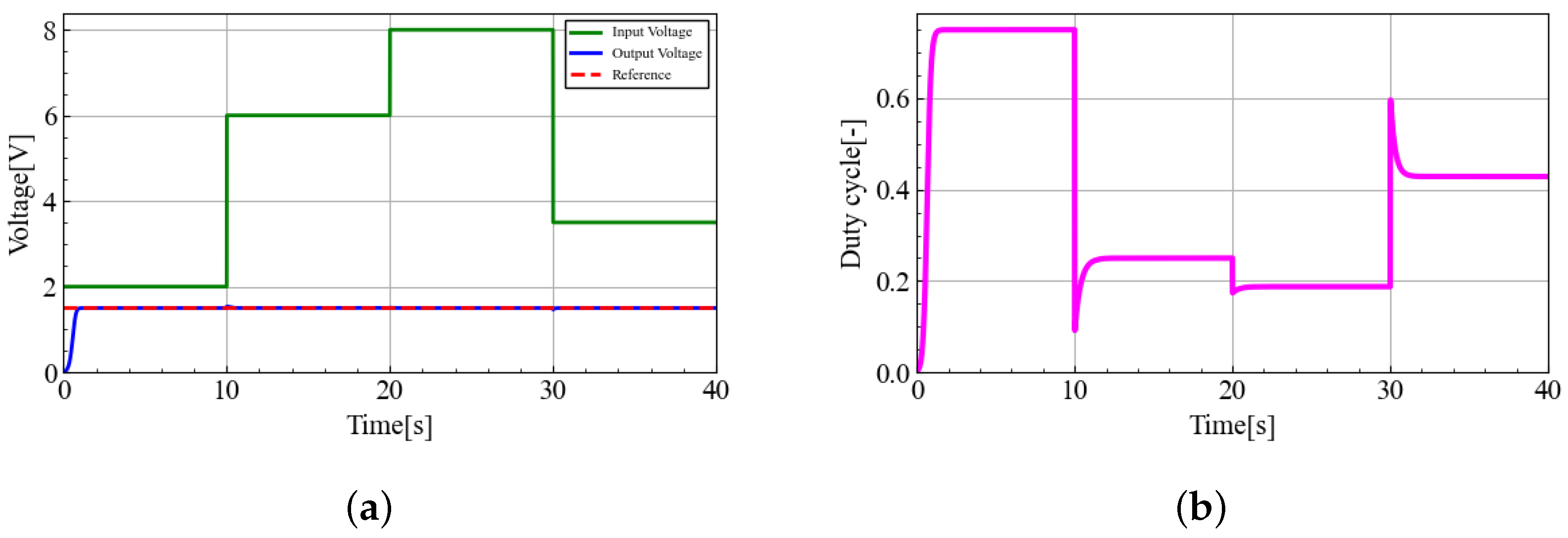
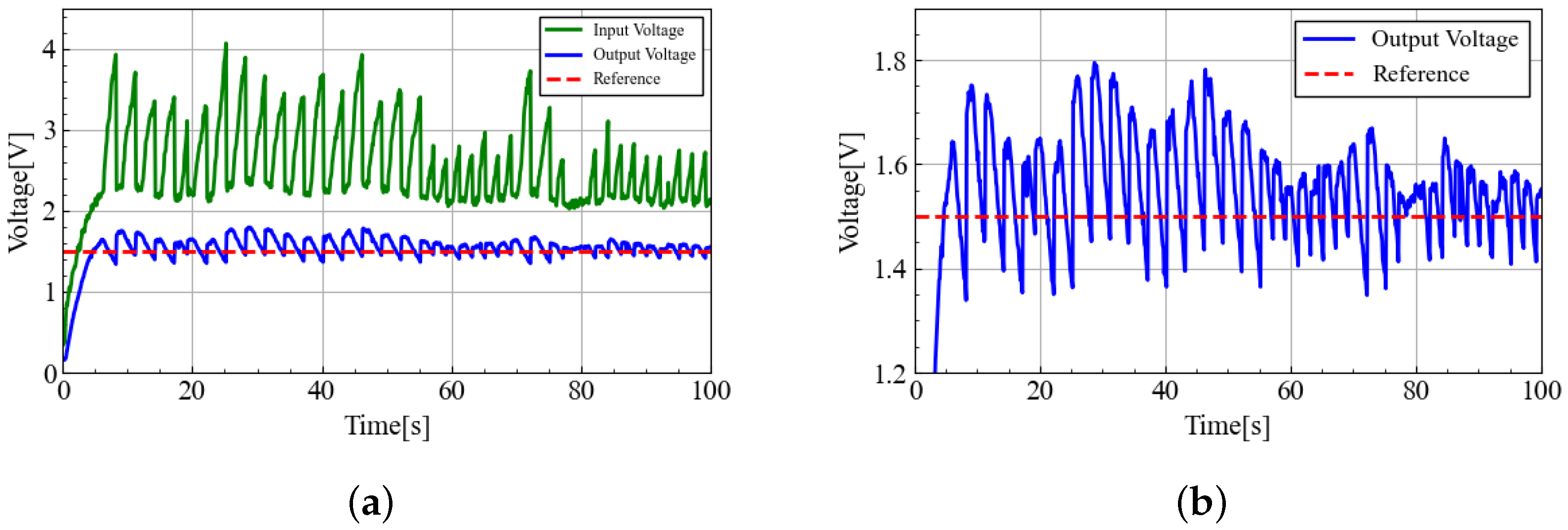
5.1. Simulation Results

In this section, the simulation results of the proposed control system are presented. The simulation primarily focused on the control of a DC–DC converter. Therefore, the input voltage in the simulation was set independently of the TENG’s input voltage. The simulation method involved implementing the control system designed in Section 4 and substituting the control input into the plant model expression for the input u, as described in Equation (10), to observe how the output changes. A numerical analysis was performed using the Runge–Kutta method. The input voltage was configured to change every 10 s as follows: from 2 V to 6 V , from 6 V to 8 V , and from 8 V to 3.5 V . This was carried out to examine whether the output voltage could still track the target value despite rapid fluctuations in the input voltage. The parameters used in the simulation are listed in Table 1. The simulation results of the proposed control system are illustrated in Figure 11. In Figure 11, it can be observed that, despite significant fluctuations in the input voltage, the system follows the reference value. However, it is important to note that the plant model used in the simulation as the control target is the same as the model used in the control system design, and there is no uncertainty involved.

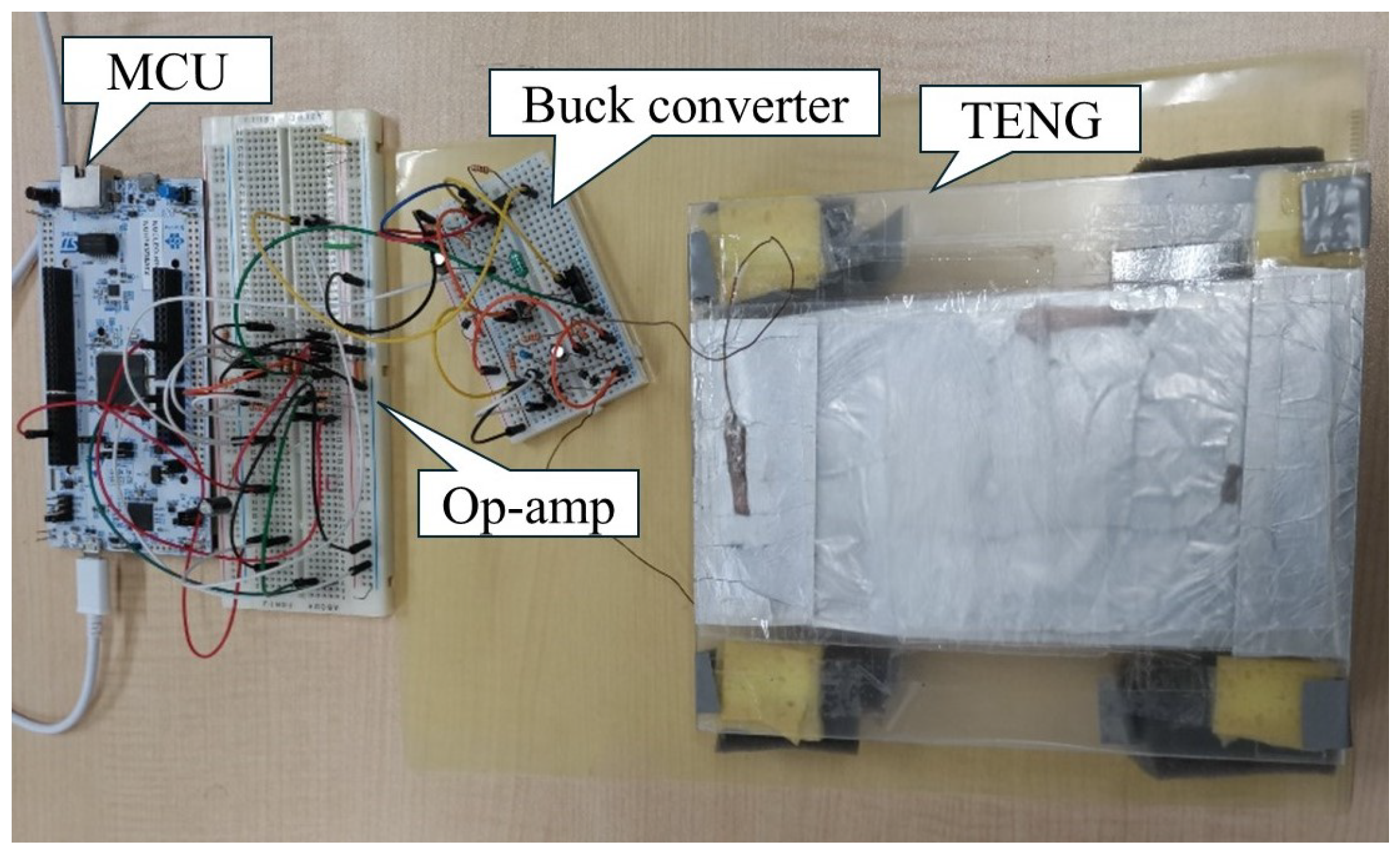
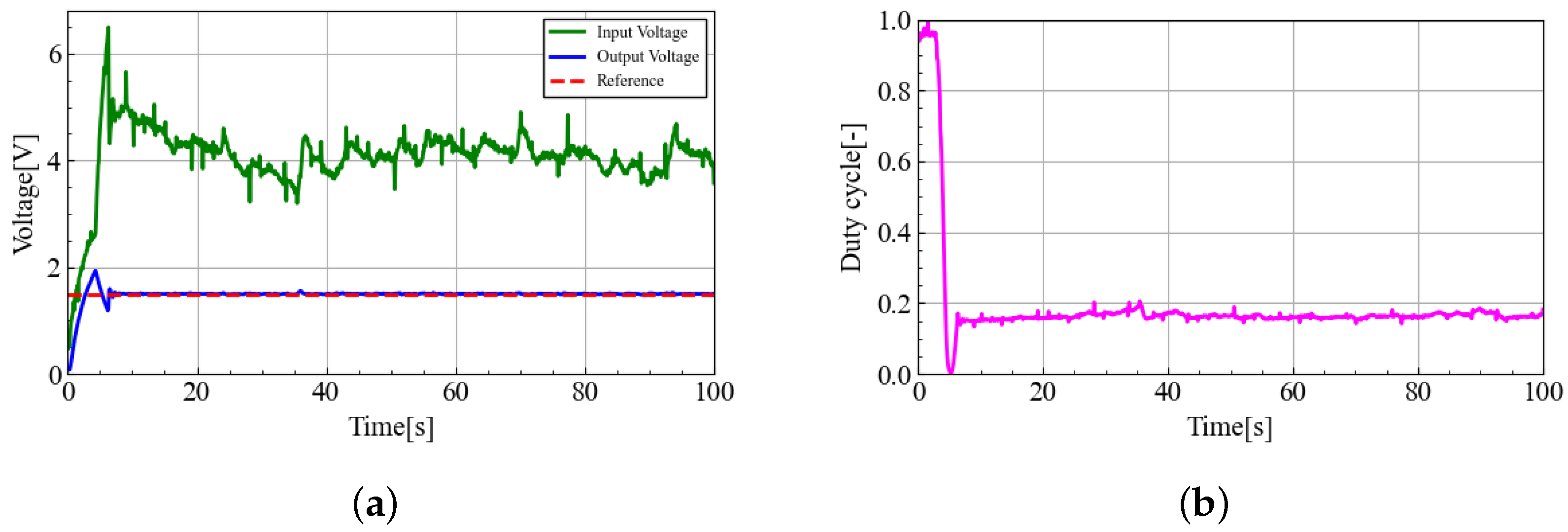
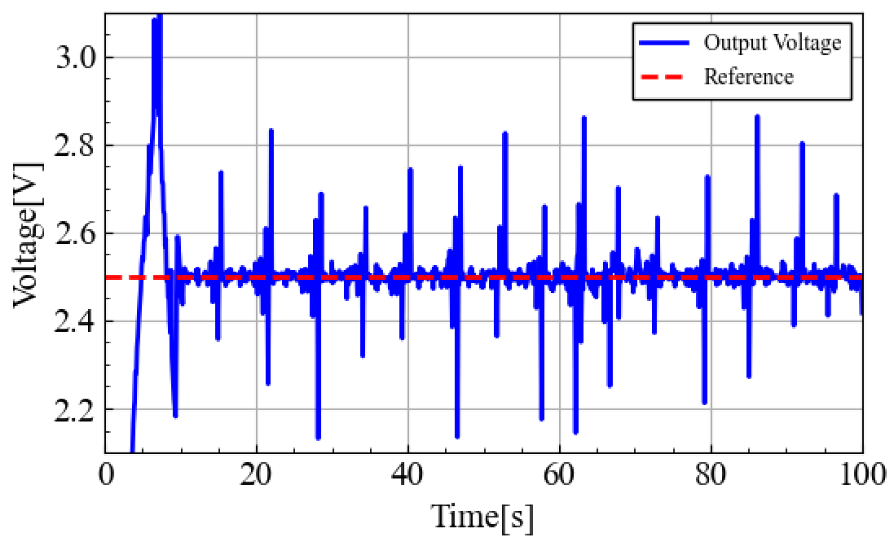
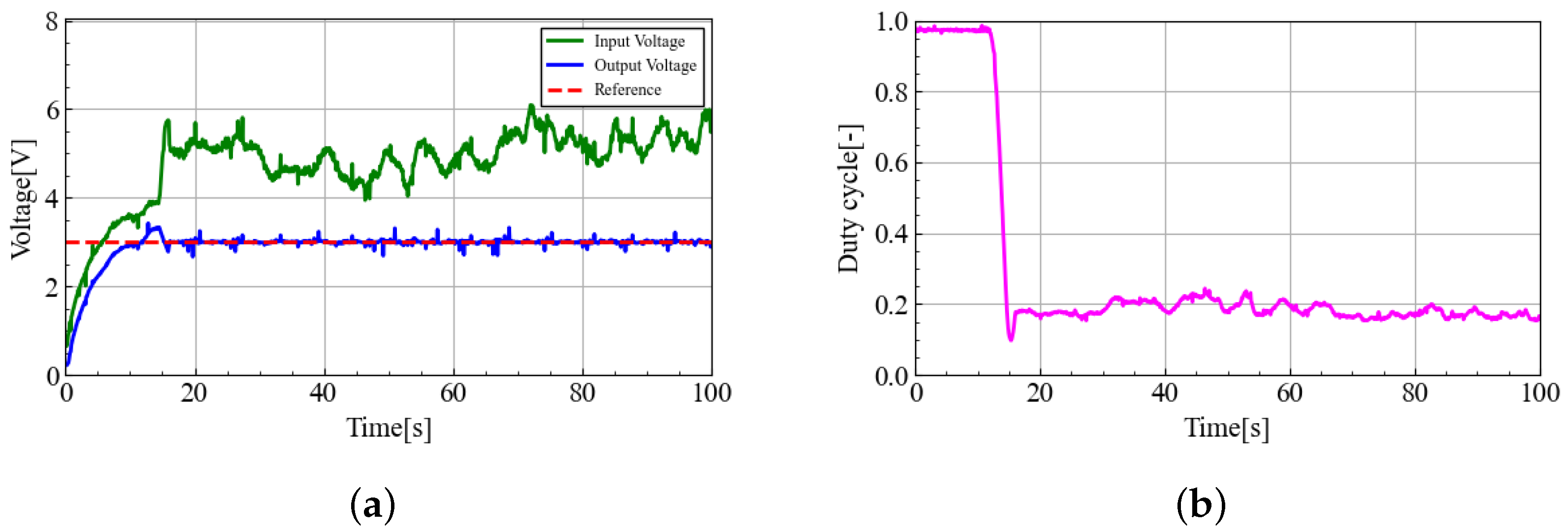
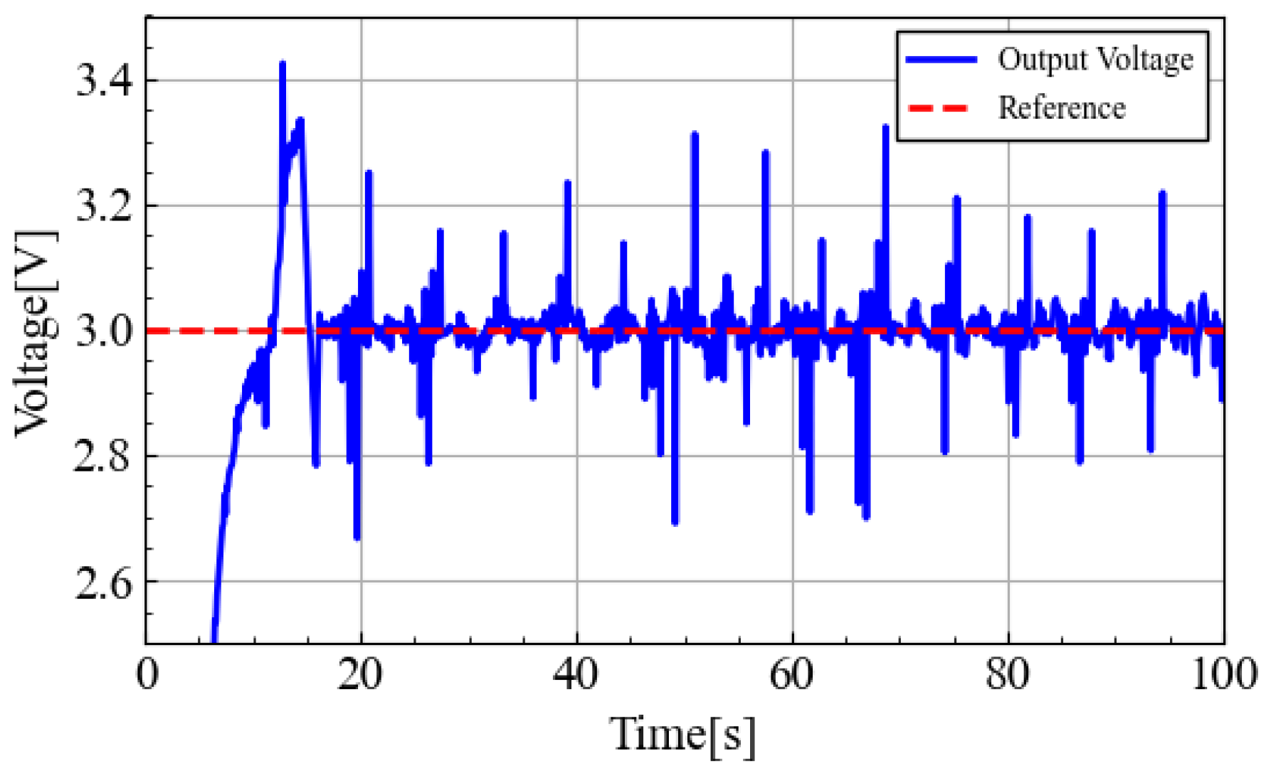
5.2. Experimental Results

This section presents the results obtained from experiments conducted using the actual equipment. An image of the equipment is provided in Figure 12. The experimental setup consists of a TENG, a DC–DC converter, an operational amplifier (op-amp), and a microcontroller (MCU). The op-amp is used for voltage measurement, while the microcontroller performs control calculations. Additionally, the dielectric layer of the TENG is composed of silicon, while the electrode is made of copper plates. This TENG is measured using an oscilloscope with an internal impedance of 10 M Ω , recording a maximum voltage of 265 V . As a result, it generates approximately 0.065 W in instantaneous values; however, this output is only temporary and lacks sustainability.
The parameters used in the experimental setup are presented in Table 2, while the results of the control experiments conducted on the actual device are shown in Figure 13. Although overshoot occurs, it can be confirmed that the output voltage follows the target value under conditions where the input voltage continuously fluctuates. Although the voltage fluctuates more frequently compared to the simulation, it generally follows the target value. However, compared to the simulation, small variations in the output voltage can be observed. It is considered that uncertainties, which were not accounted for during the simulation, may also be one of the causes. The variation in the output voltage after tracking the target value is approximately ± 0.02 V, as shown in Figure 14. The cause of the overshoot is considered as follows: When the difference between the input voltage and the output voltage is small, the duty ratio, which serves as the control input, becomes large. However, as the output voltage follows 1.5 V, the difference between the input and output voltage increases, leading to a rapid decrease in the duty ratio, which results in the occurrence of the overshoot.
Furthermore, experiments were conducted with the target values set to 2.5 V and 3 V. Regarding the parameters, only the load resistance was changed to 4.4 M Ω due to output power considerations.
Although there is some noise, it can be observed that the output voltage generally follows the target value, both when the target is 2.5 V and 3 V. In Figure 15, Figure 16, Figure 17 and Figure 18, it can be observed that there is noise of approximately 0.2 to 0.3 V. As the resistance value increases, the influence of noise becomes more significant. Therefore, a large resistance value can be considered one of the contributing factors. Furthermore, as the resistance value increases, it becomes more difficult for the capacitor to release its charge, which makes the control more challenging. This can also be considered one of the contributing factors.
As a comparison with the proposed control method, experiments were conducted using the commonly used PI control. The experimental setup is identical to the one shown in Figure 12. The parameters are the same as those in Table 2, except for the time constant. Note that the proportional gain is 0.6, and the integral gain is 0.7.
A comparison of Figure 13 and Figure 19 reveals that the proposed method results in smaller fluctuations in the output voltage.

6. Conclusions

This paper presents the development of an output voltage control system for a TENG using a DC–DC converter, with its effectiveness demonstrated through simulations and experiments. The proposed control system is designed based on a model obtained using the WASAM, which also compensates for the nonlinearity of DCM. Furthermore, by performing right coprime factorization combined with a low-pass filter, the system is able to accurately track the target value. Additionally, experiments are conducted using PI control, and the superiority of the proposed method is confirmed. In the future, a control system compatible with pulse-frequency modulation (PFM), where both the duty cycle and switching frequency vary, will be designed. Additionally, a control system that takes overshoot into account will be developed to achieve accurate target value tracking while also considering efficiency.

Author Contributions

Investigation, R.S.; Data curation, C.L.; Formal analysis, C.L.; Methodology, M.D.; Software, R.S.; Supervision, M.D.; Validation, R.S.; Writing—original draft, R.S. All authors have read and agreed to the published version of the manuscript.

Funding

This research received no external funding.

Institutional Review Board Statement

Not applicable.

Informed Consent Statement

Not applicable.

Data Availability Statement

The data presented in this study are available on request from the corresponding author due to privacy considerations.

Conflicts of Interest

The authors declare no conflicts of interest.

References

  1. Wang, Y.; Yang, Y.; Wang, Z.L. Triboelectric Nanogenerators as Flexible Power Sources. NPJ Flex. Electron. 2017, 1, 10. [Google Scholar] [CrossRef]
  2. Yang, Y.; Zhou, Y.S.; Zhang, H.; Liu, Y.; Lee, S.; Wang, Z.L. A Single-Electrode Based Triboelectric Nanogenerator as Self-Powered Tracking System. Adv. Mater. 2013, 25, 6594–6601. [Google Scholar] [CrossRef] [PubMed]
  3. Wang, S.; Lin, L.; Xie, Y.; Jing, Q.; Niu, S.; Wang, Z. Sliding-Triboelectric Nanogenerators Based on In-Plane Charge-Separation Mechanism. Nano Lett. 2013, 13, 2226–2233. [Google Scholar] [CrossRef]
  4. Zhang, H.; Yao, L.; Quan, L.; Zheng, X. Theories for Triboelectric Nanogenerators: A Comprehensive Review. Nanotechnol. Rev. 2020, 9, 610–625. [Google Scholar] [CrossRef]
  5. Cui, X.; Yu, C.; Wang, Z.; Wan, D.; Zhang, H. Triboelectric Nanogenerators for Harvesting Diverse Water Kinetic Energy. Micromachines 2022, 13, 1219. [Google Scholar] [CrossRef]
  6. Liu, Y.; Sun, N.; Liu, J.; Wen, Z.; Sun, X.; Lee, S.T.; Sun, B. Integrating a Silicon Solar Cell with a Triboelectric Nanogenerator via a Mutual Electrode for Harvesting Energy from Sunlight and Raindrops. ACS Nano 2018, 12, 2893–2899. [Google Scholar] [CrossRef]
  7. Ahmed, A.; Hassan, I.; Mosa, M.I.; Elsanadidy, E.; Phadke, S.G.; El-Kady, F.M.; Rusling, F.J.; Selvaganapathy, R.P.; Kaner, B.R. All Printable Snow-Based Triboelectric Nanogenerator. Nano Energy 2019, 60, 17–25. [Google Scholar] [CrossRef]
  8. Luo, J. Recent Progress of Triboelectric Nanogenerators: From Fundamental Theory to Practical Applications. EcoMat 2020, 2, e12059. [Google Scholar] [CrossRef]
  9. Wu, C.; Wang, A.C.; Ding, W.; Guo, H.; Wang, Z.L. Triboelectric Nanogenerator: A Foundation of The Energy for The New Era. Adv. Energy Mater. 2019, 9, 1802906. [Google Scholar] [CrossRef]
  10. Wang, Z.L. Triboelectric Nanogenerators as New Energy Technology for Self-Powered Systems and as Active Mechanical and Chemical Sensors. ACS Nano 2013, 7, 9533–9557. [Google Scholar] [CrossRef]
  11. Kawaguchi, A.; Uchiyama, H.; Matsunaga, M.; Ohno, Y. Simple and Highly Efficient Intermittent Operation Circuit for Triboelectric Nanogenerator Toward Wearable Electronic Applications. Appl. Phys. Express 2021, 14, 057001. [Google Scholar]
  12. Huang, Y.-J.; Chung, C.-K. Research on Performance Enhancement, Output Regulation, and the Applications of Nanogenerators. Micromachines 2025, 16, 208. [Google Scholar] [CrossRef] [PubMed]
  13. Hu, T.; Wang, H.; Harmon, W.; Bamgboje, D.; Wang, L. Current Progress on Power Management Systems for Triboelectric Nanogenerators. IEEE Trans. Power Electron. 2022, 37, 9850–9864. [Google Scholar]
  14. Li, X.; Zhang, C.; Gao, Y.; Zhao, Z.; Hu, Y.; Yang, O.; Liu, L.; Zhou, L.; Wang, J.; Wang, Z.L. A Highly Efficient Constant-Voltage Triboelectric Nanogenerator. Energy Environ. Sci. 2022, 15, 1334–1345. [Google Scholar]
  15. Huang, Y.-J.; Chung, C.-K. Design and Fabrication of Polymer Triboelectric Nanogenerators for Self-Powered Insole Applications. Polymers 2023, 15, 4035. [Google Scholar] [CrossRef]
  16. Endo, H.; Deng, M. Electric Power Control of Thermoelectric Generation System. In Proceedings of the International Conference on Power, Energy and Electrical Engineering, Shiga, Japan, 26–28 February 2021; pp. 215–219. [Google Scholar]
  17. Singh, G.; Kundu, S. An Efficient DC-DC Boost Converter for Thermoelectric Energy Harvesting. AEU-Int. J. Electron. Commun. 2020, 118, 153132. [Google Scholar]
  18. Liu, C.; Shimane, R.; Deng, M. Operator-Based Triboelectric Nanogenerator Power Management and Output Voltage Control. Micromachines 2024, 15, 1114. [Google Scholar] [CrossRef]
  19. Wen, N.; Liu, Z.; Wang, W.; Wang, S. Feedback Linearization Control for Uncertain Nonlinear Systems Via Generative Adversarial Networks. ISA Trans. 2024, 146, 555–566. [Google Scholar]
  20. Yu, X.; Okyay, K. Sliding-Mode Control with Soft Computing: A Survey. IEEE Trans. Ind. Electron. 2009, 56, 3275–3285. [Google Scholar]
  21. Rigatos, G.; Siano, P.; Melkikh, A.; Zervos, N. A Nonlinear H-Infinity Control Approach to Stabilization of Distributed Synchronous Generators. IEEE Syst. J. 2018, 12, 2654–2663. [Google Scholar]
  22. Deng, M.; Inoue, A.; Ishikawa, K. Operator-Based Nonlinear Feedback Control Design Using Robust Right Coprime Factorization. IEEE Trans. Autom. 2006, 51, 645–648. [Google Scholar]
  23. Deng, M.; Saijo, N.; Gomi, H.; Inoue, A. A Robust Real Time Method for Estimating Human Multijoint Arm Viscoelasticity. Int. J. Innov. Comput. Control 2006, 2, 705–721. [Google Scholar]
  24. Zenteno-Torres, J.; Cieslak, J.; Dávila, J.; Henry, D. Sliding Mode Control with Application to Fault-Tolerant Control: Assessment and Open Problems. Automation 2021, 2, 1–30. [Google Scholar] [CrossRef]
  25. Utkin, V.; Lee, H. Chattering Problem in Sliding Mode Control Systems. IFAC Proc. Vol. 2006, 39, 1. [Google Scholar]
  26. Deng, M.; Inoue, A.; Goto, S. Operator Based Thermal Control of an Aluminum Plate with a Peltier Device. Int. J. Innov. Comput. Inf. Control 2008, 4, 3219–3229. [Google Scholar]
  27. Cho, S.; Jang, S.; La, M.; Yun, Y.; Yu, T.; Park, J.S.; Choi, D. Facile Tailoring of Contact Layer Characteristics of the Triboelectric Nanogenerator Based on Portable Imprinting Device. Materials 2020, 13, 872. [Google Scholar] [CrossRef]
  28. Wang, H.; Funaki, H.; Noge, Y.; Shoyama, Y. Widely Applicable Statespace Average Method. Tech. Comm. Energy Eng. Electron. Commun. 2023, 122, 418. (In Japanese) [Google Scholar]
  29. Tanabata, Y.; Deng, M. Filtered Right Coprime Factorization and Its Application to Control a Pneumatic Cylinder. Processes 2024, 12, 1475. [Google Scholar] [CrossRef]
  30. Chen, G.; Han, Z. Robust Right Coprime Factorization and Robust Stabilization of Nonlinear Feedback Control Systems. IEEE Trans. Autom. Control 1998, 43, 1505–1509. [Google Scholar]
Figure 1. Operation mechanism of the TENG and charge transfer.
Applsci 15 04054 g001
Figure 2. The equivalent circuit of the TENG.
Applsci 15 04054 g002
Figure 3. The TENG system with the buck converter.
Applsci 15 04054 g003
Figure 4. The pulse-width modulation (PWM) illustration with ON time ( T O N ) and PWM period (T).
Applsci 15 04054 g004
Figure 5. Equivalent circuits that vary depending on the switch state: (a) equivalent circuit in the ON state, (b) equivalent circuit in the OFF state.
Applsci 15 04054 g005
Figure 6. Variation in inductor current within a PWM cycle: (a) the definitions of the d ^ 1 , d ^ 2 , and d ^ 3 intervals according to the current state, (b) the d ^ 1 , d ^ 2 , and d ^ 3 intervals expressed in a PWM period.
Applsci 15 04054 g006
Figure 7. Equivalent circuit when the inductor current is zero.
Applsci 15 04054 g007
Figure 8. Conceptual diagram of right factorization.
Applsci 15 04054 g008
Figure 9. Conceptual diagram of filtered right factorization.
Applsci 15 04054 g009
Figure 10. Control system based on operator theory.
Applsci 15 04054 g010
Figure 11. Simulation results of output voltage control: (a) output voltage of the buck converter, (b) control input (duty cycle).
Applsci 15 04054 g011
Figure 12. The buck converter connected to the TENG and its circuit for measurement and control.
Applsci 15 04054 g012
Figure 13. Experimental results of output voltage control: (a) output voltage of the buck converter connected to the TENG, (b) control input (duty cycle).
Applsci 15 04054 g013
Figure 14. Enlarged view of the output voltage.
Applsci 15 04054 g014
Figure 15. Experimental results of output voltage control with a target value of 2.5 V: (a) output voltage of the buck converter connected to the TENG, (b) control input (duty cycle).
Applsci 15 04054 g015
Figure 16. Enlarged view of the output voltage when the target value is 2.5 V.
Applsci 15 04054 g016
Figure 17. Experimental results of output voltage control with a target value of 3 V: (a) output voltage of the buck converter connected to the TENG, (b) control input (duty cycle).
Applsci 15 04054 g017
Figure 18. Enlarged view of the output voltage when the target value is 3 V.
Applsci 15 04054 g018
Figure 19. Experimental results of PI control: (a) output voltage of the buck converter connected to the TENG, (b) enlarged view of the output voltage with the PI control.
Applsci 15 04054 g019
Table 1. Simulation parameters.
ParameterDefinitionValue
fSampling Frequency 4 KHz
V r e f Reference Voltage 1.5 V
R l o a d Load Resistance 2.2 M Ω
LInductance 0.01 H
C o u t Output Capacitor 2.2 μ F
f S W Switching Frequency 1 KHz
τ Time Constant 0.005 ms
Table 2. Experimental parameters.
ParameterDefinitionValue
fSampling Frequency 4 KHz
d 0 The Thickness of the Dielectric 1 mm
V r e f Reference Voltage 1.5 V
R l o a d Load Resistance 2.2 M Ω
LInductance 0.01 H
C i n Input Capacitor 0.47 μ F
C o u t Output Capacitor 2.2 μ F
f S W Switching Frequency 1 KHz
x m Maximum Distance Between the Layers25 mm
SElectrode’s Area 0.01 m 2
T b Vibration Period 0.4 s
τ Time Constant 5 ms
Disclaimer/Publisher’s Note: The statements, opinions and data contained in all publications are solely those of the individual author(s) and contributor(s) and not of MDPI and/or the editor(s). MDPI and/or the editor(s) disclaim responsibility for any injury to people or property resulting from any ideas, methods, instructions or products referred to in the content.

