Abstract
In this paper, a novel multiple-input operational transconductance amplifier (MI-OTA) is proposed. The MI-OTA can be obtained by using the multiple-input bulk-driven MOS transistor (MIBD MOST) technique. The circuit structure is simple, can operate with a supply voltage of 0.5 V, and consumes 937 pW at a current setting of 625 pA. The proposed MI-OTA was used to implement a high-order multiple-input voltage-mode universal filter. The proposed filter can provide non-inverting and inverting low-pass, high-pass, band-pass, band-stop, and all-pass transfer functions to the same topology. In addition, it has a high input impedance and does not need any inverted input signals, so there is no additional buffering circuit. The proposed filter can be used for biological signal processing. The proposed MI-OTA and the second-order universal filter were simulated in Cadence using CMOS process parameters of 0.18 μm from TSMC to verify the functionality and performance of the new structures.
1. Introduction
Analog filters can be used as the front end of biomedical systems to select the frequency range, to eliminate out-of-band noise, and to suppress 50/60 Hz power line interference in biological signals before further processing by a digital signal processor. A typical block diagram of a biomedical system is shown in Figure 1 as an example, where the inputs to this system are biosignals such as electroencephalographic (EEG), electromyographic (EMG), and electrocardiographic (ECG) signals from biosensors. These input signals may contain interfering noise, and their amplitude and frequency range are low, i.e., amplitude 15 µV–5 mV, frequency range 0.05–250 Hz [1]. To be more precise, the frequency/amplitude ranges of EEG, EMG, and ECG signals are 0.05–60 Hz/15–100 µV, 10–200 Hz/0.1–5 mV, and 0.05–250 Hz/100 µV–5 mV, respectively.
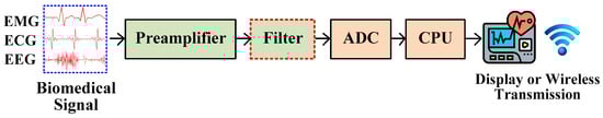
Figure 1.
Block diagram of a typical biomedical signal processing.
In Figure 1, the preamplifier amplifies the low-amplitude signal, while the analog filter selects the frequency range and removes out-of-band noise. The filtered analog signal is converted to digital form by an analog-to-digital converter (ADC) and then further processed by a central processing unit (CPU) block. In an analog filter, a low-pass filter is typically used to select the frequency range and remove out-of-band noise [2]. A band-pass filter is typically used to select the desired frequency band and reduce out-of-band noise [3]. A notch/low-pass notch filter is typically used to suppress 50/60 Hz power line interference [4]. In addition, an all-pass filter can be used in hearing aids [5]. Thus, universal filters can be used in biomedical systems, which can realize low-pass filters (LPF), band-pass filters (BPF), band-stop filters (BSF), and all-pass filters (APF).
Many active filters are available in the open literature for various applications in biomedical systems [3,6,7,8,9,10,11,12,13,14,15,16,17,18,19]. First-order filters are presented in [6,7,8], second-order filters in [9,10,11,12,13], and third-order filters in [14,15,16]. Fourth-order filters are presented in [3,17], and fifth-order filters are presented in [19,20,21,22]. Sixth-order filters are presented in [23,24,25,26], and ninth-order filters are presented in [27]. In other words, different biomedical applications require filters of different orders depending on the specific bio-signal characteristics and the type of noise or artifacts present.
Many versatile high-order filters based on various active devices are available in the literature [28,29,30,31,32,33,34,35,36,37,38,39,40]. The filters in [28,29,30,31,32] use current conveyors, while the filter in [33] uses current feedback operational amplifiers (CFOA). However, filters based on these active elements lack electronic tuning capability and require many passive resistors. Filters using current-controlled current conveyors in [34], operational transconductance amplifiers (OTA) [35,36,37,38,39,40] provide electronic tuning capability that can easily compensate for natural frequency when it is affected by process and temperature variations. The high-order structures in [37,38,39,40] consume low power and provide variant filtering functions, i.e., LPF, HPF, and BPF.
In this paper, a high-order universal filter using multiple-input operational transconductance amplifiers (MI-OTA) is proposed. The multiple-input OTA can be realized by using the multiple-input bulk-driven MOS transistor (MIBD-MOST) technique. The MI-OTA can operate with a supply voltage of 0.5 V and consumes very low power by employing MOST operating in the subthreshold region. The MIBD-MOST technique simplifies the CMOS structure of the OTA by using only one differential pair, thus avoiding the increase in current branches that would otherwise lead to higher power consumption. Additionally, the multiple inputs of the OTA enable support for the proposed high-order universal filter, which provides various filtering functions with both non-inverting and inverting voltage transfer functions within a single topology. For instance, first-, second-, and third-order universal filters are presented, which can be derived from the proposed nth-order universal filter. The proposed MI-OTA and the selected second-order universal filter are designed and simulated on the Cadence platform using 0.18 µm CMOS technology from TSMC.
The research paper is organized as follows: Section 2 presents a description of the circuit, which includes the proposed MI-OTA and the proposed nth-order universal filter. In this section, the first, second, and third-order universal filters are also presented from the proposed nth-order universal filter. In Section 3, the design of the proposed MI-OTA and the second-order universal filter on the Cadence platform is verified, and the performance of the proposed filter is compared with some previous works. Finally, Section 4 concludes the paper.
2. Proposed Circuit
2.1. MI-OTA
The circuit symbol of the MI-OTA is shown in Figure 2. The OTA has two inverting and two non-inverting inputs. In an ideal case, its voltage-to-current transfer characteristic is described by the following equation:
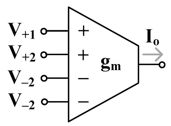
Figure 2.
Symbol of MI-OTA.
Here, represents the output current , are the non-inverting input voltages , are the inverting input voltages, and denotes the transconductance gain. Thus, the output current is proportional to the difference of two sums of signals applied to the non-inverting and inverting inputs, respectively, where is the circuit transconductance.
The simple CMOS realization of the MI-OTA proposed in this work is shown in Figure 3. The circuit is composed of two BD non-symmetrical differential pairs (M1–M2 and M3–M4), biased by the current sources M5 and M6 and loaded by the current mirror M7–M8, composed of self-cascode (SC) transistors for larger output resistance and DC voltage gain. The non-symmetrical differential pairs allow increasing the linear range of the OTA. The linearization principle was adopted from [41], where a bipolar and generalized (multiple-pair) version of this circuit was described. In [42], a GD CMOS version of the circuit was presented. Using the formula provided in [42] and replacing the input differential voltage at the gates by the input differential voltage at the bulks, the DC transfer characteristic of OTA, operating in weak inversion, can be expressed as:
where is the differential voltage between bulk terminals of M1 and M3, is the subthreshold slope factor for a p-channel MOS, is the bulk-to-gate transconductance ratio at the operating point, is the thermal potential and = (W/L)1/(W/L)2 = (W/L)3/(W/L)4 is the ratio of aspect ratios of M1 and M2 (M3 and M4).
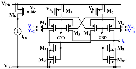
Figure 3.
CMOS implementation of MI-OTA.
The linear range of OTA depends on coefficient m. By equaling the second derivative of (2) to zero, the optimal linearity is achieved for = or =. This result is independent of the biasing currents and . In the optimal case, the linear range of this transconductor, determined for 1% variation , is nearly four times larger than the one for the classic BD differential pair operating in weak inversion.
In the proposed MI structure, a BD-MI technique, which was first experimentally verified in [43,44], has been applied to increase the number of its inputs. The BD transistors M1 and M3 have been replaced by BD-MI composite transistors. Their symbol and circuit implementation are shown in Figure 4a and Figure 4b, respectively. The MIs were realized using a capacitive divider/voltage summing circuit composed of capacitors . In order to properly bias the bulk terminals of M1–M4 for DC, the capacitors are shunted by large resistances , realized as an anti-parallel connection of MOS transistors operating in the cut-off region with , as shown in Figure 4c. This approach allows avoiding the use of additional transistors (input stages); namely, it simplifies the structure and allows saving power. Moreover, the voltage attenuation introduced by the input capacitive divider further expands the linear range of the OTA.
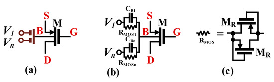
Figure 4.
MI-MOS transistor: (a) symbol, (b) realization, (c) realization of RMOS.
For frequencies above and identical capacitances , the AC voltage at the bulk terminal of M1 (M3) can be expressed as:
where is the AC voltage gain of the input capacitive divider from the i-th input equal to:
Assuming identical capacitances , which entails and ID5 = ID6 = Iset, the quasi-static transfer characteristic of OTA from the i-th differential input, with the other differential input shorted to ground, can be expressed as:
From (5), the small-signal transconductance of the OTA, around can be calculated as:
For the optimal case (= 3.732), the above expression simplifies to:
where for a 2-input OTA with identical capacitances is equal to 1/2.
As it can be concluded from (7), the circuit transconductance is proportional to the biasing current and can be easily regulated using this current.
The OTA could be realized using a current mirror topology; however, to simplify the overall structure, a simpler architecture of a single differential stage has been chosen. Its output voltage without load is equal to ; therefore, to maintain its value equal to zero, should be equal to at the operating point. On the other hand, the voltages for M1–M4 were chosen to be equal to about , which allows operating M5 and M6 in saturation, also with possible () adjustments and PVT changes.
As mentioned previously, transistors M7 and M8 are realized as composite SC devices, which allows increasing their output resistance without limiting output swing. Only n-channel transistors were realized in this way, because for p-channel transistors this could affect linearity. Moreover, output conductances of n-channel devices are larger; therefore, their impact on the output resistance of OTA and consequently its voltage gain is more significant.
The low-frequency voltage gain of OTA, from one differential input, is given by:
The input referred noise of the OTA can be expressed as:
where is the mean-square output noise current, which, assuming perfect symmetry and neglecting second-order effects, can be expressed as:
Note that due to the non-symmetry of input pairs, transistors M5 and M6 contribute to the overall noise. The noise current of an MOS device consists of thermal and components and, in weak inversion is given by:
where is the electron charge, is the quiescent drain current of the i-th device, is its transconductance, is the oxide capacitance per unit area, is the flicker noise constant, and W and L are the channel width and length, respectively.
In LV and LP designs, due to low biasing currents and relatively large transistor sizes, usually the thermal noise component is dominant in the frequency range of interest. Taking into account only the thermal noise component, the output noise current can be expressed as:
From (7), (9), and (12), the input referred noise is
Thus, the input referred noise is increased by the signal attenuation introduced by the input capacitive divider (β) and BD technique (η). However, since the linear range is increased in the same proportion, the dynamic range of OTA is the same as for a single-input gate-driven version of the circuit.
2.2. Proposed High-Order Universal Filter
The proposed nth-order universal filter using MI-OTA is shown in Figure 5. It uses n + 1 MI-OTAs and n grounded capacitors. Note that the input terminals of the universal filter are connected to the high-impedance terminals of the OTA; hence, the filter has a high input impedance. Signals can therefore be applied to the filter inputs without the requirement for buffer circuits. The universal filter using multiple-input OTAs (including plus/minus terminals) can easily provide the non-inverting and inverting transfer functions of a low-pass filter (LPF), high-pass filter (HPF), band-pass filter (BPF), band-stop filter (BSF), and all-pass filter (APF) without the additional requirements of an inverting input amplifier. The use of a grounded capacitor facilitates compensation for parasitic circuit capacitances.
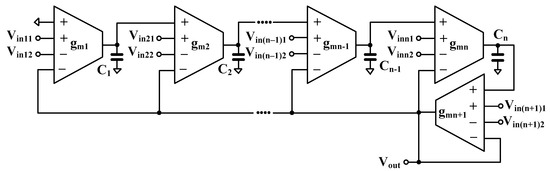
Figure 5.
Proposed nth-order universal filter using MI-OTAs.
To represent the operation of the system in Figure 5, the first-, second-, and third-order universal filters have been designed as an example. Figure 6 shows the first-order universal filter that employs two OTAs and one grounded capacitor. The output voltage can be expressed by
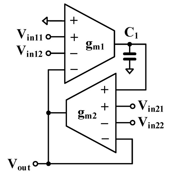
Figure 6.
First-order universal filter.
The pole frequency of the filter can be given by
With the first-order universal filter using MI-OTA, variant filter functions LPF, HPF, and APF can be obtained under suitable conditions as shown in Table 1. Inputs to which no input signal is applied should be connected to ground to prevent noise injection.

Table 1.
Obtaining variant filtering functions of the first-order universal filter.
The second-order universal filter that employs three OTAs and two grounded capacitors is shown in Figure 7. The output voltage can be expressed by
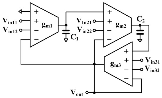
Figure 7.
Second-order universal filter.
Variants of the filter functions LPF, HPF, BPF, BSP, and APF can be obtained by appropriate use of the input signals as shown in Table 2.
Table 2.
Obtaining variant filtering functions of the second-order universal filter.
The natural frequency () and the quality factor () can be given respectively by
The third-order universal filter that employs four OTAs and three grounded capacitors is shown in Figure 8. The output voltage can be expressed by
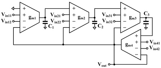
Figure 8.
Third-order universal filter based on n-order filter.
Variants of the LPF, HPF, BPF, and APF filter functions can be obtained by appropriate use of the input signals as shown in Table 3.
Table 3.
Obtaining variant filtering functions of the third-order universal filter.
Letting the parameters and of filters be given, respectively, by
3. Simulation Results
The MI-OTA circuit and filter applications were designed and simulated in Cadence using 0.18 µm CMOS technology from TSMC. The supply voltage was 0.5 V (±0.25 V). The transistor aspect ratios in Figure 2 are listed in Table 4. Note that the ratio of the aspect ratios for M1,3 and M2,4 meets the requirement . The power consumption of the MI-OTA at = 625 pA was 937 pW.
Table 4.
Component values of the proposed MI-OTA.
Figure 9 shows the DC characteristics of the output current and small-signal transconductance of the OTA with and without MI for = 625 pA when the output terminal is grounded. As can be seen, the linearity and input voltage range are expanding thanks to the MI technique.
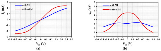
Figure 9.
DC transfer characteristics of the OTA with and without MI for = 625 pA; (a) output currents , and (b) small-signal transconductance .
Figure 10 shows the frequency characteristic of the MI-OTA output impedance for = 625 pA with and without SC. While shows 2.56 GΩ for the structure without SC, it shows 4.08 GΩ for the structure with SC, so the improvement in impedance is obvious.
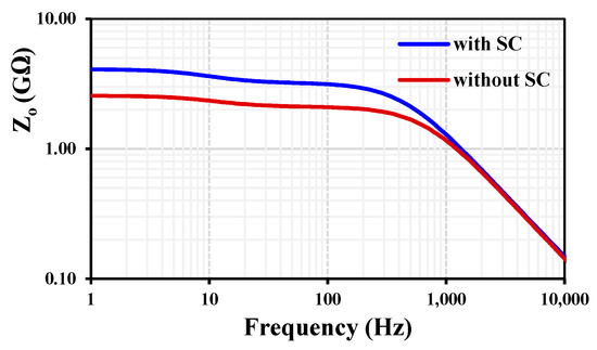
Figure 10.
Frequency characteristic of the output impedance of the MI-OTA for = 625 pA with and without SC.
The transient response of the MI-OTA with applied input sine wave = 250 mV@1 kHz for = 625 pA is shown in Figure 11. The total harmonic distortion (THD) was around 1.2%.
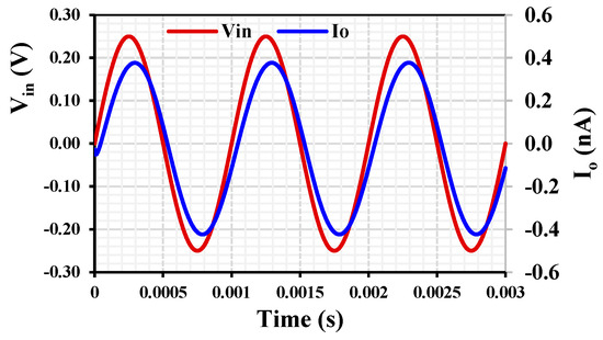
Figure 11.
Transient response of the MI-OTA with 250 mV input amplitudes and 1 kHz frequency.
Figure 12 shows the DC characteristics of the output current and transconductance characteristics of the MI-OTA for different values of = (0.625, 1.25, 2.5, 5) nA, where wide tunability is achieved.
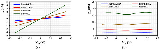
Figure 12.
DC characteristics of the MI-OTA for different ; (a) output currents and (b) small-signal transconductance .
For the filter application, the value of capacitors C1 = C2 = 25 pF was selected for the second-order universal filter. The frequency responses of the LP, HP, BP, BS, and AP gains and phases with setting current = 625 pA with 4 pF load capacitance are shown in Figure 13. The cutoff frequency was 11 Hz while the power consumption was 2.8 nW. Obviously, the filter can reach very low cutoff frequencies, making it suitable for biomedical signal processing.
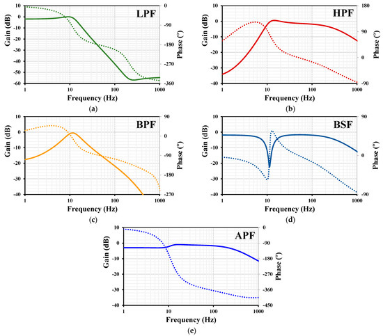
Figure 13.
Frequency characteristics of gains (lines) and phases (dots) with = 625 pA for the LPF (a), HPF (b), BPF (c), BSF (d), and APF (e).
The frequency characteristics of gains (lines) and phases (dots) with different for the: LPF (a), HPF (b), BPF (c), BSF (d), and APF (e) are shown in Figure 14. The wide tunability of the filter was achieved by varying the setting current = (0.625, 1.25, 2.5, 5) nA. The cutoff frequency was (11, 21, 39.8, 75) Hz, respectively.
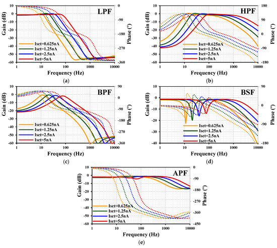
Figure 14.
Frequency characteristics of gains (lines) and phases (dots) with different for the LPF (a), HPF (b), BPF (c), BSF (d), and APF (e).
Figure 15 shows the results of the process and mismatch Monte Carlo (MC) analysis with 200 runs and the process, voltage, and temperature (PVT) corners of the second-order LPF. As can be seen, the curves almost overlap for the MC, process, and power supply voltage corners, with small deviations in the case of the temperature corners due to the sensitivity of the circuit operating in the subthreshold region to temperature changes.
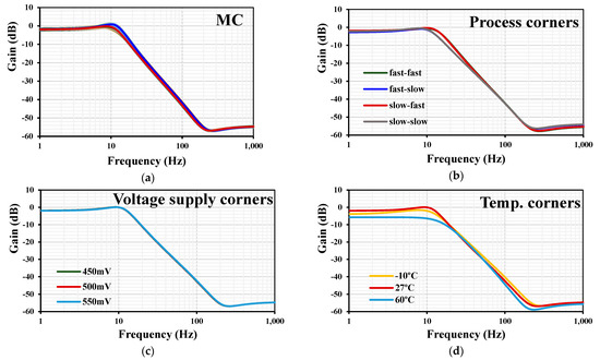
Figure 15.
Frequency characteristics of gains with = 625 pA for the LPF: 200 runs MC (a), process corners (b), voltage supply corners (c), and temperature corners (d).
Figure 16 shows the equivalent output noise of the second-order LPF with = 625 pA. The integrated output noise from 0.01 to 11 Hz was calculated to be 67 µV.
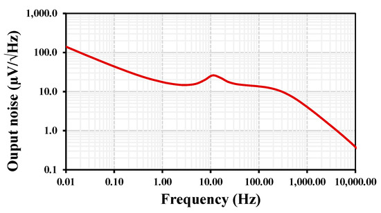
Figure 16.
Output noise of the second-order LPF.
The transient responses of the second-order LPF with applied input sine wave = (25, 50, 100) mV@10 Hz for = 5 nA are shown in Figure 17. The total harmonic distortion (THD) was below 2%.
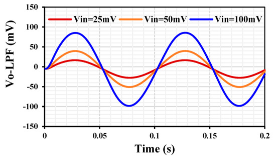
Figure 17.
The transient response of the second-order LPF with different amplitudes of input signal at 10 Hz.
To test the biomedical signal processing filter, a noisy ECG signal, containing 2 mV@400 Hz noise, was applied to the LPF input with = 5 nA. Figure 18 shows the transient characteristics of the noisy ECG used and the signal at the output of the filter where the noise is filtered out.
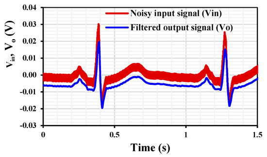
Figure 18.
Transient response of the second-order LPF when a noisy ECG signal is applied to its input and a filtered signal that appears at its output.
Table 5 summarizes a comparison of this work with recently published similar circuits. The second-order LPF for ECG signal processing in [12], the second-order universal filter with ultra-low power consumption for biological signal processing in [13], the nth-order universal filter in [32], and the high-order universal filter with ultra-low power consumption in [38] were selected for comparison. As can be seen from Table 5, the proposed filter has the capability to generate ten filter responses, namely non-inverting and inverting LPF, HPF, BPF, BSP, and APF, without the requirement of an inverted input signal. Compared to [32], the proposed filter has the capability of electronic tuning of natural frequency and has a much lower voltage supply. Compared to [12,13], the proposed filter offers higher DR with lower power consumption. Finally, the proposed filter confirms its suitability for processing biological signals of extremely low frequencies (in the Hertz region).
Table 5.
Comparison of this work with recently published ones.
4. Conclusions
This paper presents a novel low-voltage, ultra-low-power, multiple-input operational transconductance amplifier based on a bulk-driven MOS transistor with a multiple-input technique. In order to express the advantage of the multiple-input OTA, it was used to realize a high-order multiple-input voltage-mode universal filter. It is worth pointing out that the non-inverting and inverting transfer functions of the variant responses of the low-pass, high-pass, band-pass, band-stop, and all-pass filters can be obtained from the same configuration with appropriate arrangement of the input signals. These filter functions were achieved without additional buffering circuits and any inverted input signals because the filter has multiple plus/minus inputs and high input impedance. The natural frequency can be controlled electronically. The proposed MI-OTA and high-order universal filter were designed and verified using a 0.18 µm CMOS process. The MI-OTA can operate with a supply voltage of 0.5 V and consumes 937 pW of power at a current setting of 625 pA. The simulation results of the second-order universal filter confirmed its suitability for processing biological signals of extremely low frequencies.
Author Contributions
Conceptualization, F.K., M.K. and T.K.; methodology, F.K., M.K. and T.K.; software, F.K. and M.K.; validation, F.K., M.K. and S.L.; formal analysis, T.K. and M.K.; investigation, F.K., M.K. and T.K.; resources, M.K.; data curation, F.K. and M.K.; writing—original draft preparation, F.K., M.K., T.K. and S.L.; writing—review and editing, F.K., M.K., T.K. and S.L.; visualization, F.K. and M.K.; supervision, F.K. and M.K.; project administration, F.K. and M.K.; funding acquisition, M.K. All authors have read and agreed to the published version of the manuscript.
Funding
This work was supported in part by the University of Defence within the Organization Development Project VAROPS.
Institutional Review Board Statement
Not applicable.
Informed Consent Statement
Not applicable.
Data Availability Statement
The original contributions presented in this study are included in the article. Further inquiries can be directed to the corresponding author.
Conflicts of Interest
The authors declare no conflicts of interest.
References
- Webster, J.G. Medical Instrumentation: Application and Design, 4th ed.; John Wiley & Sons: Hoboken, NJ, USA, 2010; pp. 11–12. [Google Scholar]
- Lee, S.-Y.; Cheng, C.-J. Systematic Design and Modeling of a OTA-C Filter for Portable ECG Detection. IEEE Trans. Biomed. Circuits Syst. 2009, 3, 53–64. [Google Scholar] [CrossRef] [PubMed]
- Yang, M.; Liu, J.; Xiao, Y.; Liao, H. 14.4 nW Fourth-Order Bandpass Filter for Biomedical Applications. Electron. Lett. 2010, 46, 973–974. [Google Scholar] [CrossRef]
- Thomas, C.W.; Huebner, W.P.; Leigh, R.J. A Low-Pass Notch Filter for Bioelectric Signals. IEEE Trans. Biomed. Eng. 1988, 35, 496–498. [Google Scholar] [CrossRef] [PubMed]
- van Dijk, L.P.L.; van der Woerd, A.C.; Mulder, J.; van Roermund, A.H.M. An ultra-low-power, low-voltage electronic audio delay line for use in hearing aids. IEEE J. Solid-State Circuits 1998, 33, 291–294. [Google Scholar] [CrossRef]
- Wang, R.; Jin, C.; McEwan, A.; van Schaik, A. A programmable axonal propagation delay circuit for time-delay spiking neural networks. In Proceedings of the 2011 IEEE International Symposium of Circuits and Systems (ISCAS), Rio de Janeiro, Brazil, 15–18 May 2011; pp. 869–872. [Google Scholar] [CrossRef]
- Rodriguez-Villegas, E.; Casson, A.J.; Corbishley, P. A Subhertz Nanopower Low-Pass Filter. IEEE Trans. Circuits Syst. II Express Briefs 2011, 58, 351–355. [Google Scholar] [CrossRef]
- Paul, A.; Ramírez-Angulo, J.; Lopez-Martin, A.J.; Carvajal, R.G. CMOS First-Order All-Pass Filter With 2-Hz Pole Frequency. IEEE Trans. Very Large Scale Integr. (VLSI) Syst. 2019, 27, 294–303. [Google Scholar] [CrossRef]
- Martincorena-Arraiza, M.; De La Cruz-Blas, C.A.; Lopez-Martin, A.; Carlosena, A. Micropower Class AB Low-Pass Analog Filter Based on the Super-Source Follower. IEEE Trans. Circuits Syst. II Express Briefs 2022, 69, 3684–3688. [Google Scholar] [CrossRef]
- Carrillo, J.M.; de la Cruz-Blas, C.A. 0.6-V 1.65-μW Second-Order Gm-C Bandpass Filter for Multi-Frequency Bioimpedance Analysis Based on a Bootstrapped Bulk-Driven Voltage Buffer. J. Low Power Electron. Appl. 2022, 12, 62. [Google Scholar] [CrossRef]
- Corbacho, I.; Carrillo, J.M.; Ausín, J.L.; Domínguez, M.A.; Pérez-Aloe, R.; Duque-Carrillo, J.F. CMOS Widely Tunable Second-Order Gm-C Bandpass Filter for Multi-Sine Bioimpedance Analysis. Electronics 2023, 12, 1326. [Google Scholar] [CrossRef]
- Yin, Y.; Zhang, X.; Feng, Z.; Qi, H.; Lu, H.; He, J.; Jin, C.; Luo, Y. An Ultra-Low-Voltage Transconductance Stable and Enhanced OTA for ECG Signal Processing. Micromachines 2024, 15, 1108. [Google Scholar] [CrossRef]
- Namdari, A.; Aiello, O.; Caviglia, D.D. A 0.5 V, 32 nW Compact Inverter-Based All-Filtering Response Modes Gm-C Filter for Bio-Signal Processing. J. Low Power Electron. Appl. 2024, 14, 40. [Google Scholar] [CrossRef]
- Deo, A.; Pandey, S.K.; Joshi, A.; Sharma, S.K.; Shrimali, H. Design of a Third Order Butterworth Gm-C Filter for EEG Signal Detection Application. In Proceedings of the 2018 25th International Conference “Mixed Design of Integrated Circuits and System” (MIXDES), Gdynia, Poland, 21–23 June 2018; pp. 361–365. [Google Scholar] [CrossRef]
- Diab, M.S.; Mahmoud, S.A. Balanced OTA-C Elliptic Cauer Filters for Biomedical Applications. In Proceedings of the 2018 41st International Conference on Telecommunications and Signal Processing (TSP), Athens, Greece, 4–6 July 2018; pp. 1–5. [Google Scholar] [CrossRef]
- Fujii, T.; Matsumoto, F.; Shouno, K. Very Low Frequency Lowpass Filter with Finite Transmission Zeros Realized by Using Extended Symmetrical Impedance Scaling Circuit. In Proceedings of the 2019 34th International Technical Conference on Circuits/Systems, Computers and Communications (ITC-CSCC), JeJu, Republic of Korea, 23–26 June 2019; pp. 1–4. [Google Scholar] [CrossRef]
- Rajan, V.S.; Venkataramani, B. Design of Low Power, Programmable Low-Gm OTAs and Gm-C Filters for Biomedical Applications. Analog Integr. Circuits Signal Process. 2021, 107, 389–409. [Google Scholar] [CrossRef]
- Krishna, M.; Laxminidhi, T. Widely Tunable Lowpass gm-C Filter for Biomedical Applications. IET Circuits Devices Syst. 2019, 13, 239–244. [Google Scholar] [CrossRef]
- Alhammadi, A.A.; Mahmoud, S.A. Fully differential fifth-order dual-notch power line interference filter oriented to EEG detection system with low pass feature. Microelectron. J. 2016, 56, 122–133. [Google Scholar] [CrossRef]
- Sun, C.-Y.; Lee, S.-Y. A Fifth-Order Butterworth OTA-C LPF with Multiple-Output Differential-Input OTA for ECG Applications. IEEE Trans. Circuits Syst. II Express Briefs 2018, 65, 421–425. [Google Scholar] [CrossRef]
- Lee, S.-Y.; Wang, C.-P.; Chu, Y.-S. Low-Voltage OTA-C Filter with an Area- and Power-Efficient OTA for Biosignal Sensor Applications. IEEE Trans. Biomed. Circuits Syst. 2019, 13, 56–67. [Google Scholar] [CrossRef]
- Pinto, P.M.; Ferreira, L.H.C.; Colletta, G.D.; Braga, R.A.A. A 0.25-V fifth-order Butterworth low-pass filter based on fully differential difference transconductance amplifier architecture. Microelectron. J. 2019, 92, 104606. [Google Scholar] [CrossRef]
- Castello, R.; Grassi, A.G.; Donati, S. A 500-nA sixth-order bandpass SC filter. IEEE J. Solid-State Circuits 1990, 25, 669–676. [Google Scholar] [CrossRef]
- Solis-Bustos, S.; Silva-Martinez, J.; Maloberti, F.; Sanchez-Sinencio, E. A 60-dB dynamic-range CMOS sixth-order 2.4-Hz low-pass filter for medical applications. IEEE Trans. Circuits Syst. II Analog Digit. Signal Process. 2000, 47, 1391–1398. [Google Scholar] [CrossRef]
- Corbishley, P.; Rodriguez-Villegas, E. A Nanopower Bandpass Filter for Detection of an Acoustic Signal in a Wearable Breathing Detector. IEEE Trans. Biomed. Circuits Syst. 2007, 1, 163–171. [Google Scholar] [CrossRef]
- Bertsias, P.; Psychalinos, C. Ultra-Low Voltage Sixth-Order Low Pass Filter for Sensing the T-Wave Signal in ECGs. J. Low Power Electron. Appl. 2014, 4, 292–303. [Google Scholar] [CrossRef]
- Gosselin, B.; Sawan, M.; Kerherve, E. Linear-Phase Delay Filters for Ultra-Low-Power Signal Processing in Neural Recording Implants. IEEE Trans. Biomed. Circuits Syst. 2010, 4, 171–180. [Google Scholar] [CrossRef]
- Horng, J.-W. Analytical synthesis of general high-order voltage/current transfer functions using CCIIs. Microelectron. J. 2012, 43, 546–554. [Google Scholar] [CrossRef]
- Jiang, J.; Zhou, X.; Xu, W. Nth-order current transfer function synthesis using DVCCs: Signal-flow graph approach. Int. J. Electron. 2013, 100, 482–496. [Google Scholar] [CrossRef]
- Chang, C.-M.; Swamy, M.N.S.; Soliman, A.M. Analytical synthesis of voltage-mode even/odd-nth-order differential difference current conveyor and fully differential current conveyor II-grounded resistor and capacitor universal filter structures. Int. J. Circuit Theory Appl. 2015, 43, 1263–1310. [Google Scholar] [CrossRef]
- Tran, H.-D.; Wang, H.-Y.; Lin, M.-C.; Nguyen, Q.-M. Synthesis of Cascadable DDCC-Based Universal Filter Using NAM. Appl. Sci. 2015, 5, 320–343. [Google Scholar] [CrossRef]
- Choubey, C.K.; Paul, S.K. Nth order voltage-mode universal filter employing only plus type differential difference current conveyor. Analog Integr. Circuits Signal Process. 2022, 110, 197–210. [Google Scholar] [CrossRef]
- Wang, C.; Zhang, J.; Wang, L.; Shi, W.; Jing, D. A novel Nth-order voltage-mode universal filter based on CMOS CFOA. Optik 2016, 127, 2226–2230. [Google Scholar] [CrossRef]
- Kumar, A.; Paul, S.K. Nth order current mode universal filter using MOCCCIIs. Analog Integr. Circuits Signal Process. 2018, 95, 181–193. [Google Scholar] [CrossRef]
- Lee, C.-N.; Chang, C.-M. High-order mixed-mode OTA-C universal filter. AEU-Int. J. Electron. Commun. 2009, 63, 517–521. [Google Scholar] [CrossRef]
- Chang, C.-M.; Swamy, M.N.S. Analytical synthesis and comparison of voltage-mode Nth-order OTA-C universal filter structures. Int. J. Circuit Theory Appl. 2012, 40, 405–438. [Google Scholar] [CrossRef]
- Jeshvaghani, M.A.; Dolatshahi, M. A low-power multi-mode and multi-output high-order CMOS universal Gm-C filter. Analog Integr. Circuits Signal Process. 2014, 79, 95–104. [Google Scholar] [CrossRef]
- Namdari, A.; Dolatshahi, M.; Horestani, M.A. New Ultra-Low-Power High-Order Universal OTA-C Filter Based on CMOS Double Inverters in the Subthreshold Region. Circuits Syst. Signal Process. 2023, 42, 6379–6398. [Google Scholar] [CrossRef]
- Zhang, Y.; Zhao, W. A 392-pW 42.7-dB Gm-C wavelet filter for low-frequency feature extraction used for wearable sensor. Analog Integr. Circuits Signal Process. 2021, 109, 335–344. [Google Scholar] [CrossRef]
- Nako, J.; Psychalinos, C.; Elwakil, A.S.; Jurisic, D. Design of Higher-Order Fractional Filters with Fully Controllable Frequency Characteristics. IEEE Access 2023, 11, 43205–43215. [Google Scholar] [CrossRef]
- Tanimoto, H.; Koyama, M.; Yoshida, Y. Realization of a 1-V active filter using a linearization technique employing plurality of emitter-coupled pairs. IEEE J. Solid-State Circuits 1991, 26, 937–945. [Google Scholar] [CrossRef]
- Furth, P.M.; Andreou, A.G. Linearized differential transconductors in subthreshold CMOS. Electron. Lett 1995, 31, 545–547. [Google Scholar] [CrossRef]
- Khateb, F.; Kulej, T.; Kumngern, M.; Psychalinos, C. Multiple-input bulk-driven MOS transistor for low-voltage low-frequency applications. Circuits Syst. Signal Process 2019, 38, 2829–2845. [Google Scholar] [CrossRef]
- Khateb, F.; Kulej, T.; Akbari, M.; Tang, K.-T. A 0.5-V multiple-input bulk-driven OTA in 0.18-μm CMOS. IEEE Trans. Very Large Scale Integr. (VLSI) Syst. 2022, 30, 1739–1747. [Google Scholar] [CrossRef]
Disclaimer/Publisher’s Note: The statements, opinions and data contained in all publications are solely those of the individual author(s) and contributor(s) and not of MDPI and/or the editor(s). MDPI and/or the editor(s) disclaim responsibility for any injury to people or property resulting from any ideas, methods, instructions or products referred to in the content. |
© 2025 by the authors. Licensee MDPI, Basel, Switzerland. This article is an open access article distributed under the terms and conditions of the Creative Commons Attribution (CC BY) license (https://creativecommons.org/licenses/by/4.0/).