
0.5-V High-Order Universal Filter for Bio-Signal Processing Applications


Abstract
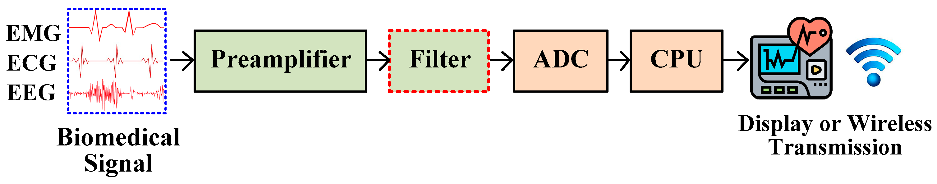
1. Introduction
2. Proposed Circuit
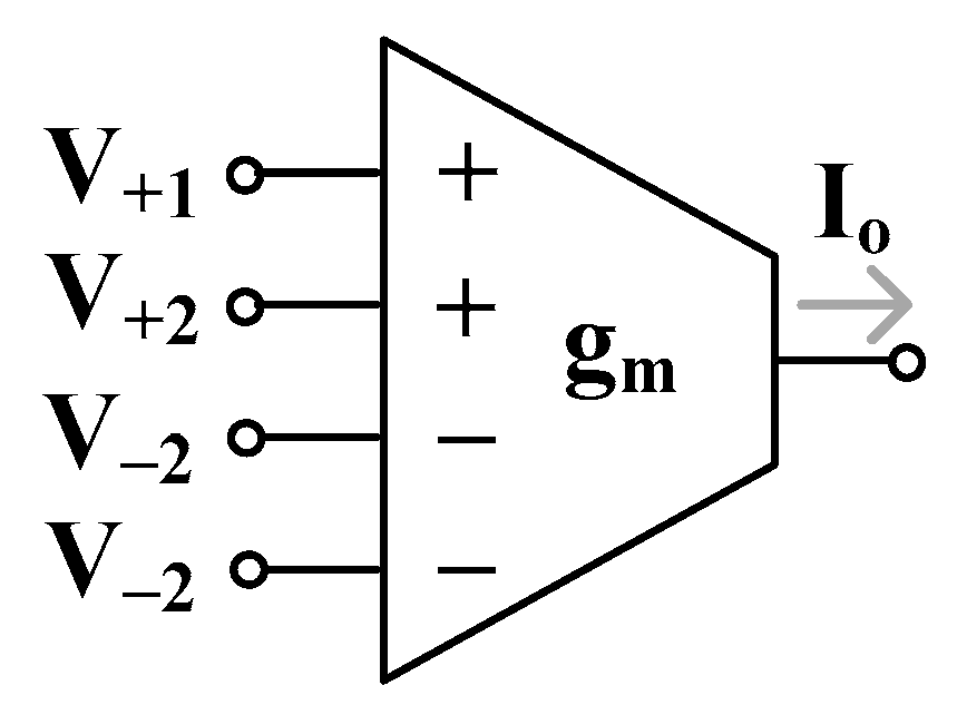
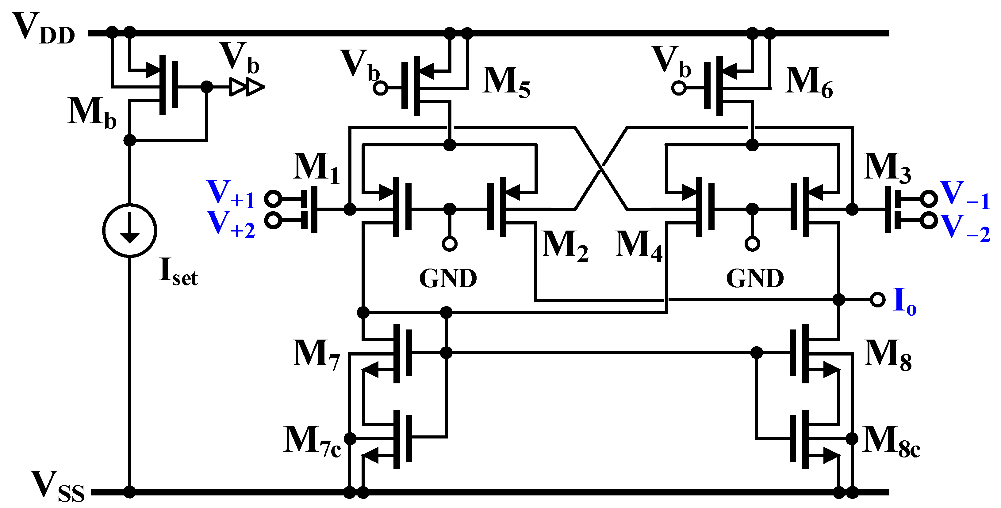
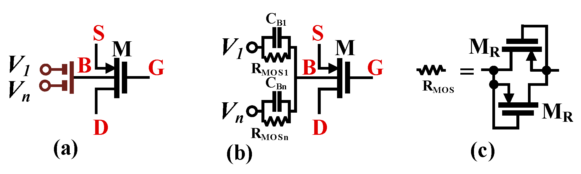
2.1. MI-OTA
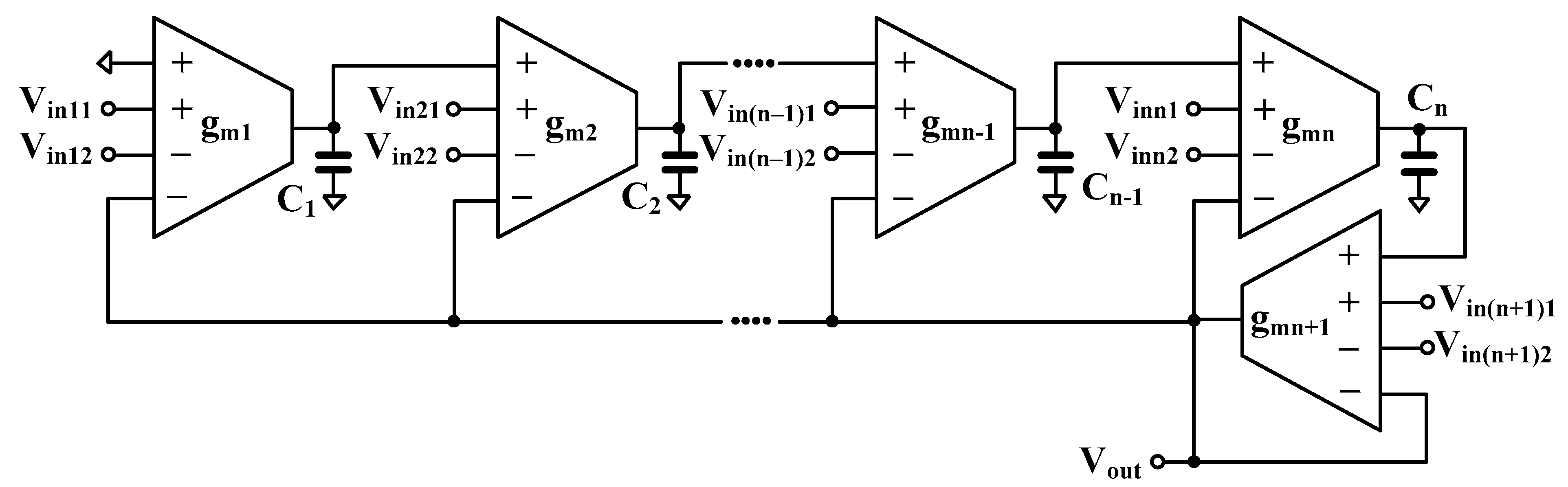
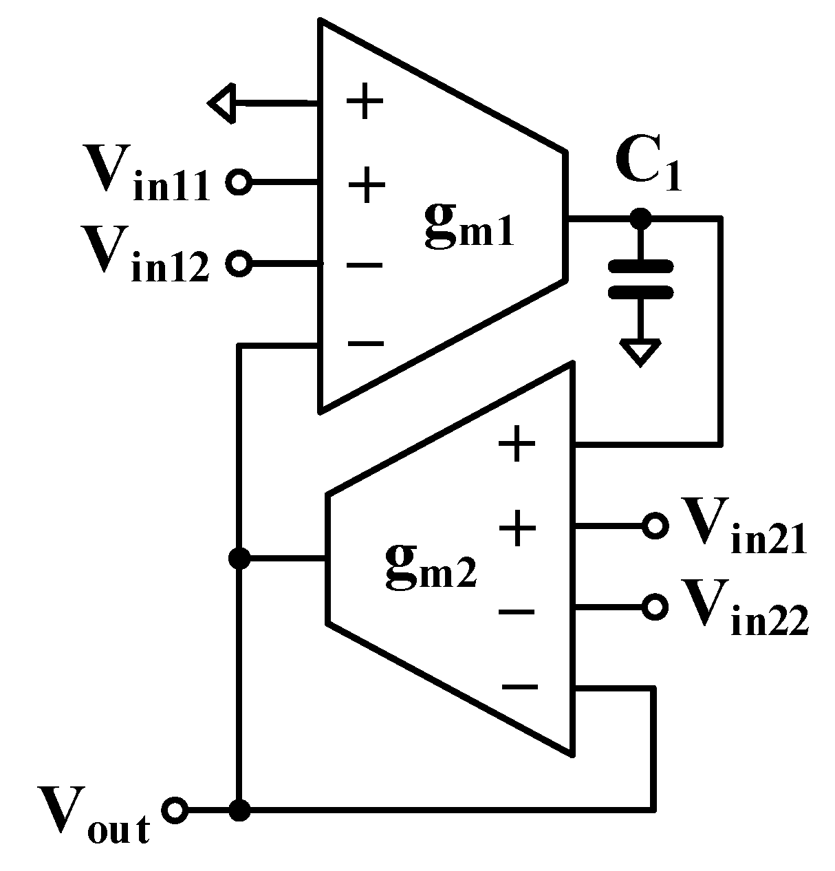
2.2. Proposed High-Order Universal Filter
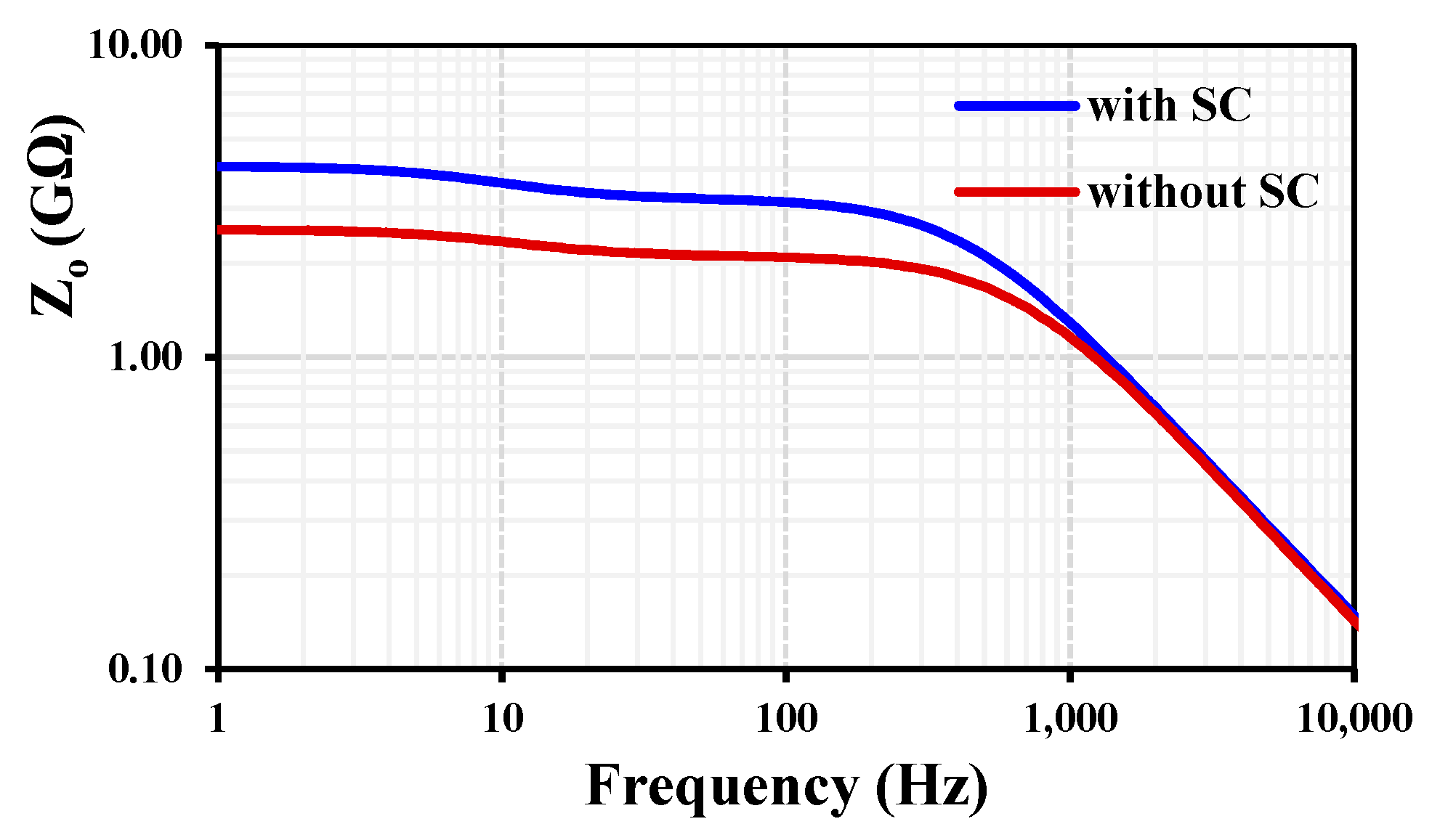
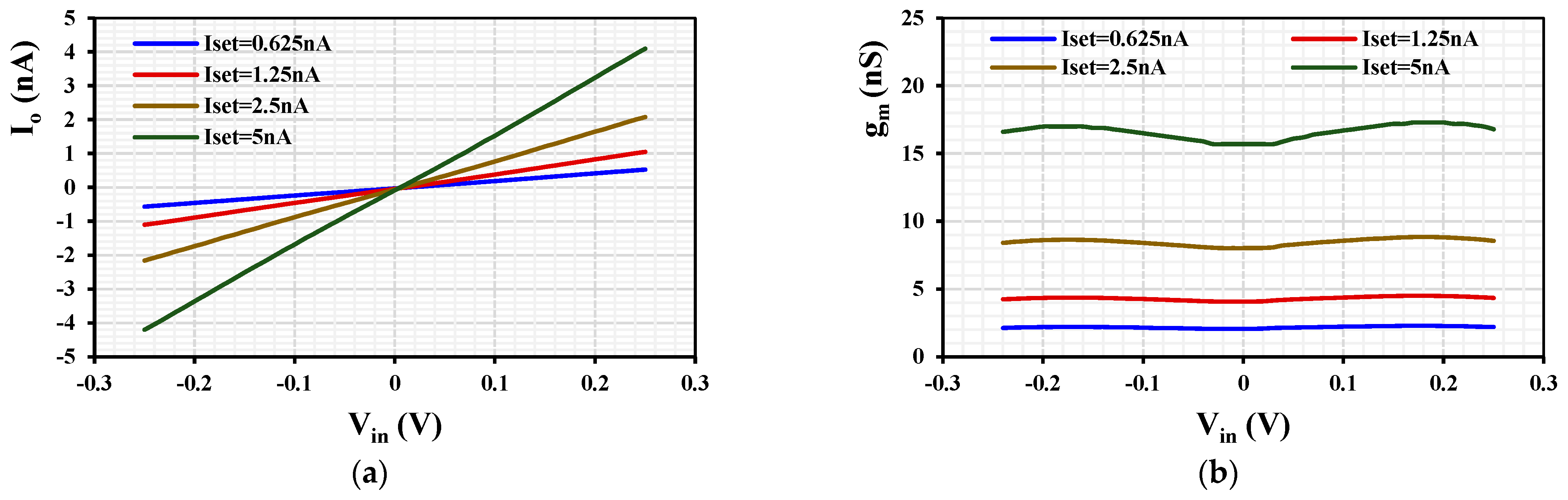
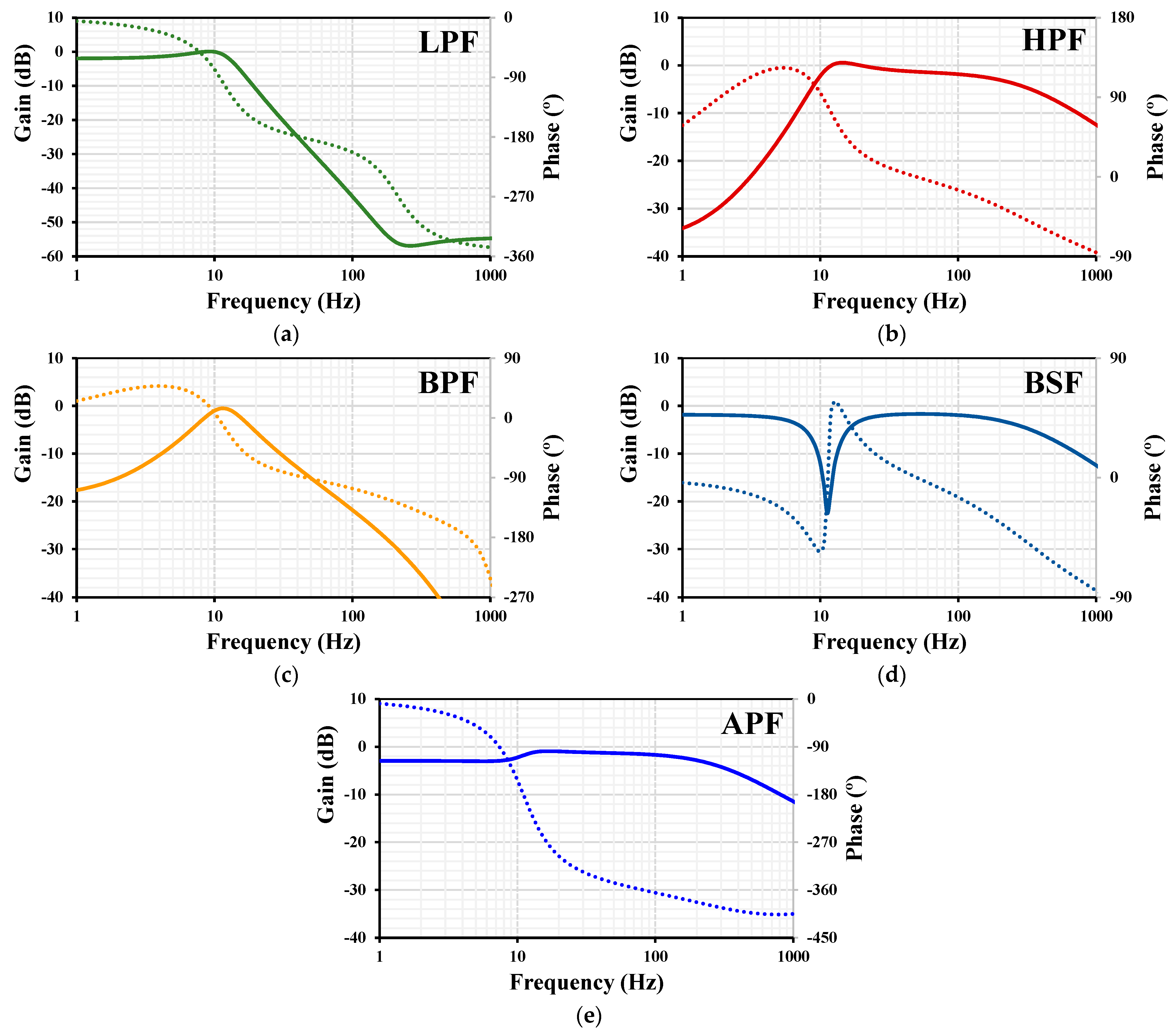
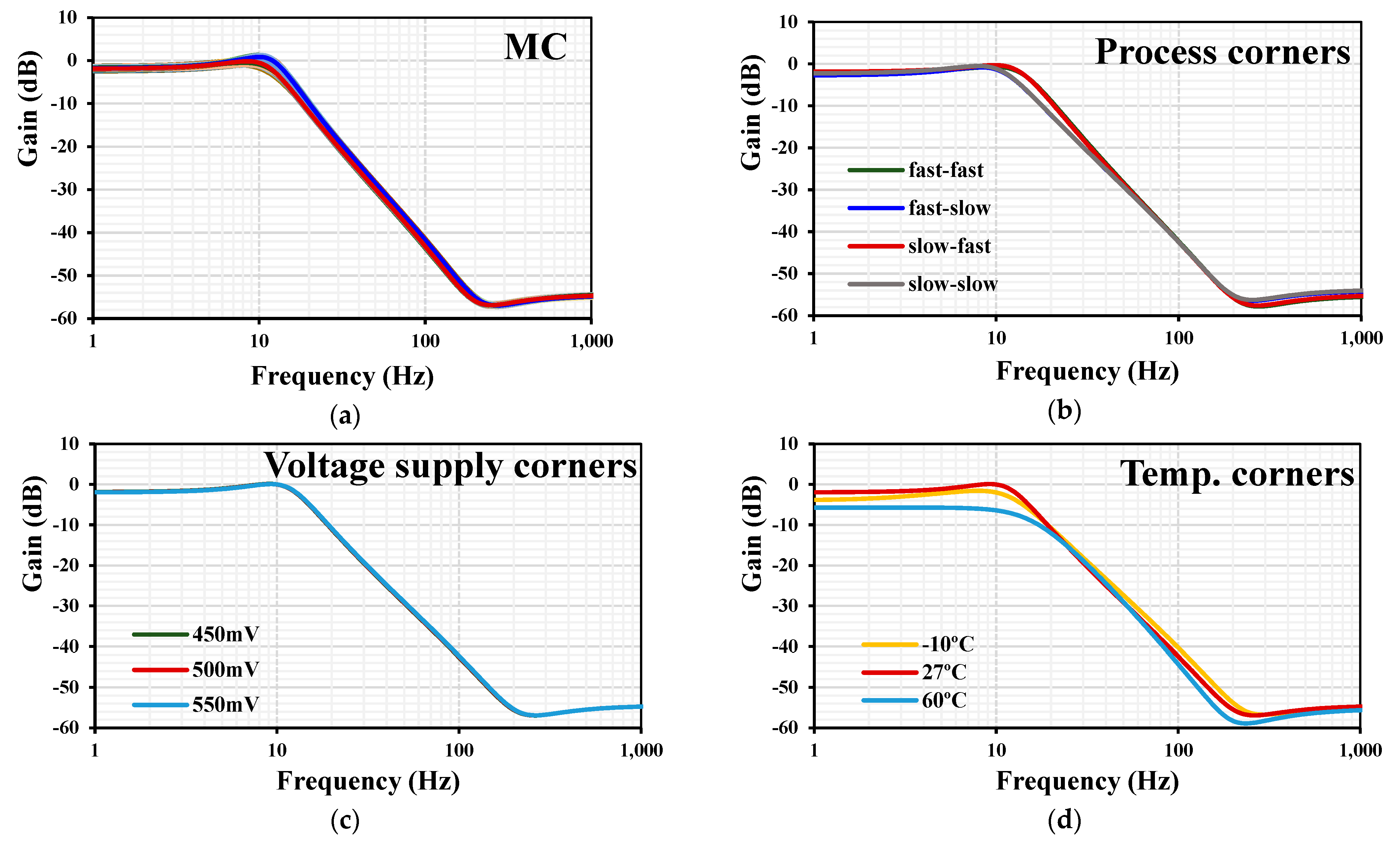
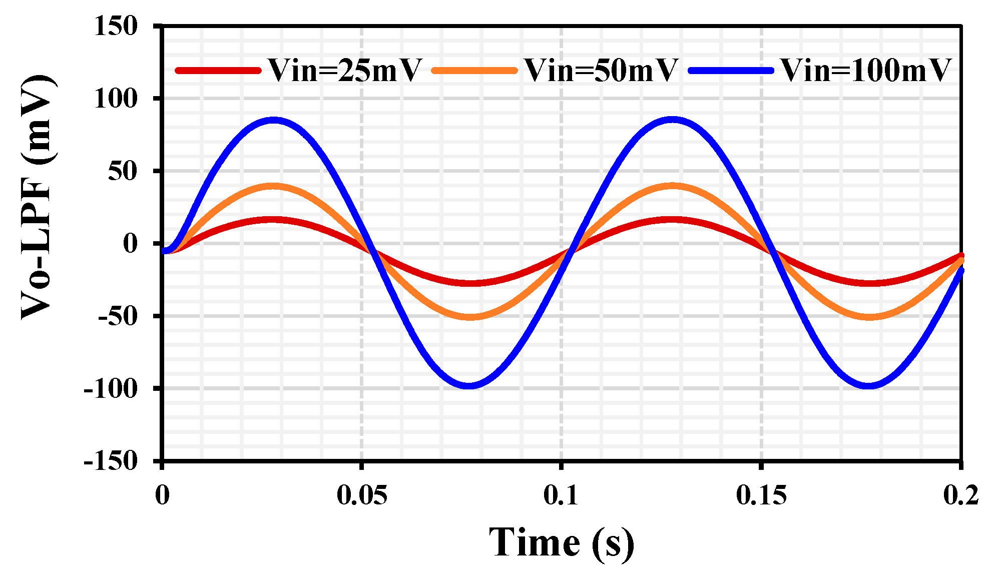
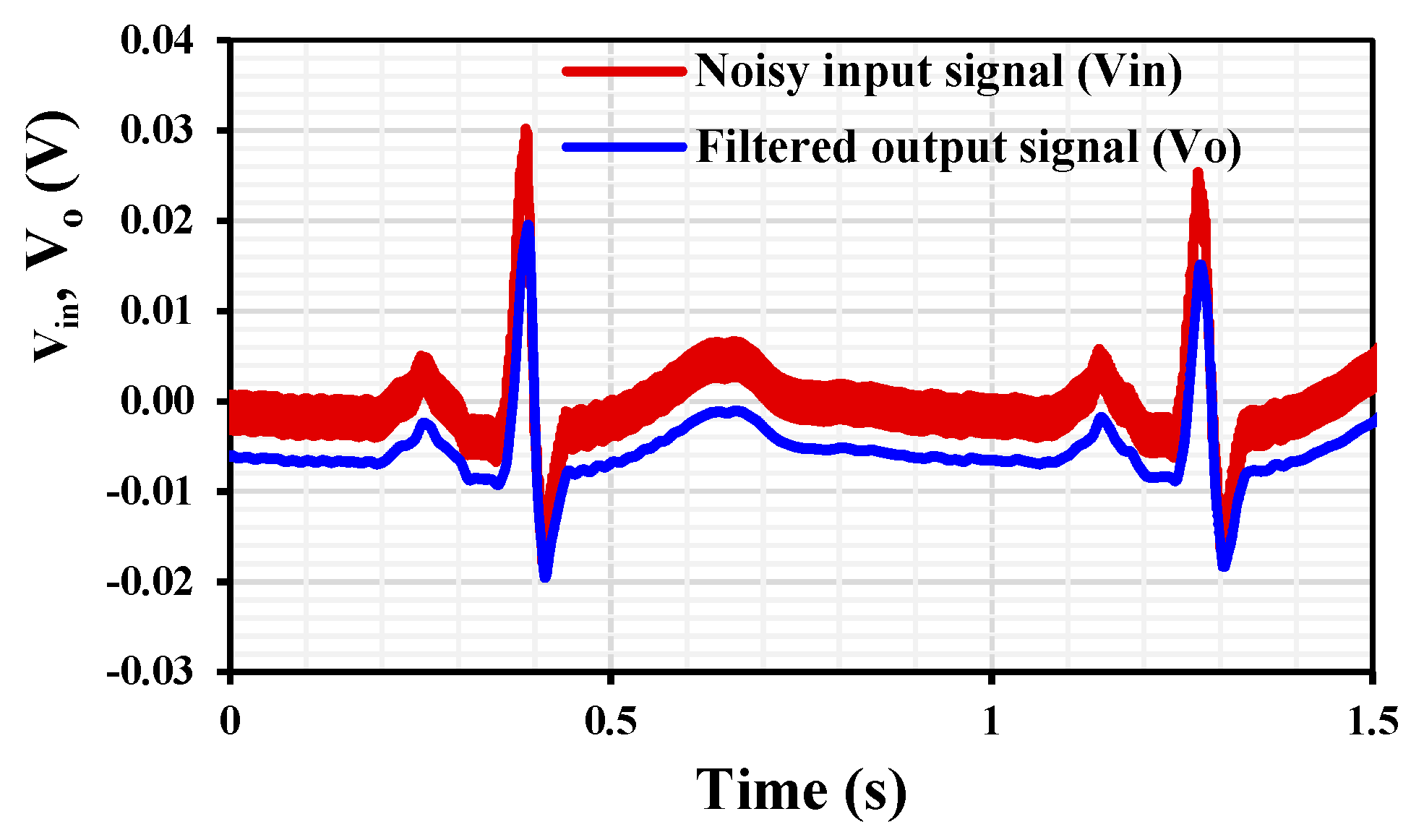
3. Simulation Results
4. Conclusions
Author Contributions
Funding
Institutional Review Board Statement
Informed Consent Statement
Data Availability Statement
Conflicts of Interest
References
- Webster, J.G. Medical Instrumentation: Application and Design, 4th ed.; John Wiley & Sons: Hoboken, NJ, USA, 2010; pp. 11–12. [Google Scholar]
- Lee, S.-Y.; Cheng, C.-J. Systematic Design and Modeling of a OTA-C Filter for Portable ECG Detection. IEEE Trans. Biomed. Circuits Syst. 2009, 3, 53–64. [Google Scholar] [CrossRef] [PubMed]
- Yang, M.; Liu, J.; Xiao, Y.; Liao, H. 14.4 nW Fourth-Order Bandpass Filter for Biomedical Applications. Electron. Lett. 2010, 46, 973–974. [Google Scholar] [CrossRef]
- Thomas, C.W.; Huebner, W.P.; Leigh, R.J. A Low-Pass Notch Filter for Bioelectric Signals. IEEE Trans. Biomed. Eng. 1988, 35, 496–498. [Google Scholar] [CrossRef] [PubMed]
- van Dijk, L.P.L.; van der Woerd, A.C.; Mulder, J.; van Roermund, A.H.M. An ultra-low-power, low-voltage electronic audio delay line for use in hearing aids. IEEE J. Solid-State Circuits 1998, 33, 291–294. [Google Scholar] [CrossRef]
- Wang, R.; Jin, C.; McEwan, A.; van Schaik, A. A programmable axonal propagation delay circuit for time-delay spiking neural networks. In Proceedings of the 2011 IEEE International Symposium of Circuits and Systems (ISCAS), Rio de Janeiro, Brazil, 15–18 May 2011; pp. 869–872. [Google Scholar] [CrossRef]
- Rodriguez-Villegas, E.; Casson, A.J.; Corbishley, P. A Subhertz Nanopower Low-Pass Filter. IEEE Trans. Circuits Syst. II Express Briefs 2011, 58, 351–355. [Google Scholar] [CrossRef]
- Paul, A.; Ramírez-Angulo, J.; Lopez-Martin, A.J.; Carvajal, R.G. CMOS First-Order All-Pass Filter With 2-Hz Pole Frequency. IEEE Trans. Very Large Scale Integr. (VLSI) Syst. 2019, 27, 294–303. [Google Scholar] [CrossRef]
- Martincorena-Arraiza, M.; De La Cruz-Blas, C.A.; Lopez-Martin, A.; Carlosena, A. Micropower Class AB Low-Pass Analog Filter Based on the Super-Source Follower. IEEE Trans. Circuits Syst. II Express Briefs 2022, 69, 3684–3688. [Google Scholar] [CrossRef]
- Carrillo, J.M.; de la Cruz-Blas, C.A. 0.6-V 1.65-μW Second-Order Gm-C Bandpass Filter for Multi-Frequency Bioimpedance Analysis Based on a Bootstrapped Bulk-Driven Voltage Buffer. J. Low Power Electron. Appl. 2022, 12, 62. [Google Scholar] [CrossRef]
- Corbacho, I.; Carrillo, J.M.; Ausín, J.L.; Domínguez, M.A.; Pérez-Aloe, R.; Duque-Carrillo, J.F. CMOS Widely Tunable Second-Order Gm-C Bandpass Filter for Multi-Sine Bioimpedance Analysis. Electronics 2023, 12, 1326. [Google Scholar] [CrossRef]
- Yin, Y.; Zhang, X.; Feng, Z.; Qi, H.; Lu, H.; He, J.; Jin, C.; Luo, Y. An Ultra-Low-Voltage Transconductance Stable and Enhanced OTA for ECG Signal Processing. Micromachines 2024, 15, 1108. [Google Scholar] [CrossRef]
- Namdari, A.; Aiello, O.; Caviglia, D.D. A 0.5 V, 32 nW Compact Inverter-Based All-Filtering Response Modes Gm-C Filter for Bio-Signal Processing. J. Low Power Electron. Appl. 2024, 14, 40. [Google Scholar] [CrossRef]
- Deo, A.; Pandey, S.K.; Joshi, A.; Sharma, S.K.; Shrimali, H. Design of a Third Order Butterworth Gm-C Filter for EEG Signal Detection Application. In Proceedings of the 2018 25th International Conference “Mixed Design of Integrated Circuits and System” (MIXDES), Gdynia, Poland, 21–23 June 2018; pp. 361–365. [Google Scholar] [CrossRef]
- Diab, M.S.; Mahmoud, S.A. Balanced OTA-C Elliptic Cauer Filters for Biomedical Applications. In Proceedings of the 2018 41st International Conference on Telecommunications and Signal Processing (TSP), Athens, Greece, 4–6 July 2018; pp. 1–5. [Google Scholar] [CrossRef]
- Fujii, T.; Matsumoto, F.; Shouno, K. Very Low Frequency Lowpass Filter with Finite Transmission Zeros Realized by Using Extended Symmetrical Impedance Scaling Circuit. In Proceedings of the 2019 34th International Technical Conference on Circuits/Systems, Computers and Communications (ITC-CSCC), JeJu, Republic of Korea, 23–26 June 2019; pp. 1–4. [Google Scholar] [CrossRef]
- Rajan, V.S.; Venkataramani, B. Design of Low Power, Programmable Low-Gm OTAs and Gm-C Filters for Biomedical Applications. Analog Integr. Circuits Signal Process. 2021, 107, 389–409. [Google Scholar] [CrossRef]
- Krishna, M.; Laxminidhi, T. Widely Tunable Lowpass gm-C Filter for Biomedical Applications. IET Circuits Devices Syst. 2019, 13, 239–244. [Google Scholar] [CrossRef]
- Alhammadi, A.A.; Mahmoud, S.A. Fully differential fifth-order dual-notch power line interference filter oriented to EEG detection system with low pass feature. Microelectron. J. 2016, 56, 122–133. [Google Scholar] [CrossRef]
- Sun, C.-Y.; Lee, S.-Y. A Fifth-Order Butterworth OTA-C LPF with Multiple-Output Differential-Input OTA for ECG Applications. IEEE Trans. Circuits Syst. II Express Briefs 2018, 65, 421–425. [Google Scholar] [CrossRef]
- Lee, S.-Y.; Wang, C.-P.; Chu, Y.-S. Low-Voltage OTA-C Filter with an Area- and Power-Efficient OTA for Biosignal Sensor Applications. IEEE Trans. Biomed. Circuits Syst. 2019, 13, 56–67. [Google Scholar] [CrossRef]
- Pinto, P.M.; Ferreira, L.H.C.; Colletta, G.D.; Braga, R.A.A. A 0.25-V fifth-order Butterworth low-pass filter based on fully differential difference transconductance amplifier architecture. Microelectron. J. 2019, 92, 104606. [Google Scholar] [CrossRef]
- Castello, R.; Grassi, A.G.; Donati, S. A 500-nA sixth-order bandpass SC filter. IEEE J. Solid-State Circuits 1990, 25, 669–676. [Google Scholar] [CrossRef]
- Solis-Bustos, S.; Silva-Martinez, J.; Maloberti, F.; Sanchez-Sinencio, E. A 60-dB dynamic-range CMOS sixth-order 2.4-Hz low-pass filter for medical applications. IEEE Trans. Circuits Syst. II Analog Digit. Signal Process. 2000, 47, 1391–1398. [Google Scholar] [CrossRef]
- Corbishley, P.; Rodriguez-Villegas, E. A Nanopower Bandpass Filter for Detection of an Acoustic Signal in a Wearable Breathing Detector. IEEE Trans. Biomed. Circuits Syst. 2007, 1, 163–171. [Google Scholar] [CrossRef]
- Bertsias, P.; Psychalinos, C. Ultra-Low Voltage Sixth-Order Low Pass Filter for Sensing the T-Wave Signal in ECGs. J. Low Power Electron. Appl. 2014, 4, 292–303. [Google Scholar] [CrossRef]
- Gosselin, B.; Sawan, M.; Kerherve, E. Linear-Phase Delay Filters for Ultra-Low-Power Signal Processing in Neural Recording Implants. IEEE Trans. Biomed. Circuits Syst. 2010, 4, 171–180. [Google Scholar] [CrossRef]
- Horng, J.-W. Analytical synthesis of general high-order voltage/current transfer functions using CCIIs. Microelectron. J. 2012, 43, 546–554. [Google Scholar] [CrossRef]
- Jiang, J.; Zhou, X.; Xu, W. Nth-order current transfer function synthesis using DVCCs: Signal-flow graph approach. Int. J. Electron. 2013, 100, 482–496. [Google Scholar] [CrossRef]
- Chang, C.-M.; Swamy, M.N.S.; Soliman, A.M. Analytical synthesis of voltage-mode even/odd-nth-order differential difference current conveyor and fully differential current conveyor II-grounded resistor and capacitor universal filter structures. Int. J. Circuit Theory Appl. 2015, 43, 1263–1310. [Google Scholar] [CrossRef]
- Tran, H.-D.; Wang, H.-Y.; Lin, M.-C.; Nguyen, Q.-M. Synthesis of Cascadable DDCC-Based Universal Filter Using NAM. Appl. Sci. 2015, 5, 320–343. [Google Scholar] [CrossRef]
- Choubey, C.K.; Paul, S.K. Nth order voltage-mode universal filter employing only plus type differential difference current conveyor. Analog Integr. Circuits Signal Process. 2022, 110, 197–210. [Google Scholar] [CrossRef]
- Wang, C.; Zhang, J.; Wang, L.; Shi, W.; Jing, D. A novel Nth-order voltage-mode universal filter based on CMOS CFOA. Optik 2016, 127, 2226–2230. [Google Scholar] [CrossRef]
- Kumar, A.; Paul, S.K. Nth order current mode universal filter using MOCCCIIs. Analog Integr. Circuits Signal Process. 2018, 95, 181–193. [Google Scholar] [CrossRef]
- Lee, C.-N.; Chang, C.-M. High-order mixed-mode OTA-C universal filter. AEU-Int. J. Electron. Commun. 2009, 63, 517–521. [Google Scholar] [CrossRef]
- Chang, C.-M.; Swamy, M.N.S. Analytical synthesis and comparison of voltage-mode Nth-order OTA-C universal filter structures. Int. J. Circuit Theory Appl. 2012, 40, 405–438. [Google Scholar] [CrossRef]
- Jeshvaghani, M.A.; Dolatshahi, M. A low-power multi-mode and multi-output high-order CMOS universal Gm-C filter. Analog Integr. Circuits Signal Process. 2014, 79, 95–104. [Google Scholar] [CrossRef]
- Namdari, A.; Dolatshahi, M.; Horestani, M.A. New Ultra-Low-Power High-Order Universal OTA-C Filter Based on CMOS Double Inverters in the Subthreshold Region. Circuits Syst. Signal Process. 2023, 42, 6379–6398. [Google Scholar] [CrossRef]
- Zhang, Y.; Zhao, W. A 392-pW 42.7-dB Gm-C wavelet filter for low-frequency feature extraction used for wearable sensor. Analog Integr. Circuits Signal Process. 2021, 109, 335–344. [Google Scholar] [CrossRef]
- Nako, J.; Psychalinos, C.; Elwakil, A.S.; Jurisic, D. Design of Higher-Order Fractional Filters with Fully Controllable Frequency Characteristics. IEEE Access 2023, 11, 43205–43215. [Google Scholar] [CrossRef]
- Tanimoto, H.; Koyama, M.; Yoshida, Y. Realization of a 1-V active filter using a linearization technique employing plurality of emitter-coupled pairs. IEEE J. Solid-State Circuits 1991, 26, 937–945. [Google Scholar] [CrossRef]
- Furth, P.M.; Andreou, A.G. Linearized differential transconductors in subthreshold CMOS. Electron. Lett 1995, 31, 545–547. [Google Scholar] [CrossRef]
- Khateb, F.; Kulej, T.; Kumngern, M.; Psychalinos, C. Multiple-input bulk-driven MOS transistor for low-voltage low-frequency applications. Circuits Syst. Signal Process 2019, 38, 2829–2845. [Google Scholar] [CrossRef]
- Khateb, F.; Kulej, T.; Akbari, M.; Tang, K.-T. A 0.5-V multiple-input bulk-driven OTA in 0.18-μm CMOS. IEEE Trans. Very Large Scale Integr. (VLSI) Syst. 2022, 30, 1739–1747. [Google Scholar] [CrossRef]


| Filtering Function | Input | Transfer Function | |
|---|---|---|---|
| LPF | Non-inverting | ||
| Inverting | |||
| HPF | Non-inverting | ||
| Inverting | |||
| APF | Non-inverting | ||
| Inverting | |||
| Filtering Function | Input | Transfer Function | |
|---|---|---|---|
| HPF | Non-inverting | ||
| Inverting | |||
| BPF | Non-inverting | ||
| Inverting | |||
| LPF | Non-inverting | ||
| Inverting | |||
| BSF | Non-inverting | ||
| Inverting | |||
| APF | Non-inverting | ||
| Inverting | |||
| Filtering Function | Input | Transfer Function | |
|---|---|---|---|
| HPF | Non-inverting | ||
| Inverting | |||
| BPF1 | Non-inverting | ||
| Inverting | |||
| BPF2 | Non-inverting | ||
| Inverting | |||
| LPF | Non-inverting | ||
| Inverting | |||
| APF | Non-inverting | ||
| Inverting | |||
| Component | W/L (µm/µm) |
|---|---|
| M1, M3 | 37.5/1 |
| M2, M4 | 10/1 |
| M7, M7c, M8, M8c | 30/1 |
| Mb, M5, M6 | 15/1 |
| MR | 4/5 |
| CB = 0.5 pF | |
| Factor | Proposed | [12] 2024 | [13] 2024 | [32] 2022 | [38] 2023 |
|---|---|---|---|---|---|
| Realization | 180 nm | 180 nm | 180 nm | 180 nm | 180 nm |
| Order | 2 | 2 | 2 | 3 | 2 |
| Number of active devices | 3-OTA | 3-OTA | 3-OTA | 3-DDCC | 3-OTA |
| Number of passive devices | 2 C | 2-C | 2-C | 2 C, 3-R | 2 C |
| Type of filter | MISO | MISO | MISO | MISO | MISO |
| Operation mode | VM | VM | MM | VM | MM |
| Number of offered responses | 10 | 2 (LPF) | 5 (VM) 20 (MM) | 5 | 5 (VM) 20 (MM) |
| Yes | Yes | Yes | No | Yes | |
| No need for inverted input signal | Yes | Yes | No | No | No |
| Natural frequency (Hz) | 11 | 250 | 462 | 158.7 × 10³ | 14 × 103 |
| Voltage supply (V) | 0.5 | 0.4 | 0.5 | ±0.9 | ±0.5 |
| ) | 2.81 | 20.5 | 32 | 143 × 103 | 429 |
| THD (%) | 2@200 mVpp | - | <2@40 mVpp | - | 1@200 mVpp |
| Dynamic range (dB) | 54.4 | 41.5 | 43.59 | - | 63.18 |
| 2.3 × 10⁻¹² | 3.45 × 10⁻¹³ | 0.229 × 10⁻¹² | - | 0.01 × 10⁻¹² | |
| Verification of result | Sim | Post-sim | Sim | Sim | Post-sim |
Disclaimer/Publisher’s Note: The statements, opinions and data contained in all publications are solely those of the individual author(s) and contributor(s) and not of MDPI and/or the editor(s). MDPI and/or the editor(s) disclaim responsibility for any injury to people or property resulting from any ideas, methods, instructions or products referred to in the content. |
© 2025 by the authors. Licensee MDPI, Basel, Switzerland. This article is an open access article distributed under the terms and conditions of the Creative Commons Attribution (CC BY) license (https://creativecommons.org/licenses/by/4.0/).
Share and Cite
Kumngern, M.; Khateb, F.; Kulej, T.; Lerkvaranyu, S. 0.5-V High-Order Universal Filter for Bio-Signal Processing Applications. Appl. Sci. 2025, 15, 3969. https://doi.org/10.3390/app15073969
Kumngern M, Khateb F, Kulej T, Lerkvaranyu S. 0.5-V High-Order Universal Filter for Bio-Signal Processing Applications. Applied Sciences. 2025; 15(7):3969. https://doi.org/10.3390/app15073969
Chicago/Turabian StyleKumngern, Montree, Fabian Khateb, Tomasz Kulej, and Somkiat Lerkvaranyu. 2025. "0.5-V High-Order Universal Filter for Bio-Signal Processing Applications" Applied Sciences 15, no. 7: 3969. https://doi.org/10.3390/app15073969
APA StyleKumngern, M., Khateb, F., Kulej, T., & Lerkvaranyu, S. (2025). 0.5-V High-Order Universal Filter for Bio-Signal Processing Applications. Applied Sciences, 15(7), 3969. https://doi.org/10.3390/app15073969