1. Introduction
Vision is crucial for transferring information from the external environment to the brain. It accounts for over 90% of all external information. Photoreceptors in the retinal layer of the eye convert photons into neural impulses that are then transferred to the brain for vision creation. Age-related macular degeneration (AMD) and retinitis pigmentosa (RP) are photoreceptor diseases that cause vision loss, night blindness, and eventually blindness.
Functional electrical stimulations (FESs) have been used extensively in human vision restoration experiments and are known to restore eyesight lost because of RP and AMD. The goal of FES is to depolarize the neuronal membrane by transferring electric charges. A crucial component of FES is controlling the electric charges and properties, such as the current value and shape of the current pulses, in order to artificially generate an action potential at the neural membrane.
Many methods have been developed as a result of the implanted electrode array’s structural site inside the retina, which can be divided into epiretinal [
1,
2,
3,
4], subretinal [
5,
6,
7,
8], and suprachoroidal [
9,
10]. High-pixel densities of up to 1600 pixels can be produced using subretinal implants [
8]. Several stimulation pulse designs [
6,
11,
12,
13,
14,
15] have been proposed to improve efficiency during stimulation, controlling power consumption, and prevent current leakage [
16,
17].
Rectangular biphasic pulses [
11,
12,
13,
14,
15,
18] have evolved as a solution to the most crucial criteria: stimulation efficiency and preventing amplitude mismatch to minimize current leakage. The size, shape, and amplitude of the current pulses must also be controlled by an implanted digital controller or a stimulus driver, as each visually impaired patient has a unique threshold for stimulating retinal neurons. An electric field is created when a charge is injected into retinal tissue through an electrode array, affecting neuron excitation. However, in high-density retinal implants where electrodes are closely spaced, electrical crosstalk between them can occur during stimulation, which may activate unwanted retinal cells. This results in blurred images for patients [
19,
20,
21,
22,
23]. Thus, it is essential to design a digital controller that can mitigate the disadvantages of crosstalk.
Most retinal implants have employed a single reference electrode, resulting in a greater separation between the active and reference electrodes. Consequently, the electric charge during stimulation flows from the activated electrode to the single reference electrode, which is placed farther away. This phenomenon can trigger undesirable excitation in retinal tissues. Clinically, it has been reported that the density of the electrode array is directly proportional to improvements in visual acuity [
24,
25]. Therefore, it is essential to position the reference electrode close to the activated electrode.
For high-density retinal implants, the electrical stimulation protocol, adjusted by a digital controller, must also meet the design requirement for flicker-free vision frequency [
26]. This means that several electrodes are activated simultaneously, resulting in instantaneous high-power dissipation. Therefore, a digital controller capable of generating stimulation pulse trains should be designed to both reduce power consumption and meet the flicker-free vision frequency of 60 Hz.
This work proposes a digital controller for a 256-pixel subretinal implant to reduce the crosstalk effects caused by the increased number of pixels. By employing a hexagonal electrode structure, the reference electrode, typically located far away, can be placed near the activated electrode during stimulation, thereby eliminating undesirable excitation. In addition to the hexagonal electrode structure, an overlapping stimulation method can meet the flicker-free vision frequency and reduce power dissipation. The proposed digital controller provides the overlapping stimulation profile, which will be addressed in the next section.
In this work, 32-bit input data are transmitted wirelessly at a rate of 20 kbps, along with a 2 MHz clock, to control the hexagonal-stimulation digital controller on the receiver side. As the number of pixels increases, the time required to activate all electrodes also increases, which might affect flicker-free vision. Therefore, the proposed digital controller includes a feature to keep the time required to control the pixels within a specific range.
Our 256-pixel digital controller focuses on four key aspects:
Designing a compact external transmitter that supplies sufficient power, clock, and data to meet system requirements.
Creating a receiver digital controller that generates pulses based on the data received from the transmitter to control resolution, light intensity effects, and ensure flicker-free vision.
Generating biphasic pulses on the stimulator using signals from the digital controller.
Providing complete control over biphasic pulses to address issues of power leakage, crosstalk, and light intensity.
2. Materials and Methods
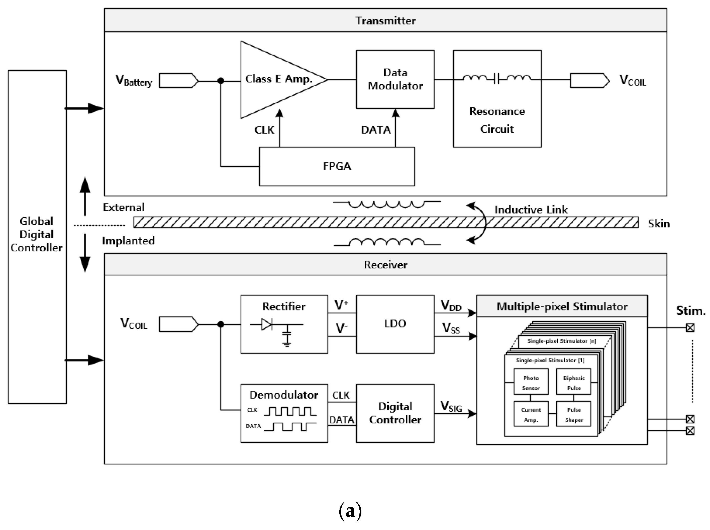
Figure 1a presents the architecture of the 256-pixel subretinal implant system, which is divided into two main components: the transmitter and the receiver. The transmitter in this study consists of a Class-E amplifier and a field-programmable gate array (FPGA). The FPGA generates 32-bit data packets at a rate of 20 kbps, with a clock frequency of 2 MHz. The 20 kbps data are modulated with the 2 MHz signal using an amplitude-shift keying (ASK) modulation scheme, and the resulting modulated waveform serves as the input to the Class-E amplifier, where it is utilized as the carrier frequency. The output signal from the Class-E amplifier is wirelessly transmitted to the implantable device via inductively coupled coils.
The received radio frequency (RF) signal is demodulated by an ASK demodulator [
27], extracting both the system clock and data, which are then sent to the digital controller. In this work, an advanced digital controller has been developed to manage the hexagonal stimulation of the 256 pixels, enabling enhanced resolution. The digital controller outputs five distinct signals (termed RST, CHR, CATH, ANO, and BAL), all of which are applied to the single-pixel stimulator using a switched capacitor current mirror technique [
13], as illustrated in
Figure 1b. Upon receiving the clock and data, the digital controller generates precise pulse patterns to produce biphasic pulses powered by the wireless power transfer system.
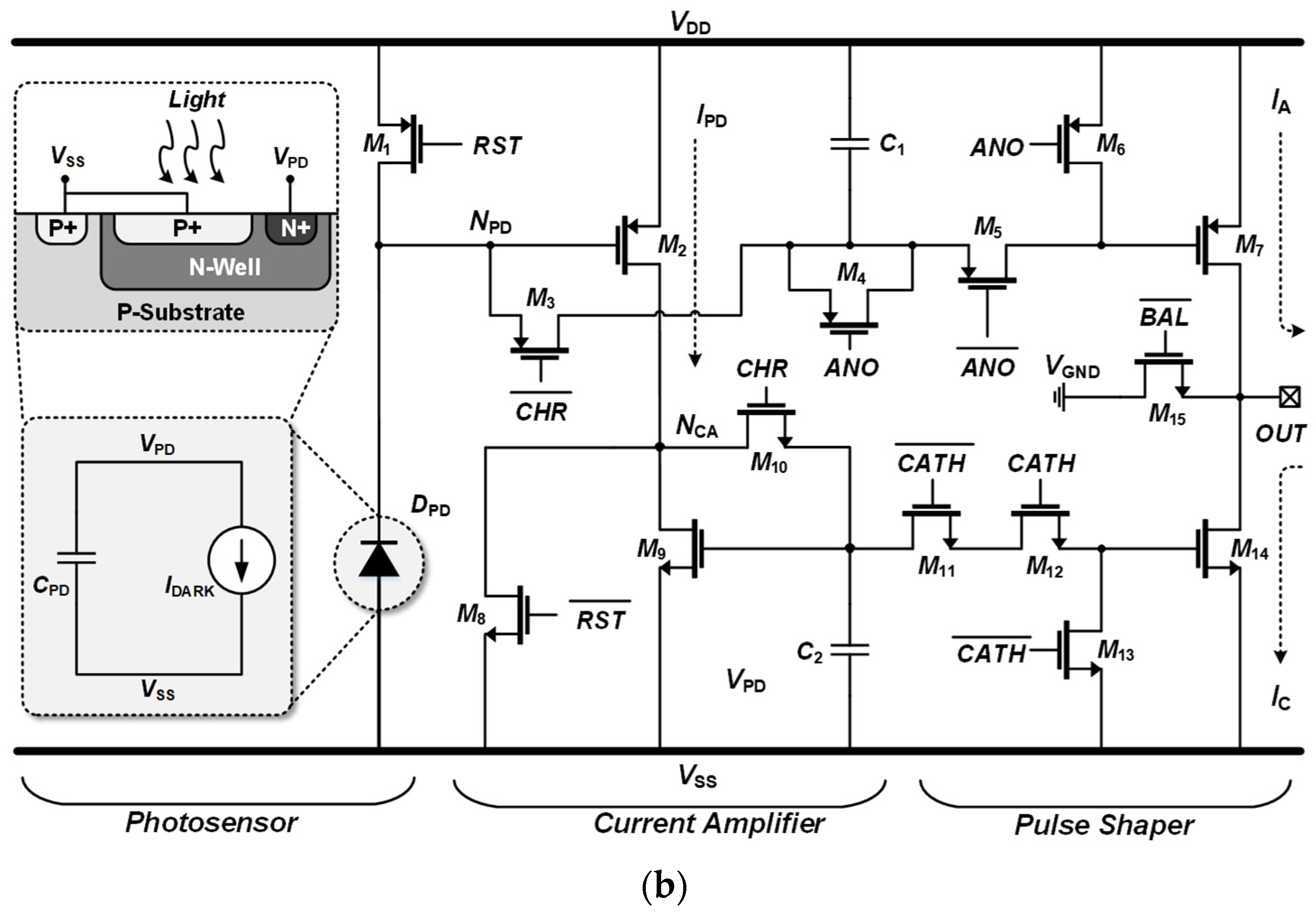
The current range for the stimulator is adjustable between 0 and 150 µA, corresponding to a light intensity range of 400–1600 lux. The photodiode generates a dark current when light is detected, and the duration of the CHR signal controls the accumulation time of this dark current on the capacitance. A longer CHR pulse duration results in a longer accumulation time, allowing for a linear response proportional to the light intensity. When the light intensity is high, the duration of the CHR pulse is minimized to regulate the amplitude of the biphasic pulse. Conversely, when the light intensity is very low or the device is in darkness, the CHR pulse is lengthened to maintain the biphasic pulse. The single-pixel stimulator, depicted in
Figure 1b, comprises a photosensor, current amplifier, and pulse shaper. It generates biphasic pulses in response to the pulse patterns determined by the digital controller based on the data received from the transmitter.
2.1. Stimulation Protocol
Controlling the current loss is a critical factor that influences ocular tissue damage. This system incorporates a digital on-chip controller that manages a hexagonal stimulator. Another essential factor of our stimulation protocol is the stimulation of the maximum number of pixels during a single phase so that total stimulation time can be reduced while achieving flicker-free vision. However, increasing the number of pixels raises the probability of crosstalk and current loss. These drawbacks are controlled by using hexagonal stimulation while applying biphasic pulses.
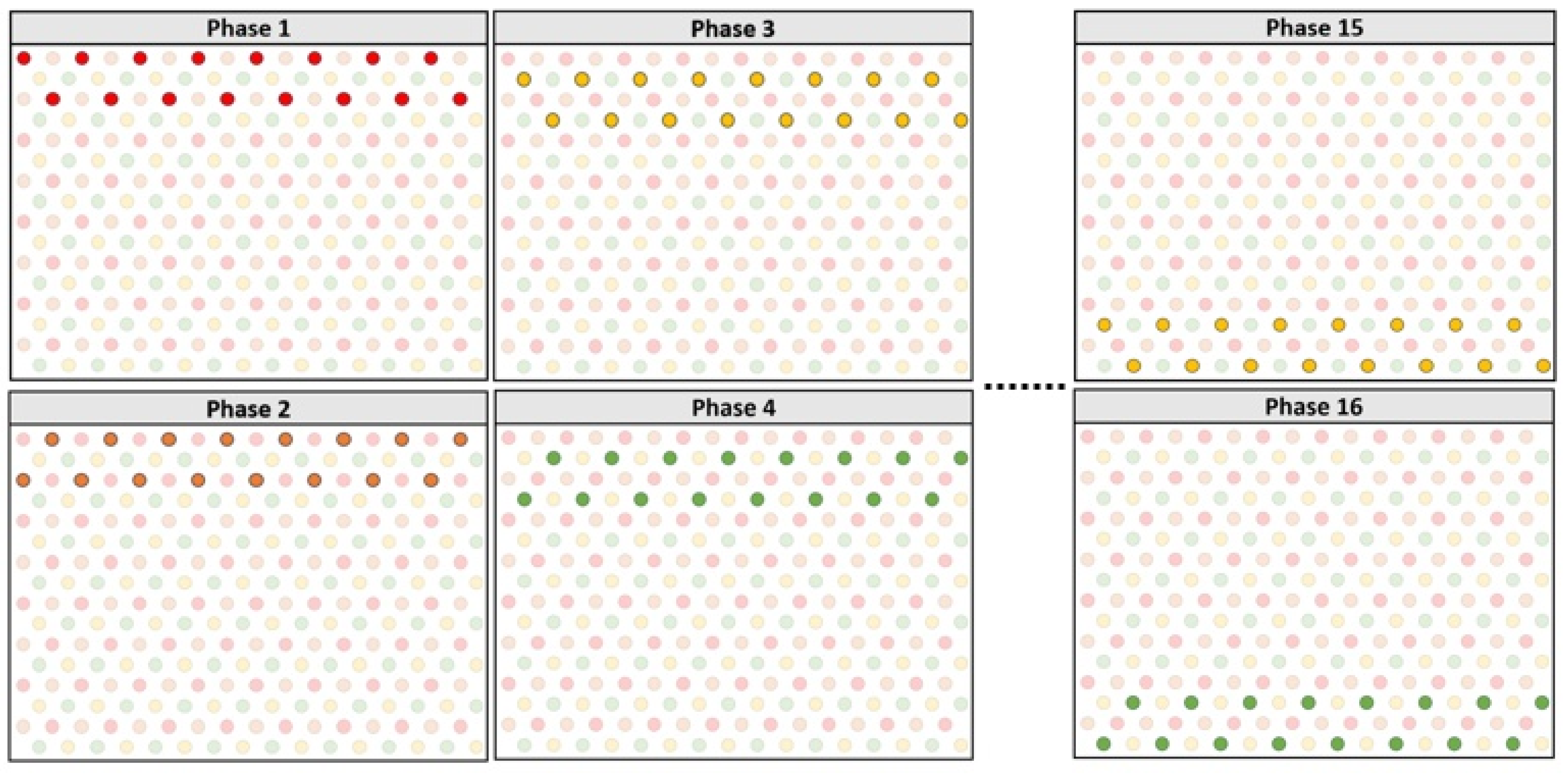
Figure 2 shows the structure of the hexagonal stimulator. The 256 electrode pixels were divided into 16 channel sets, with each set consisting of 16 pixels. Sixteen phases were used to stimulate all 256 pixels, in which 16 pixels were activated during each phase. When a single channel set was turned on for its respective time, another 16 pixels for the next phase were ready to generate a biphasic pulse with a time difference of 1 ms, which is implied during the sensing process. Sixteen pixels were excited in the first phase, along with sixteen pixels to be excited after 1 ms, and the remaining electrode pixels acted as a reference. Therefore, the technique for activating electrode pixels reduced the time required to stimulate all 256 electrode pixels.
2.2. Global Digital Controller
The transmitter and receiver are two basic systems that comprise a global digital controller, which is a part of a more extensive system. The individual system architecture of the transmitter and receiver, which serves as a global digital controller, is as follows.
2.2.1. Generating Light-Dependent Data
This system employs near-field communication to transmit data and clock signals over a wireless data telemetry system, ensuring all the devices use the same data transfer protocol. On the receiver side, these data are received and processed to form various pulse patterns, as detailed in this section.
Data should be light-dependent, and each sent data packet should reflect a specific intensity of light; this is a crucial factor when designing a transmitter. A prototype FPGA (CMOD A7) was used to generate the data for the proposed system. The data were transmitted in binary form, consisting of 0 and 1. The FPGA transmitter generated a clock at a rate of 100 MHz. On the transmitter side, the clock could be separated according to the requirements of the pulse generator. Because the entire stimulation duration may be adjusted at the transmitter side, the system is more dependable, owing to variable clock rates. For the current system, a single clock with a frequency of 2 MHz was selected.
Clock dividers were used to generate the required frequency of 2 MHz from the built-in clock of the FGPA at 100 MHz. This 2 MHz clock was output from the transmitter to the receiver through a wireless transmitter system to create pulse profiles and synchronize operations.
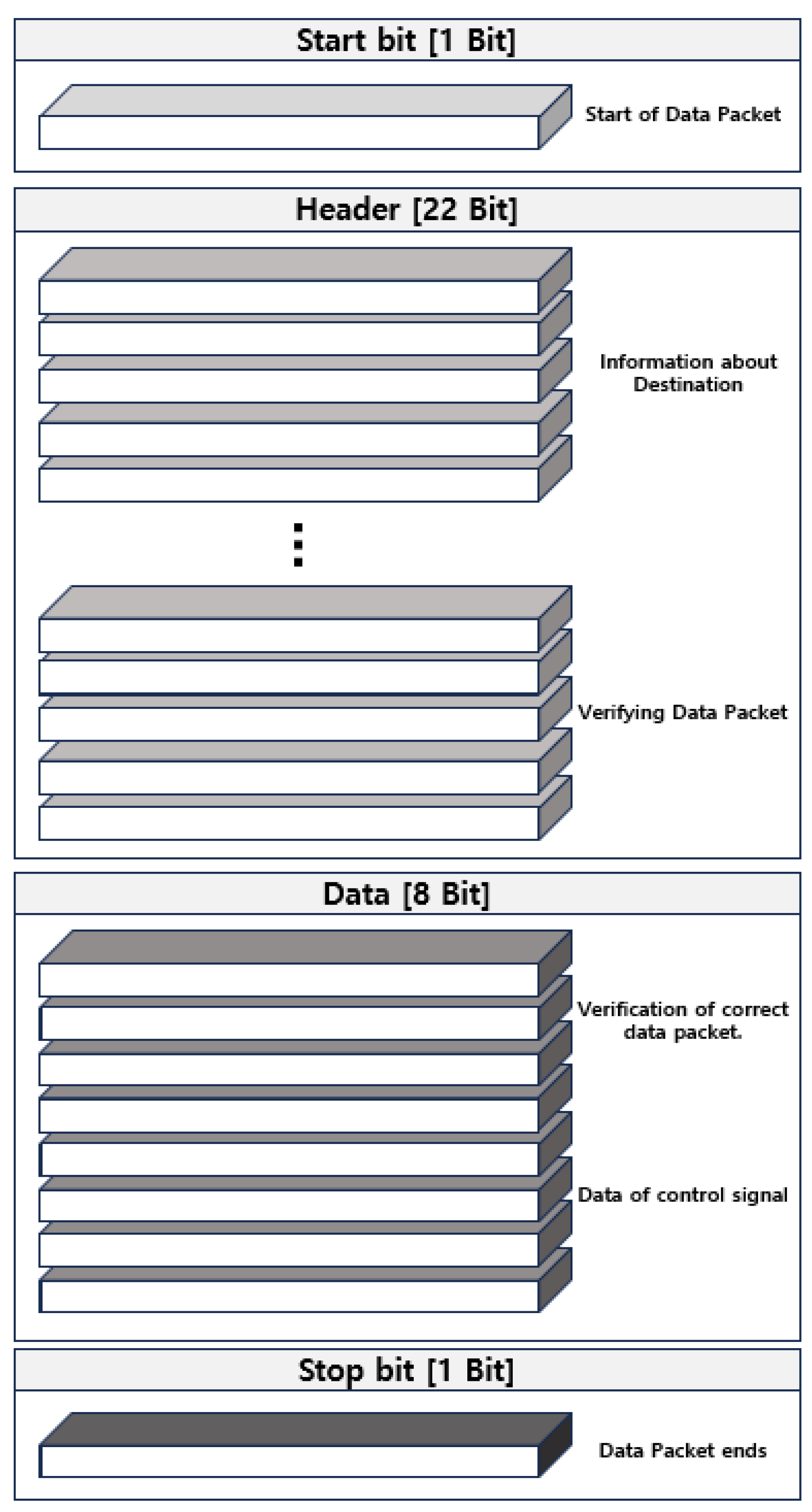
The FPGA receiver received 7-bit external data. The data were input as a series of 0 and 1, yielding 128 combinations. The form and amplitude of the biphasic pulse were determined based on each combination. The start bit, 23-bit header, and stop bit were added to the input data. The start bit marked the beginning of a new data packet. Each data pattern had its own header that contained the data address and validated the data packet. The stop bit served as parity and signified that the data packet had ended.
2.2.2. Serial Peripheral Interface Protocol
A light that passed through the FPGA generated data on the transmitter side. A unique data packet was created for data transmission, consisting of a start bit that denoted the beginning of a new packet followed by a fixed 23-bit data address. This address identified the transmitted data type and confirmed that the data packet was received correctly. The 8-bit variable data were processed immediately as the header was validated. The stop bit, which also served as the parity bit, signified the end of the data packet. The data packet structure is depicted in
Figure 3.
The data packet comprises 32 bits. Furthermore, a simple verification protocol was implemented to transmit and verify 22-bit data packets. The 8-bit binary data were generated based on the light intensity, with a starting value of 0 and a maximum value of 127. As the light intensity varied, each data value modified the form and amplitude of the pulse pattern. Furthermore, the data provided patient control over the amplitude or form of pulses elicited by electrodes inside the human eye, depending on the intensity of light.
Figure 3 shows the data packet structure. A 32-bit data packet was generated at the transmitter as parallel data using a 32-bit multiplexer. These data, along with the clock signal, were received by the receiver side. A verification protocol was applied to the serial data. This verification protocol checked for the header of each data packet, and the 8-bit data were sent to a digital controller that defines 128 different pulse patterns and amplitudes.
2.2.3. Wireless Data and Power Telemetry
Near-field communication is used for wireless communication. Inductive coils, which are standard mechanisms for transmitting wireless data and power, are used in wireless telemetry systems [
28]. The proposed system involves a Class-E power amplifier, an amplitude-shift keying modulator circuitry, and a current-sensing loop for back-telemetry-recovering data. The implanted device contained a rectifier, regulator, overvoltage protection circuit, demodulator, and reverse telemetry controller. The data were modulated on the carrier wave, which was then conveyed through an induction link, and a 2 MHz carrier frequency drove the Class-E amplifier. The impulse response was rectified before being transferred to the regulator, which generated dual-polarity voltage levels in the implanted device. The global digital controller began to operate when clock and data signals arrived from the demodulator.
2.2.4. Pulse Protocols for 256-Pixel Stimulator
The digital controller receives the signals for data and clock after processing them via a wireless data telemetry system and recovering them via a demodulator. The global digital controller uses the data and clock obtained from the transmitter to construct precise pulse patterns that will produce a biphasic pulse. In order to evaluate the entire wireless telemetry system, three platforms for the global digital controller were deployed. For the simulations, Xilinx Vivado (Version 2020.1) was employed. The outcomes were validated by hypothetical simulations on ModelSim (Version 21.1). The system was initially implemented on the FPGA to validate the global digital controller output. Data were sent and collected using FPGAs, and the findings were shown on an oscilloscope.
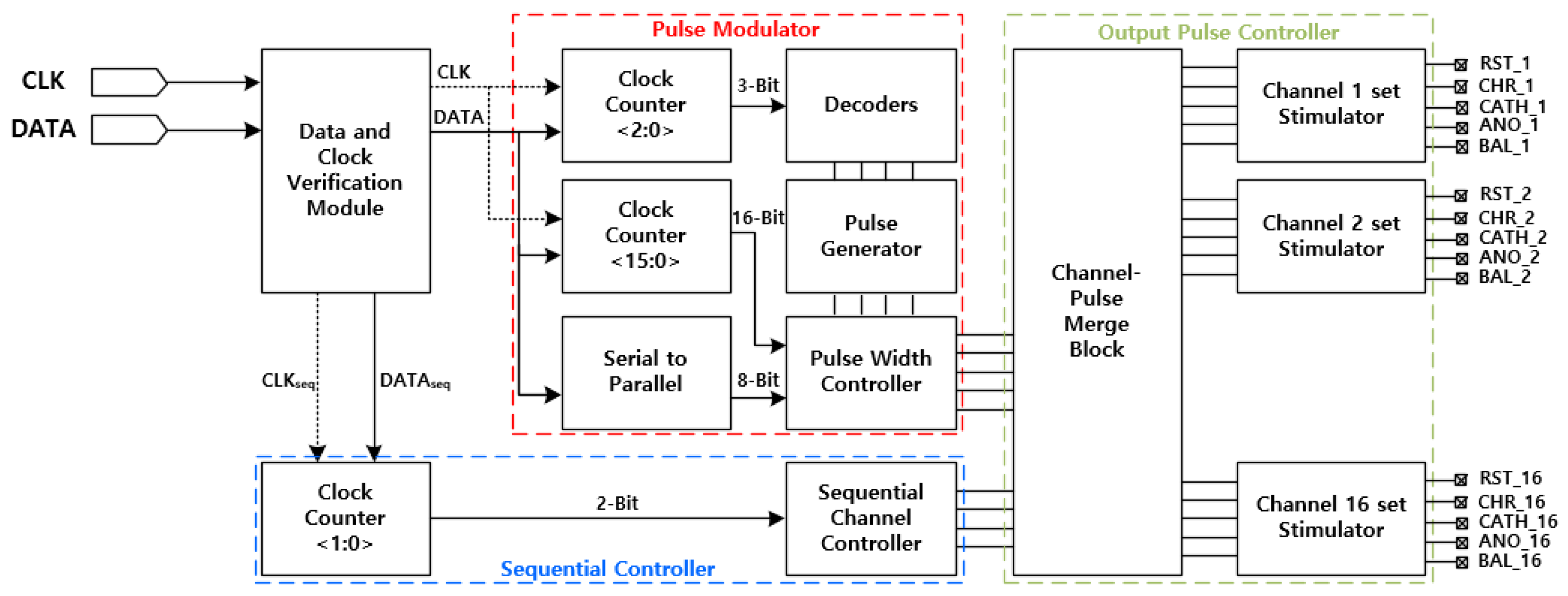
A wireless telemetry system sent the data it had received from the transmitter to the FPGA receiver. The data transmission rate of the receiver was 10 kbps, while the transmission rate of the clock was 2 MHz. The received clock was internally separated into 10 kHz clocks for data synchronization. The inside of the receiver comprises a sequential controller, pulse modulator, and output pulse controller, as shown in
Figure 4. The sequential controller determines the order of pixel channels that are activated sequentially. The pulse modulator generates a diverse pulse according to the light intensity. Finally, the output pulse controller passes the pulse information and produces suitable pulse profiles.
Pulse profiles contain five distinct signals (RST, CHR, CATH, ANO, and BAL). The RST signal serves to reset the photosensor of the single-pixel stimulator depicted in
Figure 1. The CHR is generated separately for each of the 16 channel sets based on the input light-dependent data from the transmitter side. The
signal is created at the same time that CHR is determined, and it is the inverted signal of CHR. CHR and
control the time to charge the capacitor, and the duration of charging regulates the current range between 0 and 150 µA. The CHR time is adjusted from 1 to 10 ms depending on the light intensity.
As the number of electrode pixels increases, generating flicker-free presents a challenge. Flicker-free vision in terms of a subretinal implant is defined as the time at which each electrode pixel is turned on for the next phase. The refresh rate of each electrode pixel should be within the flicker-free vision range between 20 and 50 Hz [
26]. This study proposes a design that contributes to controlling the flicker-free frequency, requiring 12 ms for each phase. Consequently, the sequential turning on of 16 channel sets could take a total time of 192 ms. In other words, the frequency is 5.20 Hz, based on Equation (1).
This rate is significantly lower than the flicker-free vision range. To prevent this, we applied an overlapping technique in which each phase starts 1 ms after the previous phase, with overlapping CHR pulses.
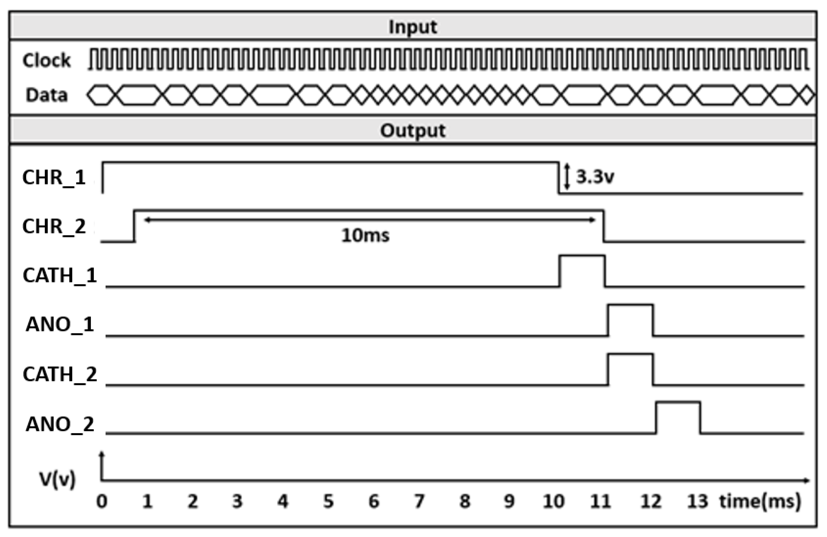
Figure 5 shows an example of overlapping current pulses for sequential channel sets. Since each CATH for the next phase starts with the ANO of the previous phase, this overlap effectively reduces the current leakage during the phase shift, and a flicker-free frequency can be achieved using the following equation:
Time for a single phase = 12 ms
Time for 16 phases starting 1 ms after the previous phase = 27 ms
Frequency = 37.03 Hz
Our system achieves a rate of 37.03 Hz.
Figure 5.
Pulse profiling of two consecutive overlapping channel sets.
Figure 5.
Pulse profiling of two consecutive overlapping channel sets.
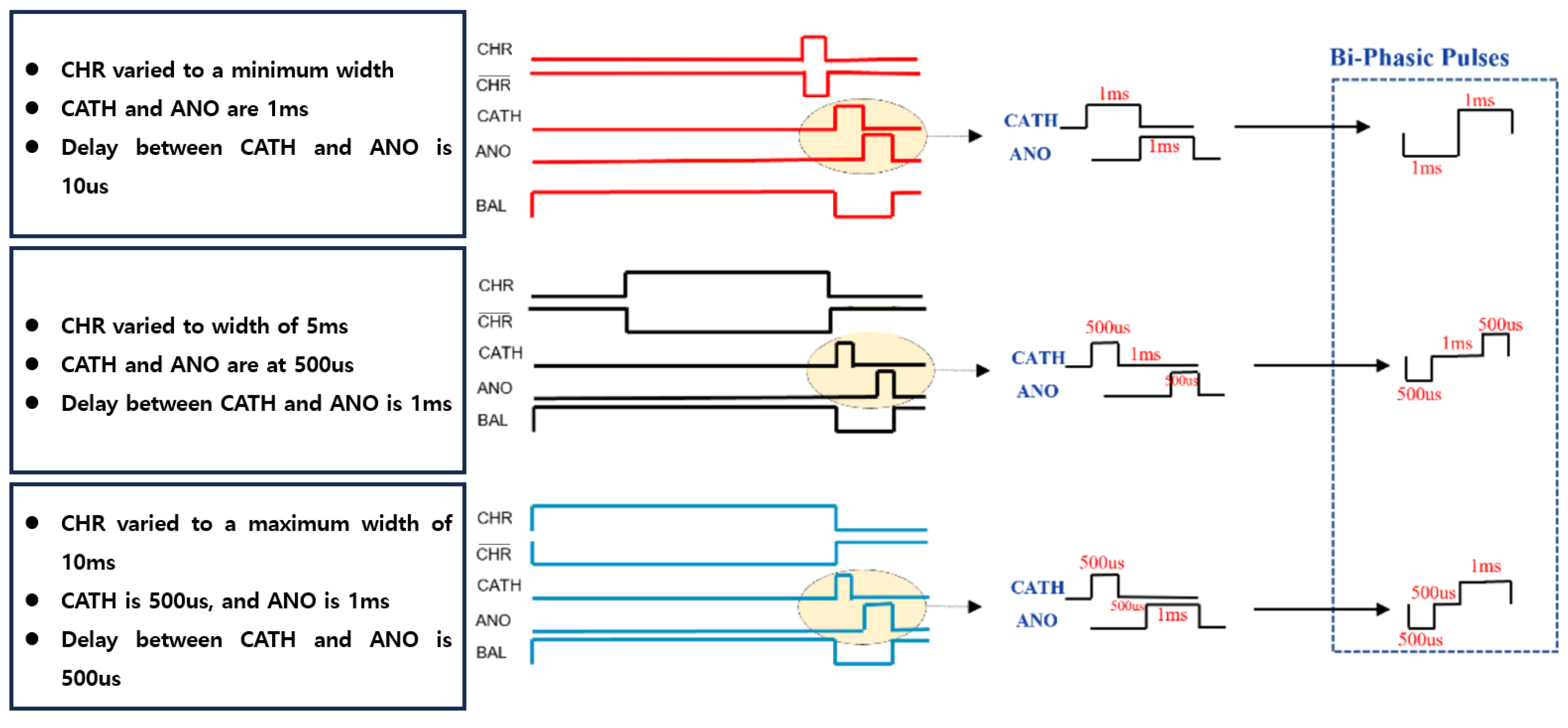
Figure 6 presents a detailed representation of the various pulse shapes and amplitudes derived from the data. CHR pulses can be modulated between 1 ms and 10 ms. CATH and ANO, which combine to form cathodic and anodic shapes of biphasic pulses, are generated in 128 different shapes and amplitudes. This feature provides our system with multiple options for controlling current leakage and crosstalk between the electrodes. Furthermore, these options enable the adjustment of stimulation current according to the different stimulation threshold values of individual patients. Another characteristic of this stimulation approach is the generation of overlapping ANO and CATH pulses. This technique effectively reduces the total stimulation time. Furthermore, creating two overlapping pulses with a 500 µs time interval further minimizes current leakage.
3. Results
3.1. Integrated Circuit Design
To validate the synthesized logic, a Design Vision e-2013 was employed to create the Verilog gate level code and design the layout. An integrated circuit chip that will be implanted inside the eye was created using a 0.18 μm SK Hynix CMOS standardized procedure, which minimized the size and external connections.
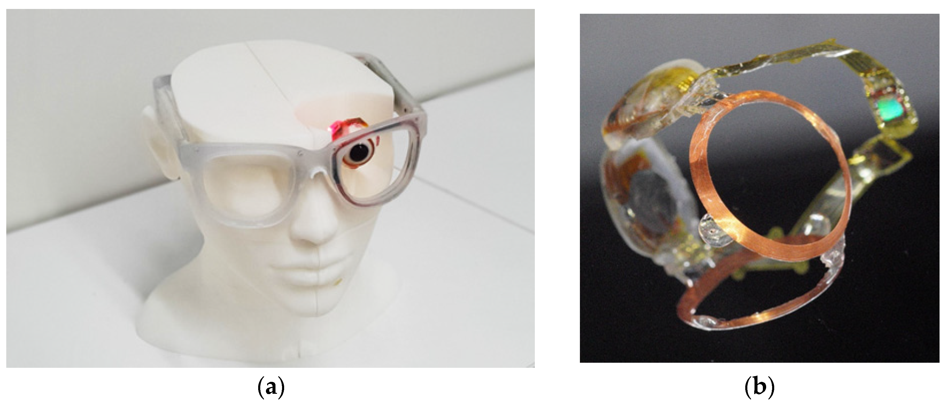
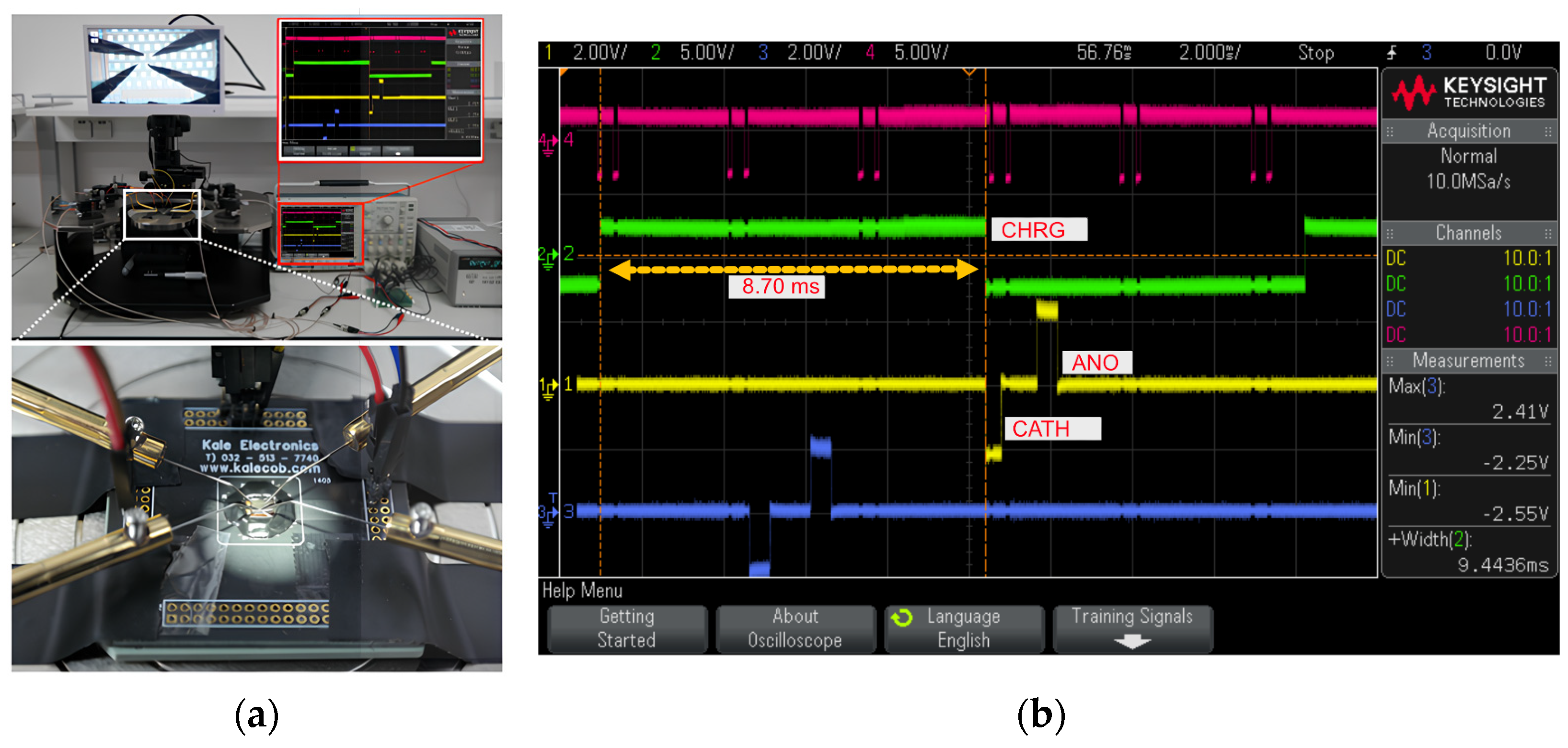
Figure 7 shows a representation of the complete system implemented on a non-biological eye model and the chip utilization. The non-biological eye model was used to test the feasibility of wireless power and data transmission. The LEDs illuminated in
Figure 7a indicate that wirelessly transmitted power and data signals from the transmitter are being received successfully, as described in 2.2.3. The transmitter was designed and implemented on a single PCB, which included a complete wireless transmission system, and the digital controller was implemented on a smaller FPGA (CMOD A7, Xilinx, San Jose, CA, USA) to achieve a compact system. The receiver and stimulator were interconnected to deliver the data, and an enlarged image of the integrated system is shown in
Figure 7b.
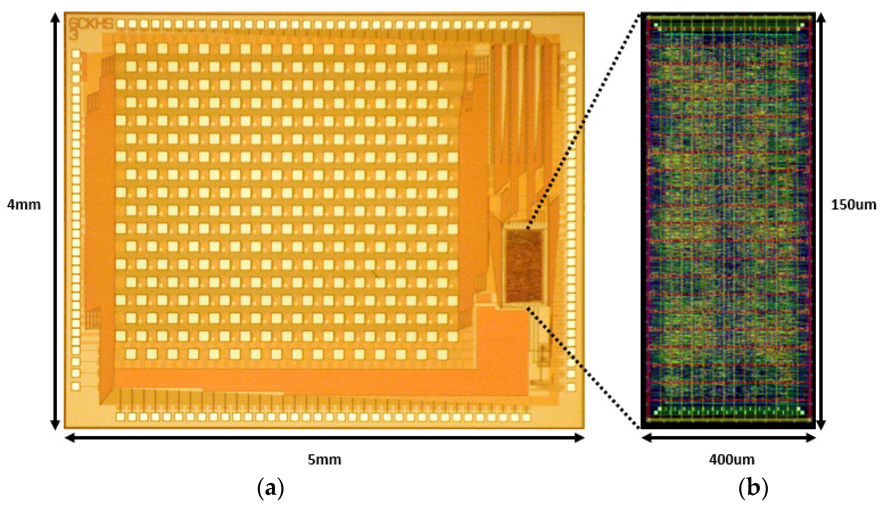
Figure 8 shows the entire layout of the digital controller. A digital controller was fabricated along with a stimulator on a single chip following a 0.18 μm SK Hynix CMOS standard process.
Table 1 provides the performance of the 256-pixel chips. The combination of overlapping pulse techniques and precise control over biphasic pulses enabled effective current management, while a voltage range of −2.5 V to 2.5 V was applied across the system to minimize crosstalk and current leakage during stimulation.
3.2. ModelSim Simulations
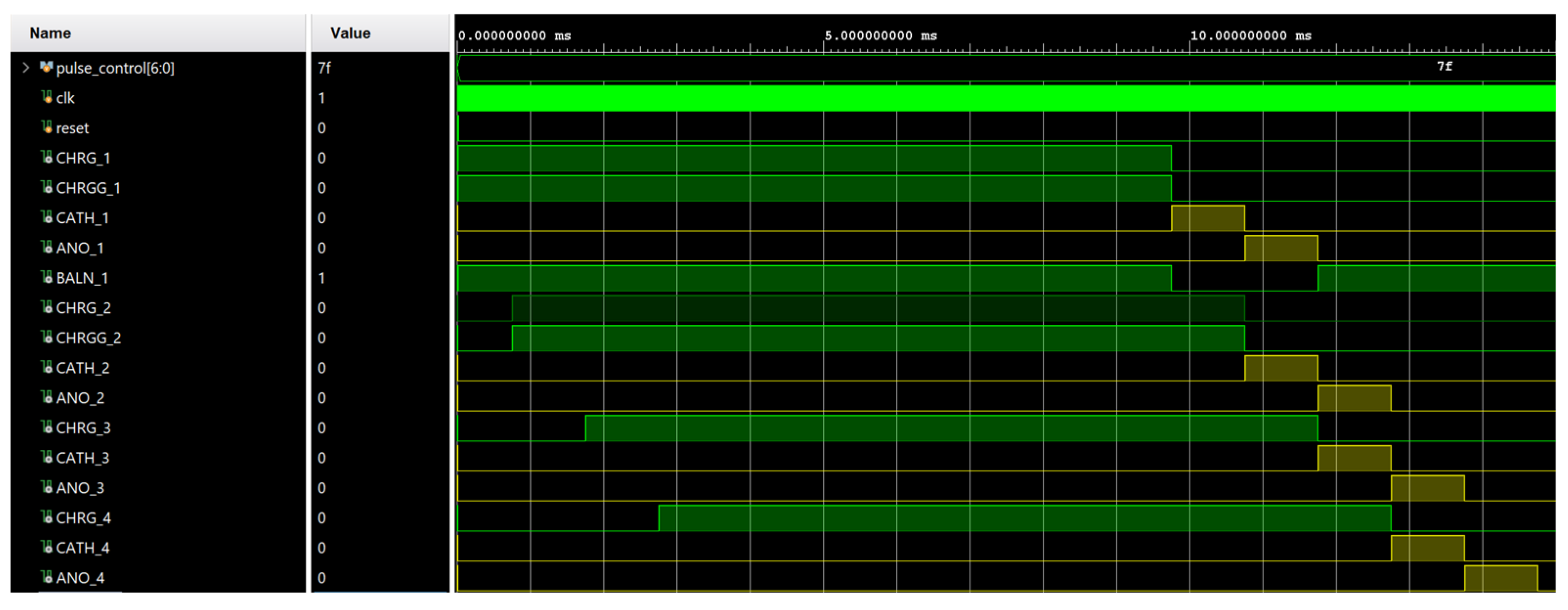
Vivado version 2020.1 was used for the simulations of the 256-pixel digital controller. The concept of overlapping current pulses was simulated, as shown in
Figure 9. Overlapping pulses not only reduced the total stimulation time but also helped to reduce the current leakage that might occur while shifting from the stimulation of a phase to the next phase.
3.3. Microchip Implementation
To verify the accurate operation of the digital controller, a transmitter was developed using an FPGA (CMOD A7, Xilinx, San Jose, CA, USA) for data transmission. The digital controller processes signals received from the FPGA and generates various pulse patterns. The CHR pulse length was calculated with respect to the received data. The different shapes of the biphasic pulse based on CATH and ANO are shown in
Figure 10. In this figure, the biphasic pulse is generated on the specific datum “11111110”, which generates CHR and
pulses for 8.70 ms. For every specific datum, a varied pulse width is generated. The different amplitude and shape of the biphasic pulse are generated based on these data. The input 8-bit data contained in a 32-bit data packet enabled our system to generate 128 different widths and shapes of biphasic pulses. Varying shapes and amplitudes based on incoming light give our system full control over the current.
4. Discussion
This study presents a novel wireless digital controller for high-density stimulation devices. The proposed system addresses key challenges in retinal prostheses, including resolution enhancement, crosstalk reduction, and flicker-free vision. By integrating a hexagonal electrode structure and an overlapping stimulation technique, the system effectively mitigates the drawbacks of high-density electrode arrays while maintaining low power consumption.
One of the key challenges in high-density retinal implants is electrical crosstalk, which can reduce spatial resolution and lead to distorted visual perception [
20]. Our system addresses this issue by placing the reference electrode near the active electrodes, thereby limiting the spread of charge and preventing unwanted activation. This spatial optimization is essential in high-resolution retinal prostheses, as previous studies have shown that higher electrode densities improve visual acuity and increase crosstalk risks [
25]. By incorporating a hexagonal stimulation pattern, our digital controller effectively controls the stimulation area.
Power efficiency is critical in retinal implants, as excessive power consumption can lead to heat dissipation and potential tissue damage [
17]. Our system consumes 3.2 mW, slightly higher than some previous designs but necessary to support the 256 independent stimulation channels. The overlapping stimulation technique balances this trade-off, which ensures a flicker-free vision frequency, enhancing patient comfort [
26]. Future work should focus on optimizing power management strategies to reduce energy consumption further while maintaining high-resolution stimulation.
Another key contribution of our study is the global digital controller, which enables dynamic pulse shaping with 128 distinct biphasic pulse patterns, allowing patient-specific stimulation adjustments. Tailoring stimulation parameters is essential for minimizing current leakage and preventing overstimulation [
7,
8]. While our system demonstrated stable performance, further improvements in stimulation algorithms could enhance spatial resolution and long-term efficacy, ensuring its clinical viability.
Despite these advancements, this study has limitations that should be addressed in future research. While the system was validated through simulations and prototype testing, further biological validation using animal models or clinical trials is necessary to assess its safety and efficacy in real physiological environments. Additionally, although the hexagonal stimulation pattern effectively reduces crosstalk, further refinement of stimulation algorithms could enhance spatial resolution. Future research should explore higher-density electrode arrays, machine learning-based adaptive stimulation, and long-term clinical trials to ensure the system’s real-world viability. By integrating optimized pulse shaping, efficient wireless telemetry, and a compact digital architecture, our system represents a clinically promising advancement in high-density retinal prostheses, offering a potential breakthrough for patients with retinal degenerative diseases.
5. Conclusions
This study presents a 256-pixel retinal prosthesis system featuring a digital controller capable of dynamic biphasic pulse generation for high-density, low-crosstalk stimulation. The proposed design demonstrates several significant advancements over existing technologies, addressing key challenges in retinal prosthesis development, including current leakage, crosstalk, and power efficiency. Additionally, this study proposes a solution for implementing low-sensitivity electrodes while addressing flicker-free vision through an overlapping current pulse technique. The overlapping technique, with minimal time delay, enables precise control over current loss.
Moreover, generating 128 distinct pulse shapes and amplitudes allows for adaptive stimulation tailored to individual light intensities and patient-specific retinal thresholds. This feature enhances the versatility of the system and demonstrates its potential to be deployed in a wide range of clinical applications. Additionally, the integration of wireless telemetry for power and data transmission ensures that the device remains compact and suitable for implantation.
The performance of the system was validated through hardware implementation, simulation, and oscilloscope testing. The fabricated chip, based on a 0.18 μm CMOS process, demonstrated reliable functionality with a compact active area and minimal external connections. The results of this study indicate that the proposed system has the potential to be a commercially viable device, as evidenced by various tests that meet general safety requirements.
In the future, we aim to develop a more advanced system by enhancing control over flicker-free vision and crosstalk while increasing the resolution of the system. Future research will implement a chip with a resolution beyond 2000 pixels and integrate refined control algorithms.
