Article

A 328 nW, 0.45 V Current Differencing Transconductance Amplifier and Its Application in a Current-Mode Universal Filter

1
Department of Microelectronics, Brno University of Technology, Technická 10, 601 90 Brno, Czech Republic
2
Department of Electrical Engineering, Brno University of Defence, Kounicova 65, 662 10 Brno, Czech Republic
3
Department of Telecommunications Engineering, School of Engineering, King Mongkut’s Institute of Technology Ladkrabang, Bangkok 10520, Thailand
4
Department of Electrical Engineering, Czestochowa University of Technology, 42-201 Czestochowa, Poland
*
Author to whom correspondence should be addressed.
Appl. Sci. 2025, 15(7), 3471; https://doi.org/10.3390/app15073471
Submission received: 11 February 2025 / Revised: 13 March 2025 / Accepted: 19 March 2025 / Published: 21 March 2025

Abstract

:
This paper presents a low-voltage, low-power current differencing transconductance amplifier (CDTA) utilizing the bulk-driven MOS transistor technique in the subthreshold region for reduced voltage and power consumption. The proposed CDTA includes a z-copy terminal, which enhances its functionality in current-mode circuit applications. Designed in the Cadence Virtuoso environment using 0.18 µm CMOS technology from Taiwan Semiconductor Manufacturing Company (TSMC), the amplifier operates with a supply voltage of 0.45 V and consumes 328 nW of power, with a bias current set to 10 nA. The current bandwidth and offset of the CDTA are 35 kHz and 0.3 nA, respectively. To demonstrate its performance, the CDTA is applied in a current-mode universal filter, which can realize low-pass, band-pass, high-pass, band-stop, and all-pass responses within a single topology. This design eliminates issues related to inverting input signals, input signal matching, or the need for multiple input signals. Additionally, the natural frequency of these filtering functions can be electronically controlled. The low-pass filter achieves a dynamic range of 61 dB, with a total harmonic distortion of 0.8%.

1. Introduction

The current differencing transconductance amplifier (CDTA) is an active building block for current-mode signal processing applications [1,2]. It is widely used in various applications, including universal filters [2,3,4,5,6], sinusoidal oscillators [7,8,9], capacitance multipliers [10,11], precision rectifiers [12,13], memristor emulators [14,15,16], and chaotic oscillators [17]. However, traditional CDTA circuits are not suitable for low-voltage, low-power applications because their design does not inherently support efficient operation under these conditions. In modern electronic systems, both analog and digital circuits increasingly require low-voltage, low-power operation [18,19,20].
Several low-voltage, low-power CDTAs have been reported in the literature [21,22,23,24,25]. The circuit in [21] operates with a ±0.6 V supply voltage and consumes 143 μW of power using 0.18 µm TSMC technology. In [22], a ±1.4 V supply voltage is used, with a power consumption of 2.6 mW using 130 nm TSMC technology. The circuit in [23] operates with a ±0.8 V supply voltage and demonstrates low power consumption using 0.18 µm CMOS technology. Another design in [24] uses a ±1 V supply voltage and consumes 0.1 mW of power using 0.18 µm CMOS technology, while [25] operates with a 0.5 V supply voltage and consumes 1.05 μW using 0.18 µm CMOS technology.
Universal filters provide five fundamental filtering functions, low-pass filter (LPF), high-pass filter (HPF), band-pass filter (BPF), band-stop filter (BSF), and all-pass filter (APF), within a single topology. These filters are extensively used in communication, control, electronics, and instrumentation systems. For example, they are employed in crossover networks for high-fidelity loudspeakers and for tone decoding in touch-tone telephones [26,27]. Low-voltage, low-power universal filters are becoming increasingly important in biomedical systems [28]. In current-mode signal processing circuits, they offer several advantages, such as wide signal bandwidth and ease in adding and subtracting current signals. The ideal characteristics of current-mode filters include low input and high output impedance, no requirement for input signal matching, and no need for inverted input signals, thereby eliminating the need for additional circuitry. Several low-voltage, low-power current-mode universal filters have been proposed using various active devices, such as transconductance amplifiers [29,30,31] and voltage second-generation current conveyors (VCII) [32,33]. In recent years, reducing the supply voltage and power consumption of active elements has become essential, particularly for wearable and biomedical applications [34,35,36,37].
This paper presents a low-voltage, low-power CDTA that utilizes the bulk-driven MOS transistor technique, operating in the weak inversion region, to achieve its low-voltage and low-power characteristics. To demonstrate the advantages of the proposed CDTA, it is applied in current-mode universal filters. The proposed filter provides both non-inverting and inverting transfer functions for LPF, HPF, BPF, BSF, and APF, with low input and high output impedances, electronic tuning capability, no component-matching requirements, and no inverted input signals. Additionally, the natural frequency of the filter can be electronically controlled.

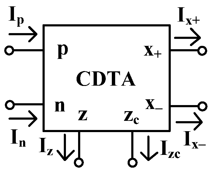
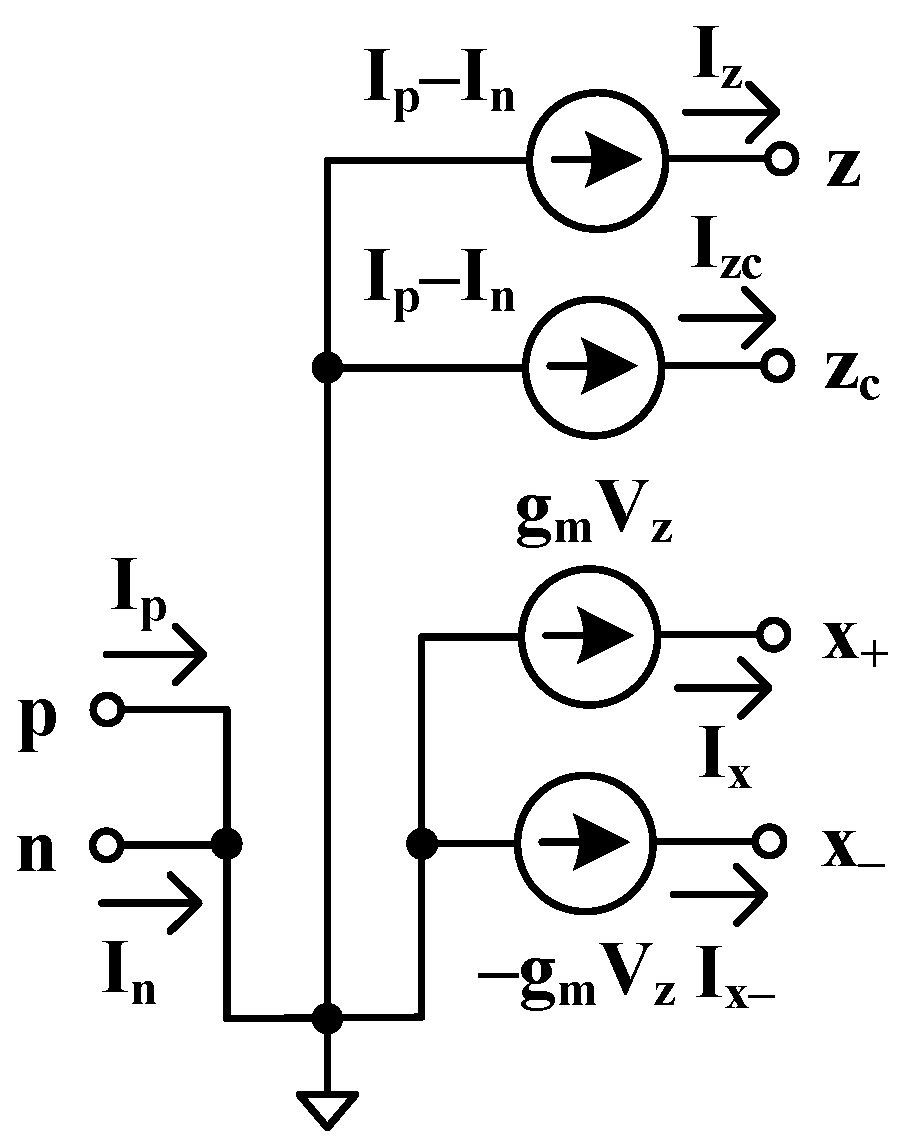
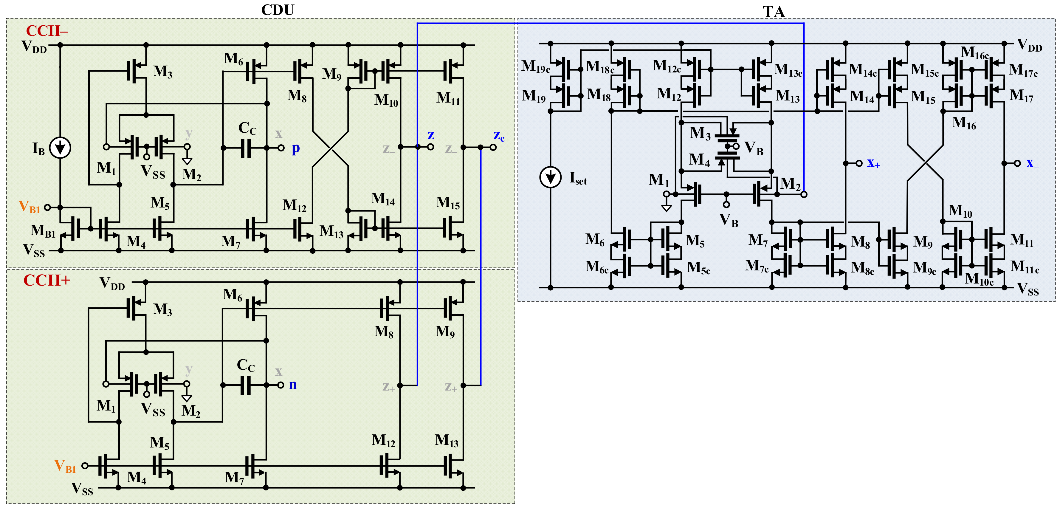
2. Circuit Description

2.1. Proposed 0.45 V CDTA

The electrical symbol of the CDTA is shown in Figure 1, and its equivalent circuit is illustrated in Figure 2. The ideal characteristics of the CDTA can be described as follows:
V p = V n = 0 I z = I z c = I p I n I x ± = g m V z
where g m is the transconductance gain, I p and I n are the input currents, and I z , I z c , and I x are the output currents of the CDTA. The zc-terminal of the CDTA is introduced to enhance its functionality in current-mode circuit applications. Therefore, in the design of the CDTA, the p- and n-terminals should ideally exhibit low impedance (ideally zero), while the z-, zc-, and x-terminals should have high impedance (ideally infinite).
Figure 3 shows the CMOS implementation of the proposed CDTA. The circuit consists of a minus-type current conveyor (CCII−), a plus-type (CCII+), and a transconductance amplifier (TA). Both the CCII− and CCII+ form a current differencing unit (CDU) [21], with their output z connected to the TA. Even though the proposed CDTA is composed of known blocks, it includes a z-copy terminal, which enhances its functionality in current-mode circuits, and this feature is demonstrated in the proposed filter design.
The CCII+ functions as a current follower ( I n = I z + ), while the CCII− functions as an inverted current follower ( I p = I z ). Since the outputs of the CCII+ and CCII− are connected at the z- terminal, the function of the CDU is realized, such that ( I z = I p I n ) . The zc-terminal of the CDTA is implemented using complementary current mirrors.
The z-terminal of the CDU is connected to the non-inverting terminal of the TA, while the inverting terminal is grounded. When the z-terminal is loaded with an impedance, the current I z is converted into a voltage V z . This voltage is then converted into a current I x at the x-terminal of the TA. Consequently, the ideal characteristic I x = g m V z of the CDTA is achieved.
The MOS differential pairs of the CCIIs are implemented using bulk-driven MOS transistors (M1 and M2). These differential pairs are loaded by transistors M4 and M5 and supplied by transistor M3. This configuration is based on the flipped voltage follower (M1–M5), which enables operation with a minimal supply voltage. Consequently, the proposed CCII achieves a reduced minimum supply voltage, given by the sum of the source-gate voltage of M3 and the drain-source voltage of M4, as follows:
V D D ( m i n ) = V S G M 3 + V D S ( s a t ) M 4
where V S G M 3 is equal to at least V D S ( s a t ) M 3 + V D S ( s a t ) M 1 . For circuit stability, Miller frequency compensation is applied using the capacitance CC.
Assuming unity-gain current mirrors in the current conveyors, with identical transistors (M6 = M8 = M9–M11 and M7 = M12–M15), the input resistance at the p-terminal ( r p ), the input resistance at the n-terminal ( r n ), and the output resistance at the x-terminal of the CDTA can be expressed, respectively, by
r p = r n = 1 g m 6 g m b 1 , 2 r d s 2 r d s 5
r z 1 2 g d s 8 , 10 +   g d s 12 , 14
r z c 1 2 g d s 9 , 11 + g d s 13 , 15
r x = r d s 8 1 + g m 8 r d s 8 c | |   r d s 14 1 + g m 14 r d s 14 c
where g m j , g m b j , and r d s j are, respectively, the gate transconductance, bulk transconductance, and output resistance of the j th MOS transistors. It should be noted that the input resistances r p and r n of this CDTA structure are equal, since CCII− and CCII+ are identical.
The input-referred thermal noise of the differential amplifier is used to determine the input noise of the proposed CDTA, which can be expressed by
v ¯ n 2 2 8 k T 3 g m b 1 2 g m 1 , 2 + g m 4 , 5
k is the Boltzmann constant ( ~ 1.38 × 10⁻²³ J/K), and T is the absolute temperature.
The TA of the CDTA is composed of a bulk-driven (BD) linearized differential pair and current mirrors. To achieve high output resistance and, consequently, improve the DC voltage gain, self-cascode current mirrors are utilized. The linearity of the input pair is enhanced through the use of BD transistors M3 and M4, which operate in the triode region [38]. The biasing current, I s e t , is employed to adjust the transconductance g m . Assuming unity-gain current mirrors, the DC transfer characteristic of the TA in the subthreshold region is given by
I x = 2 I s e t t a n h η V z 2 n p U T t a n h 1 1 4 m + 1 t a n h η V z 2 n p U T
where η = g m b / g m is the bulk-to-gate transconductance ratio, n p is the subthreshold slope factor, U T is the thermal potential, and m = (W/L3,4)/(W/L1,2) should be equal to 0.5 for optimal linearity in the weak inversion region [38]. The small-signal transconductance of the OTA is expressed as follows:
g m = η · 4 m 4 m + 1 · I s e t n p U T
The DC voltage gain is
A v T A     g m g m 8 r d s 8 r d s 8 c | | g m 14 r d s 14 r d s 14 c
Thus, the voltage gain is increased by employing self-cascode connections, which enhance the output resistance of the TA stage.
The circuit was designed as follows. The bias currents in the whole structure determine its power dissipation and should be chosen as low as possible. However, their minimum values in the input stage of the CCII are limited by thermal noise, which is a dominant source of noise in the proposed design. Taking into account (7), IB was set to 50 nA, which provides the required level of noise. The biasing currents in all other branches were also set to IB, which entailed g m 6 / g m 1 = 1 and unity-gain current mirrors in the structure. This resulted in g m 6 / g m b 1 equal to about 3 at the operating point, which resulted in a moderate Miller compensation capacitor Cc. The W/L ratios of the transistors in the input stage were chosen to obtain VDS = (VDD − VSS)/3 for each transistor in this stage at the operating point for the assumed biasing currents. For VDD = 0.45 V, this means that VSG3 = 0.3 V and VGS1,2 = 0.3 V if the gate terminals of M1 and M2 are connected to the lowest potential, which is advantageous to decrease the bulk currents and W/L ratios of the input transistors. For the diode-connected p- and n-channel transistors in the current mirrors, |VGS| were chosen to be equal to about mid supply. Such a choice gives a maximum voltage headroom for possible PVT variations and signal swing.
The biasing currents for the transconductance amplifier were chosen to obtain the required value of its transconductance (see (9)). The coefficient m = (W/L3,4)/(W/L1,2) was chosen to be equal to 0.5 for optimal linearity. As previously, in the input stage the voltage drops across the main elements (biasing sources M12,12c and M13,13c and cascode current mirrors M6,6c and M7,7c), and the VDS of the input transistors M1 and M2 were equal to around (VDD − VSS)/3 for nominal biasing currents to maximize voltage headroom for possible PVT variation, transconductance tuning, and signal swing. Regarding the self-cascode connections, the VDS of the most bottom transistors (most upper transistors) operating in the triode region were chosen to be around 30 mV for nominal biasing currents. The biasing voltage VB allowed obtaining proper values of the quiescent voltages at the sources of M1 and M2 for nominal biasing currents and moderate W/L ratios of the input transistors.

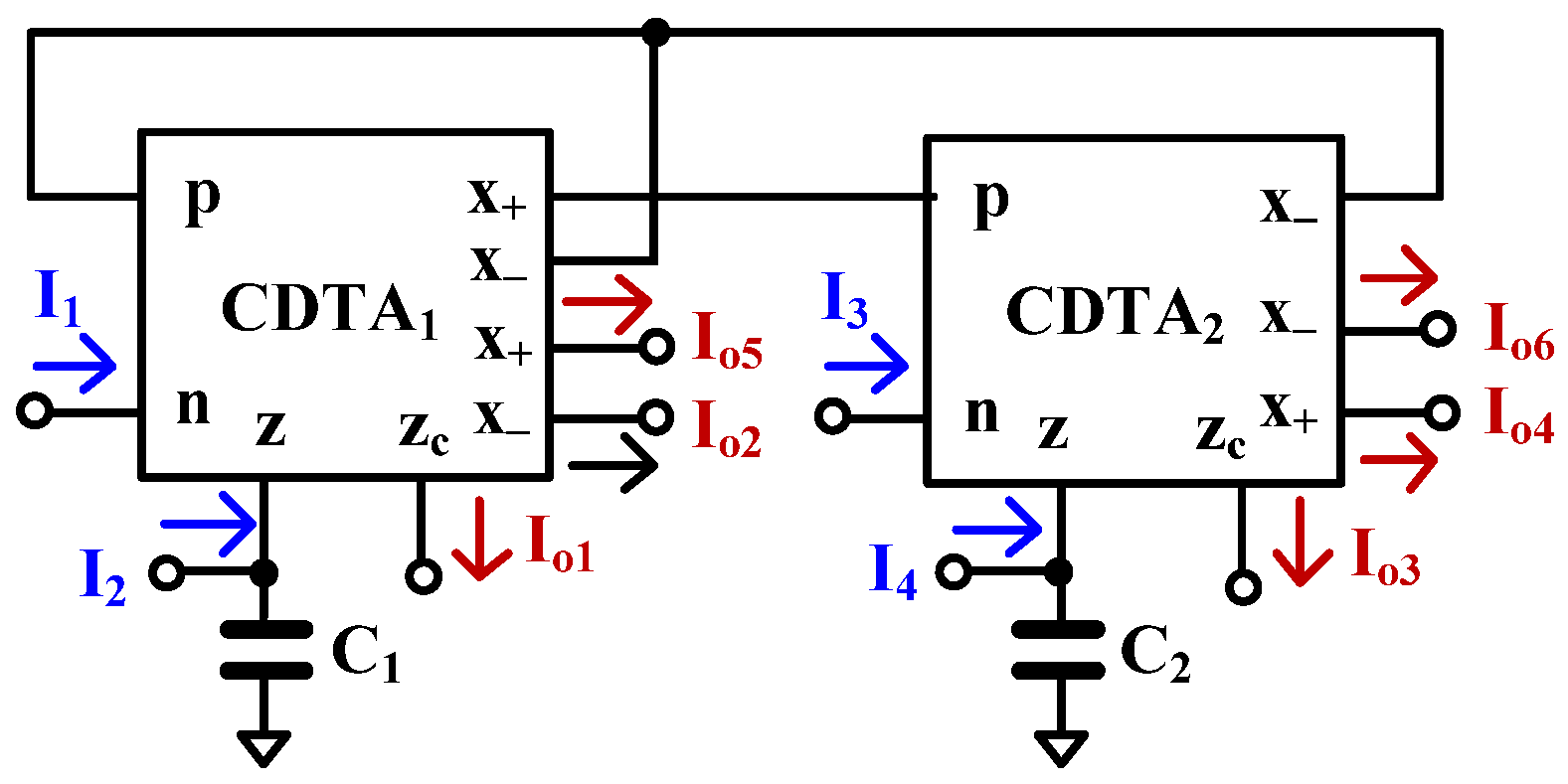
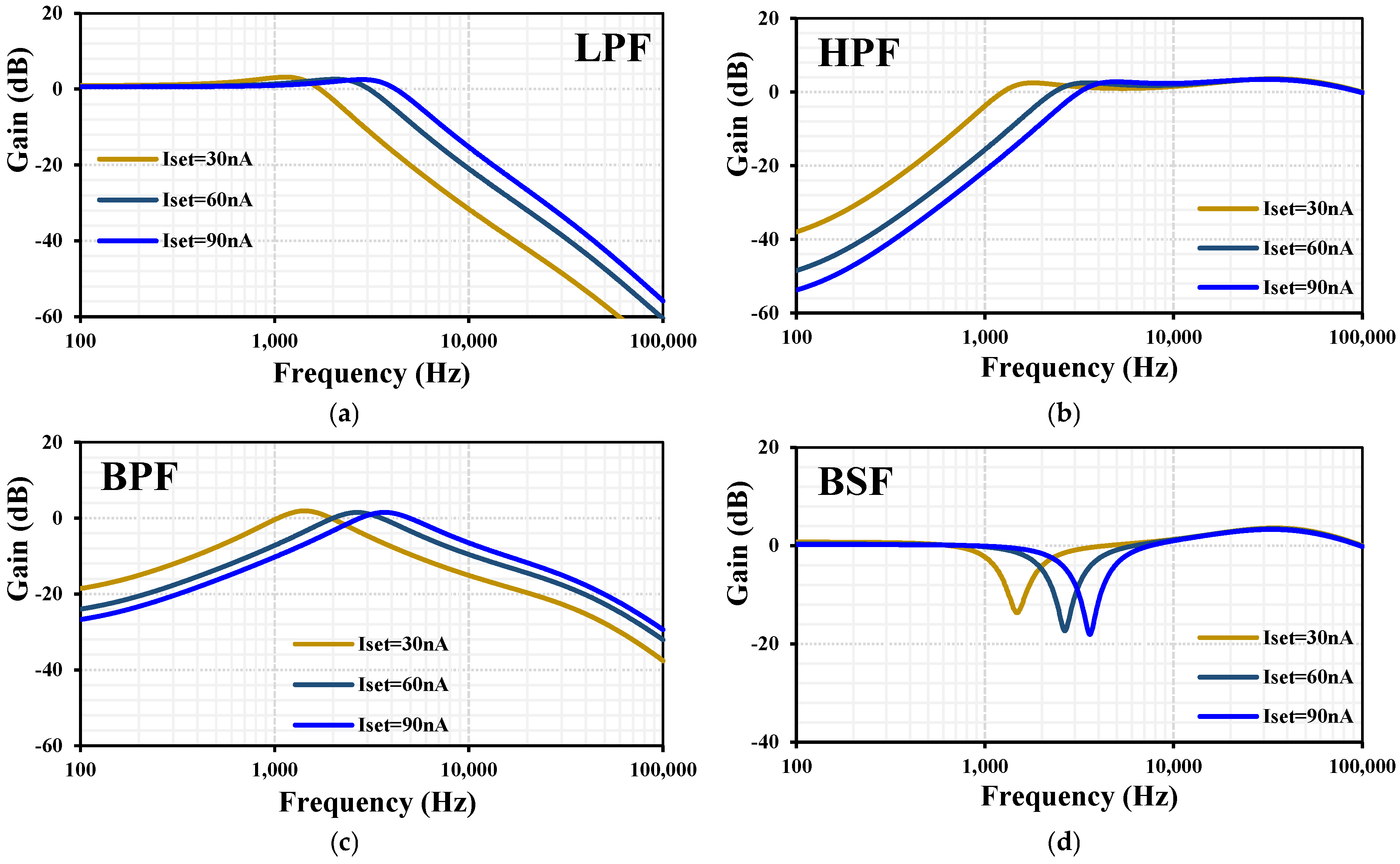
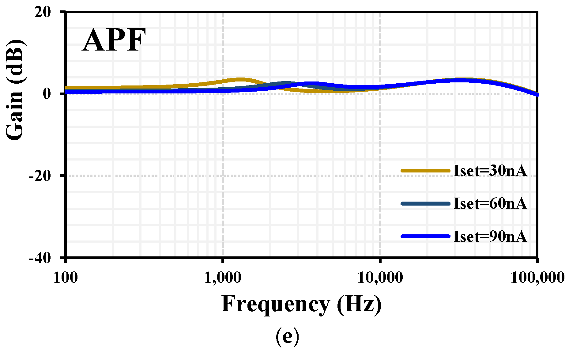
2.2. Proposed Current-Mode Analog Filter

The proposed current-mode analog filter, implemented using CDTAs, is shown in Figure 4. The circuit comprises two CDTAs and two grounded capacitors. The inclusion of grounded capacitors simplifies the compensation of parasitic passive components in the circuit.
When I 1 to I 4 serve as the input terminals and I o 1 to I o 6 as the output terminals, the current outputs of Figure 4 can be derived using the CDTA characteristics given in Equation (1) and nodal analysis as follows:
I o 1 = s 2 C 1 C 2 I 1 s C 2 g m 1 + g m 1 g m 2 I 2 s C 1 g m 2 I 3 s C 1 g m 2 I 4 s 2 C 1 C 2 + s C 2 g m 1 + g m 1 g m 2
I o 2 = s C 2 g m 1 I 1 + s C 2 g m 1 I 2 g m 1 g m 2 I 3 g m 1 g m 2 I 4 s 2 C 1 C 2 + s C 2 g m 1 + g m 1 g m 2
I o 3 = s C 2 g m 1 I 1 + s C 2 g m 1 I 2 + s 2 C 1 C 2 I 1 + s C 2 g m 2 I 3 g m 1 g m 2 I 4 s 2 C 1 C 2 + s C 2 g m 1 + g m 1 g m 2
I o 4 = g m 1 g m 2 I 1 g m 1 g m 2 I 2 s C 1 g m 2 + g m 1 g m 2 I 3 s C 1 g m 2 + g m 1 g m 2 I 4 s 2 C 1 C 2 + s C 2 g m 1 + g m 1 g m 2
I o 5 = s C 2 g m 1 I 1 s C 2 g m 1 I 2 + g m 1 g m 2 I 3 + g m 1 g m 2 I 4 s 2 C 1 C 2 + s C 2 g m 1 + g m 1 g m 2
I o 6 = g m 1 g m 2 I 1 + g m 1 g m 2 I 2 + s C 1 g m 2 + g m 1 g m 2 I 3 + s C 1 g m 2 + g m 1 g m 2 I 4 s 2 C 1 C 2 + s C 2 g m 1 + g m 1 g m 2
Here, g m 1 and g m 2 refer to the transconductance of the first and second CDTA blocks employed in the proposed filter architecture.
Table 1 demonstrates that five standard filtering functions, LPF, HPF, BPF, BSF, and APF, can be realized using a single topology, providing a total of 19 transfer functions. These filtering functions are achieved with a single input signal, eliminating the need for multiple input signals that would require additional components, such as a multiple-input current mirror. Furthermore, the output signals can be directly connected without the need for buffer circuits. As a result, the proposed current-mode analog filter can efficiently realize all five standard filtering functions without requiring any extra circuitry. To implement these filtering functions, inverting-type input signals are not required, thereby eliminating the need for additional inverting current amplifiers. The output terminals I o 1 , I o 2 , I o 3 , I o 4 , I o 5 , and I o 6 exhibit high impedance, allowing them to be directly connected to the next stage without the need for buffer circuits.
The parameters ω o and Q can be expressed, respectively, as follows:
ω o = g m 1 g m 2 C 1 C 2
Q = g m 2 C 1 g m 1 C 2
It is evident from Equations (17) and (18) that the parameter ω o can be controlled by adjusting the transconductance g m (where g m = g m 1 = g m 2 ), while the parameter Q can be adjusted by the ratio C 1 / C 2 .

2.3. Non-Ideal Analysis
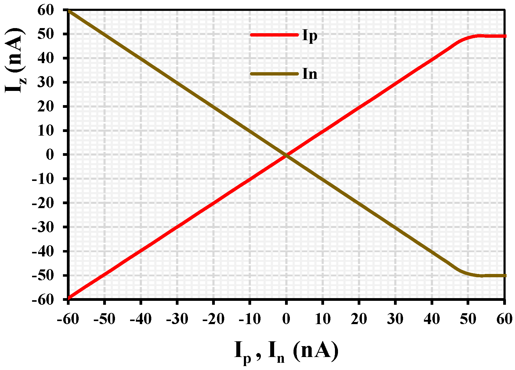
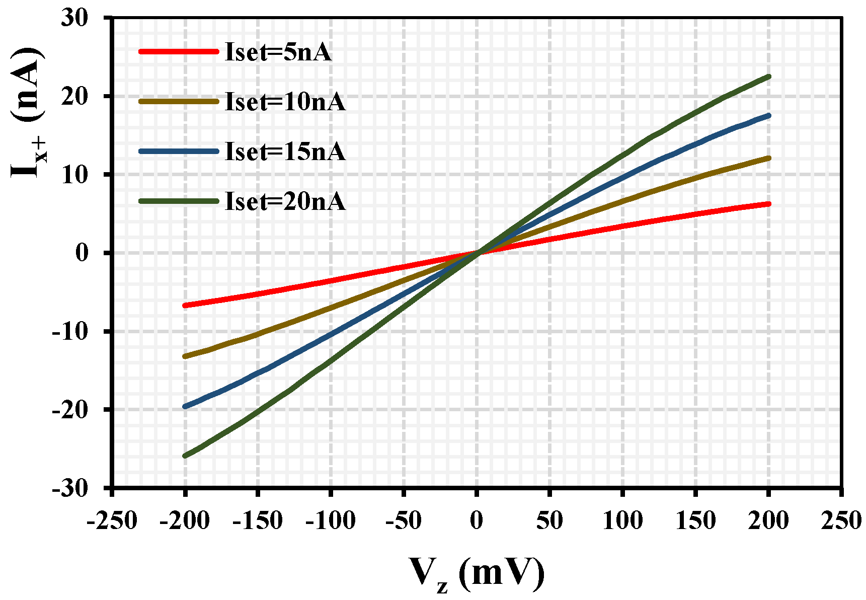
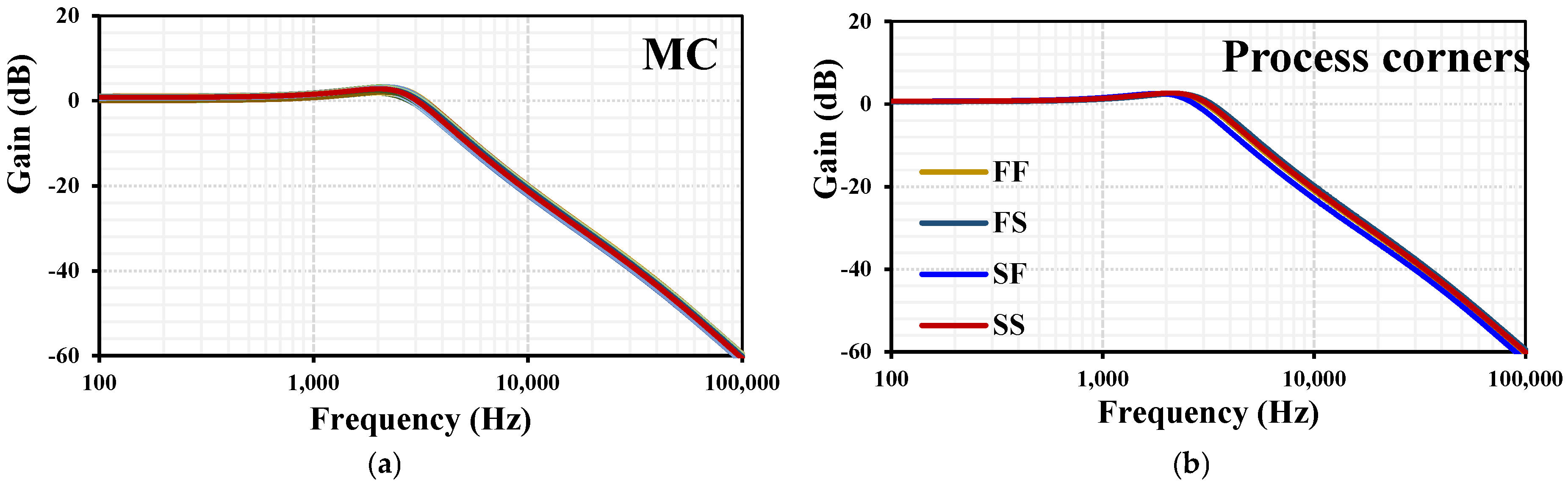
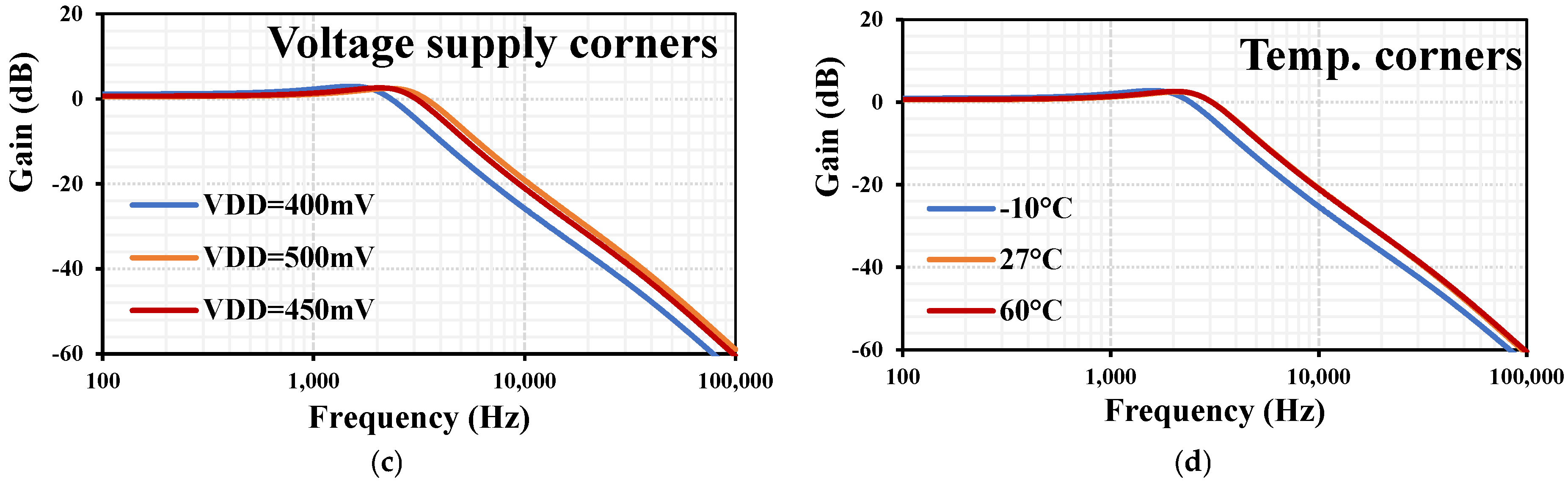
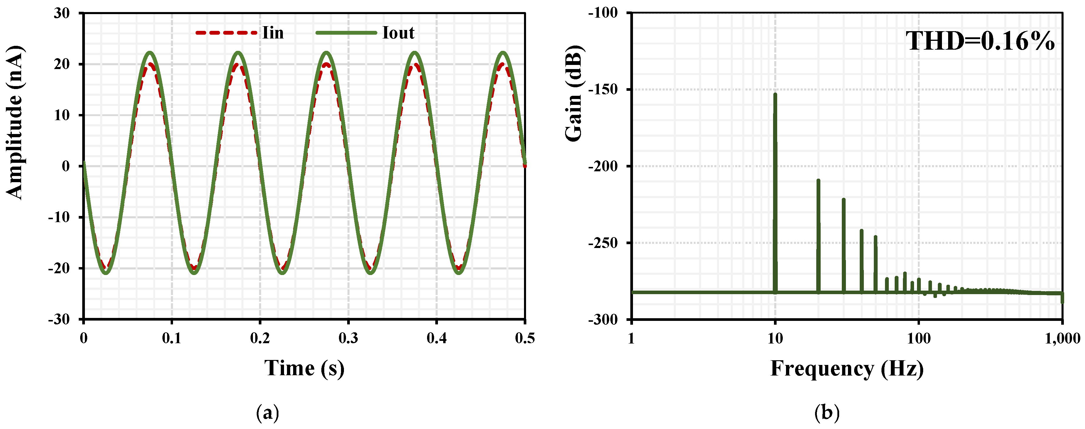
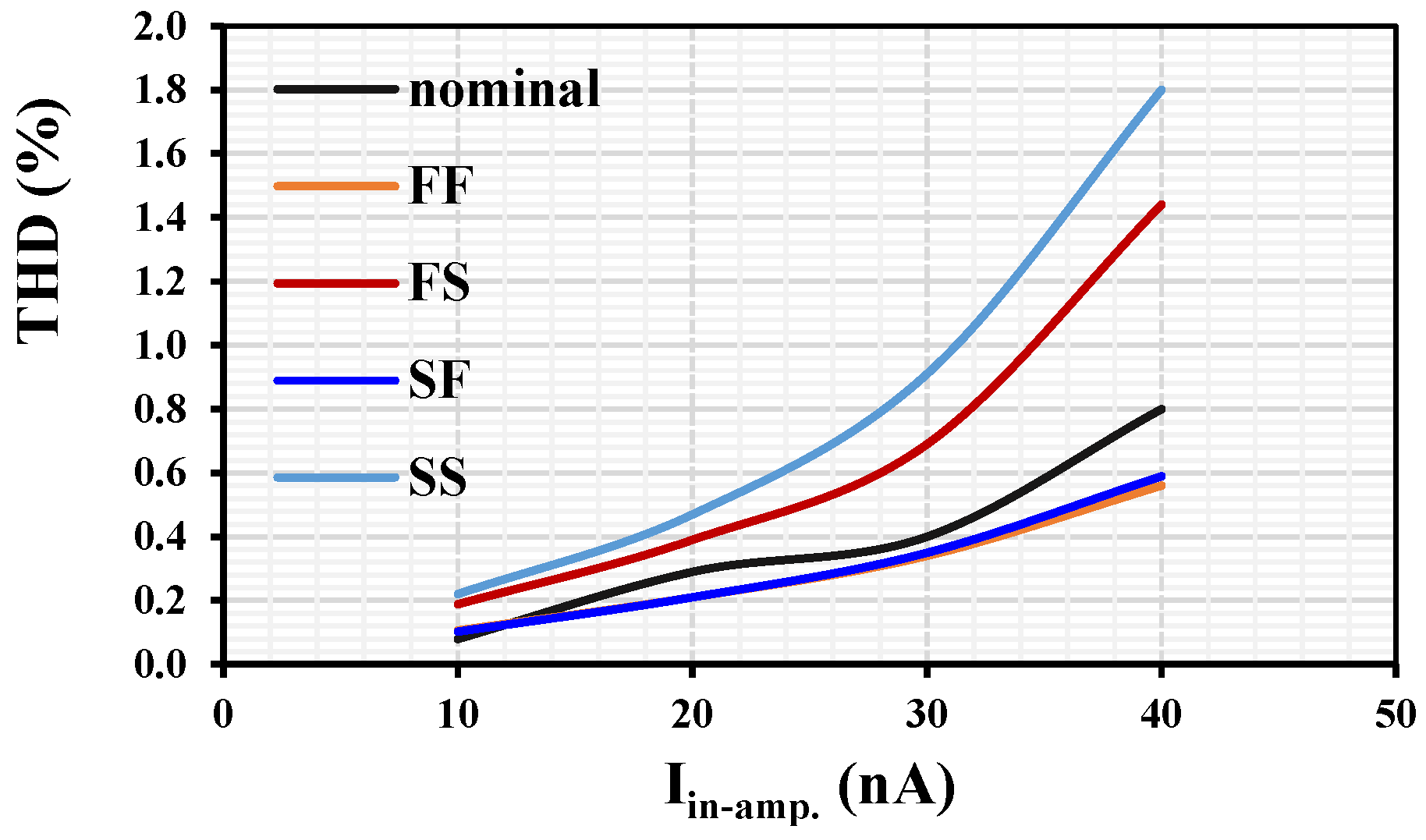
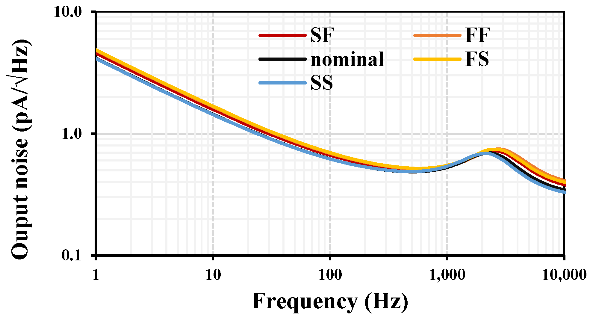
The non-ideal characteristics of the CDTA are taken into account in the analysis of the proposed universal filter. The parasitic current gains between the p- and z-terminals and the n- and z-terminals, along with the non-ideal transconductance, are taken into account. Parasitic impedances are neglected, as the circuit operates at low frequencies typical for biomedical signals. In the non-ideal case, the behavior of the CDTA can be represented, as shown in [2], by the following equation:
V p = V n = 0 I z = α p I p α n I n I x = g m n V z
Here, α p = 1 ε p , where ε p ε p 1 represents the parasitic current gain between the p- and z-terminals of the CDTA. Similarly, α n = 1 ε n , where ε n ε n 1 denotes the parasitic current gain between the n- and z-terminals of the CDTA. Ideally, α p , and α n are all equal to unity. The parameter g m n represents the non-ideal transconductance.
The non-ideal transconductance g m n of the TA at a frequency near its cut-off can be expressed [39] as follows:
g m n s g m 1 s T o
where T o = 1 / ω g m and ω g m represents the first pole frequency of g m .
Using (19) and nodal analysis, the denominator of the transfer functions can be rewritten as follows:
D s = s 2 C 1 C 2 + s C 2 g m 1 α p 1 + g m 1 g m 2 α p 1 α n 2
where α p j , and α n j are the parasitic current gains of the j th CDTA.
Considering the non-idealities in (20) for g m 1 and g m 2 , the non-idealities can be approximated as g m n 1 s g m 1 1 s T o 1 and g m n 2 s g m 2 1 s T o 2 . The denominator D s of the transfer functions of the filters can be then written as follows:
D s = s 2 C 1 C 2 1 C 2 g m 1 α p 1 T o 1 g m 1 g m 2 α p 1 α n 2 T o 1 T o 2 C 1 C 2                                                                                                         + s C 2 g m 1 α p 1 1 g m 1 g m 2 α n 2 T o 1 + T o 2 C 2 g m 1 + g m 1 g m 2 α p 1 α n 2
From (22), the non-ideal effects of the transconductances g m 1 and g m 2 can be mitigated by satisfying the following conditions:
C 2 g m 1 α p 1 T o 1 g m 1 g m 2 α p 1 α n 2 T o 1 T o 2 C 1 C 2 1
g m 1 g m 2 α n 2 T o 1 + T o 2 C 2 g m 1 1
These conditions can be achieved by appropriately selecting the values of g m 1 and g m 2 and capacitances C 1 and C 2 .
In the non-ideal case, the natural frequency and quality factor of the proposed filter become
ω o = g m 1 g m 2 α p 1 α n 2 C 1 C 2
Q = g m 2 C 1 α n 2 g m 1 C 2 α p 1

3. Results

The simulation results were generated using the Cadence Virtuoso program using 0.18 µm CMOS technology from TSMC. The transistor aspect ratio of the CMOS structure of the CDTA is shown in Table 2. The bias current for the CCII ( I B ) was 50 nA, and the bias voltage for the TA ( V B ) was −50 mV. The voltage supply was 450 mV (±225 mV), and the power consumption of the CDTA shown in Figure 3, with I s e t = 10 nA, was 328 nW.
Figure 5 shows the CDU DC characteristics of the I z versus I p and I z versus I n of the CDTA for V z   = 0. It is evident that the circuit can process signals up to 50 nA, which is equal to the bias current of the CCII. Figure 6 demonstrates the TA DC characteristics of the I x + versus V z with various I s e t of the TA. The circuit is capable of processing input voltages in the range of ±200 mV while the voltage supply is ±225 mV, confirming the circuit’s ability to operate under low supply voltages. The overall performance of the proposed CDTA is summarized in Table 3. Compared with the previous CDTAs in [21,22,23,24,25], the proposed structure provides a low supply voltage and low power consumption.
For the filter application in Figure 4, the capacitance values were chosen as C 1 = C 2 = 20 pF. With I s e t = 60 nA, the frequency response of the filter is shown in Figure 7, where the simulated cut-off frequency was 2.66 kHz, the quality factor was 1, and the power consumption of the filter was 1.098 µW.
Figure 8 demonstrates the electronic tuning capability of the filter using different values of I s e t = (30, 60, and 90) nA. The corresponding cut-off frequencies were (1.47, 2.66, and 3.58) kHz, respectively.
To confirm the stability and robustness of the filter design, both Monte Carlo (MC) analysis and process, voltage, temperature (PVT) corner analysis were performed. The MC analysis was run with 200 cycles, including process and mismatch variations. Regarding the PVT analysis, the process corners were fast–fast (FF), slow–fast (SF), fast–slow (FS), and slow–slow (SS). The voltage supply corners were selected at 400 mV and 500 mV, and the temperature corners were −10 °C and 60 °C. As shown in Figure 9, the curves overlap in the case of MC and process corners, confirming the proper design of the MOS structure. The variation in the voltage corner at 400 mV results in a reduced bias current and cut-off frequency. In the case of temperature variations, the slight deviation in the cut-off frequency at −10 °C is expected due to the sensitivity of the MOS transistor operating in the subthreshold region to temperature. The circuit offers advantages in electronic tunability. As a result, deviations caused by temperature, process variations, and voltage supply corners can be easily compensated by adjusting the filter’s setting current, allowing for the readjustment of the required cut-off frequency.
Figure 10a shows the transient response of the LPF when a sine wave input signal with an amplitude of 20 pA at 10 Hz is applied to the filter input, with I s e t = 60 nA. The output signal spectrum with total harmonic distortion (THD) shown in Figure 10b confirms a low distortion of 0.16% in the output signal.
Figure 11 shows the THD with various corners versus the amplitude of the input signal at 10 Hz. The nominal THD is less than 0.8% for a 40 nA amplitude of the input signal, confirming the low THD of the proposed filter. The equivalent output current noise of the LPF with various corners is shown in Figure 12. The integrated noise in the filter band from 1 to 2.66 kHz was 42.35 pA, resulting in dynamic range (DR) of 61 dB for 0.8% THD.
The proposed current-mode universal filter was compared with previously developed low-voltage universal filters in [25,29,31,32], as shown in Table 4. Compared to these earlier works, the proposed filter provides the most transfer functions among the five standard filtering functions. Unlike the MISO filters in [25,29,31], the proposed filter does not require an input-matching condition (i.e., I i n = I i n 1 = I i n 2 = I i n 3 [29]) or a double-input condition (i.e., I i n = 2 I i n 1 = I i n 2 [31]). The VCII-based filter in [32] lacks electronic tuning capability and suffers from the use of a floating resistor compared to the proposed topology. However, the universal filter in [29] achieves the lowest supply voltage and power consumption, made possible by a specialized technology (32 nm CNTFET). In addition, the filters in [25,31] exhibit better THD and the filter in [25] demonstrates better DR compared to the proposed filter; however, they consume more power.

4. Conclusions

This research presents a low-voltage, low-power CDTA, implemented using the bulk-driven MOS transistor technique to achieve a low supply voltage. The proposed CDTA is applied in a current-mode universal filter to demonstrate its performance. This universal filter can realize transfer functions for low-pass, band-pass, high-pass, band-stop, and all-pass responses within a single topology. All transfer functions are implemented with high output impedance, which is essential for current-mode circuits. The circuit addresses challenges related to inverting input signals, input signal matching, and the need for multiple input signals. Additionally, the natural frequency of the filters can be electronically controlled, providing an easy method to compensate for temperature variations. The CDTA and its application were designed using 0.18 µm CMOS technology.

Author Contributions

Conceptualization, F.K., M.K. and T.K.; methodology, F.K., M.K. and T.K.; software, F.K. and M.K.; validation, F.K. and M.K.; formal analysis, T.K. and M.K.; investigation, F.K., M.K. and T.K.; resources, M.K.; data curation, F.K. and M.K.; writing—original draft preparation, F.K., M.K., T.K. and J.V.; writing—review and editing, F.K., M.K., T.K. and J.V.; visualization, F.K. and M.K.; supervision, F.K. and M.K.; project administration, F.K. and M.K.; funding acquisition, M.K. All authors have read and agreed to the published version of the manuscript.

Funding

This work was supported in part by the University of Defence within the Organization Development Project VAROPS.

Institutional Review Board Statement

Not applicable.

Informed Consent Statement

Not applicable.

Data Availability Statement

The original contributions presented in the study are included in the article, further inquiries can be directed to the corresponding author.

Conflicts of Interest

The authors declare no conflicts of interest.

References

  1. Biolek, D. CDTA-Building Block for Current-Mode Analog Signal Processing. In Proceedings of the European Conference on Circuit Theory and Design, Krakow, Poland, 1–4 September 2003; pp. 397–400. [Google Scholar]
  2. Keskin, A.U.; Biolek, D.; Hancioglu, E.; Biolkova, V. Current-mode KHN filter employing current differencing transconductance amplifiers. AEU-Int. J. Electron. Commun. 2006, 60, 443–446. [Google Scholar] [CrossRef]
  3. Tangsrirat, W.; Dumawipata, T.; Surakampontorn, W. Multiple- input single-output current-mode multifunction filter using current differencing transconductance amplifiers. AEU-Int. J. Electron. Commun. 2007, 61, 209–214. [Google Scholar] [CrossRef]
  4. Xu, J.; Wang, C.; Jin, J.; Xia, Z. Low-Voltage High-Linearity Wideband Current Differencing Transconductance Amplifier and Its Application on Current-Mode Active Filter. Radioengineering 2014, 23, 512–522. [Google Scholar]
  5. Kumngern, M.; Dejhan, K. Current-mode multifunction biquad filter with three inputs five outputs using ZC-CDTAs. In Proceedings of the 2012 Second International Conference on Digital Information and Communication Technology and It’s Applications (DICTAP), Bangkok, Thailand, 16–18 May 2012; pp. 309–313. [Google Scholar] [CrossRef]
  6. Thakur, R.; Singh, S. Voltage tunable current MODE KHN filter based on current differencing transconductance amplifier (CDTA). Int. J. Mod. Phys. B 2021, 35, 2150181. [Google Scholar] [CrossRef]
  7. Chien, H.-C. CDTA and CCCDTA-Based Mixed-Mode Single-Resistance-Controlled Sinusoidal Oscillators. Appl. Sci. Eng. 2014, 17, 437–446. [Google Scholar] [CrossRef]
  8. Summart, S.; Thongsopa, C.; Jaikla, W. Dual-Output Current Differencing Transconductance Amplifiers-Based Current-Mode Sinusoidal Quadrature Oscillators. J. Circuits Syst. Comput. 2014, 23, 1450084. [Google Scholar] [CrossRef]
  9. Rai, S.K.; Gupta, M. Current differencing transconductance amplifier (CDTA) with high transconductance and its application in filter and oscillator. Optik 2016, 127, 3388–3396. [Google Scholar] [CrossRef]
  10. Biolek, D.; Vavra, J.; Keskin, A.U. CDTA-Based Capacitance Multipliers. Circuits Syst. Signal Process. 2019, 38, 1466–1481. [Google Scholar] [CrossRef]
  11. Ozenli, D.; Alaybeyoglu, E. An electronically tunable CMOS implementation of capacitance multiplier employing CCCDTA. AEU-Int. J. Electron. Commun. 2022, 155, 154359. [Google Scholar] [CrossRef]
  12. Koton, J.; Herencsar, N.; Vrba, K.; Minaei, S. Precision full-wave current-mode rectifier using current differencing transconductance amplifier. In Proceedings of the 2011 IEEE 3rd International Conference on Communication Software and Networks, Xi’an, China, 27–29 May 2011; pp. 460–463. [Google Scholar] [CrossRef]
  13. Kacar, F.; Basak, E. A new mixed mode full-wave rectifier realization with current differencing transconductance amplifier. J. Circuits Syst. Comput. 2014, 23, 1450101. [Google Scholar] [CrossRef]
  14. Sharma, V.K.; Parveen, T.; Ansari, M.S. Four quadrant analog multiplier based memristor emulator using single active element. AEU-Int. J. Electron. Commun. 2021, 130, 153575. [Google Scholar] [CrossRef]
  15. Singh, A.; Rai, S.K. OTA and CDTA-based new memristor-less meminductor emulators and their applications. J. Comput. Electron. 2022, 21, 1026–1037. [Google Scholar] [CrossRef]
  16. Ozenli, D. A Compact Fully Electronically Tunable Memristive Circuit Based on CCCDTA with Experimental Results. Micromachines 2023, 14, 1484. [Google Scholar] [CrossRef] [PubMed]
  17. Lin, Y.; Gong, J.; Yu, F.; Huang, Y. Current mode multi scroll chaotic oscillator based on CDTA. Front. Phys. 2023, 11, 1202398. [Google Scholar] [CrossRef]
  18. Alimisis, V.; Papathanasiou, A.; Georgakilas, E.; Eleftheriou, N.P.; Sotiriadis, P.P. An ultra-low power adjustable current-mode analog integrated general purpose artificial neural network classifier. AEU-Int. J. Electron. Commun. 2024, 186, 155467. [Google Scholar] [CrossRef]
  19. Saberi, M.; Yaghoobzadeh Shadmehri, H.; Tavakkoli Ghouchani, M.; Schmid, A. A High-Precision and High-Dynamic-Range Current-Mode WTA Circuit for Low-Supply-Voltage Applications. IEEE Trans. Very Large Scale Integr. (VLSI) Syst. 2024, 32, 1955–1958. [Google Scholar] [CrossRef]
  20. Malmir, R.; Ghaznavi-Ghoushchi, M.B. Design and Analysis of an Ultralow-Voltage Complementary Fold-Interleaved Multiple-Tail Current Mode Logic. IEEE Trans. Very Large Scale Integr. (VLSI) Syst. 2023, 31, 1675–1685. [Google Scholar] [CrossRef]
  21. Khateb, F.; Biolek, D. Bulk-Driven Current Differencing Transconductance Amplifier. Circuits Syst. Signal Process. 2011, 30, 1071–1089. [Google Scholar] [CrossRef]
  22. Rana, C.; Prasad, D.; Afzal, N. Low voltage floating gate MOSFET based current differencing transconductance amplifier and its applications. J. Semicond. 2018, 39, 094002. [Google Scholar] [CrossRef]
  23. Gangal, A.; Bhanoo, V.; Pandey, N. Low Transconductance M-CDTA Block and its Application in Biomedical Signal Processing. In Proceedings of the 2020 International Conference on Electronics and Sustainable Communication Systems (ICESC), Coimbatore, India, 2–4 July 2020; pp. 1101–1107. [Google Scholar] [CrossRef]
  24. Arora, Y.; Aggarwal, B.; Kaur, J. Low Voltage High Performance Floating Gate and Quasi Floating Gate CDTA. J. Eng. Res. 2022, 10, 144–152. [Google Scholar] [CrossRef]
  25. Kumngern, M.; Khateb, F.; Kulej, T. 0.5 V, Low-Power Bulk-Driven Current Differencing Transconductance Amplifier. Sensors 2024, 24, 6852. [Google Scholar] [CrossRef] [PubMed]
  26. Hayt, W.H.; Kemmerly, J.E.; Durbin, S.M. Engineering Circuit Analysis; McGraw-Hill: New York, NY, USA, 2002. [Google Scholar]
  27. Ibrahim, M.A.; Minaei, S.; Kuntman, H. A 22.5 MHz current-mode KHN-biquad using differential voltage current conveyor and grounded passive elements. AEU-Int. J. Electron. Commun. 2005, 59, 311–318. [Google Scholar] [CrossRef]
  28. Sarpeshkar, R. Ultra Low Power Bioelectronics: Fundamentals, Biomedical Applications, and Bio-Inspired Systems; Cambridge University Press: Cambridge, UK, 2010. [Google Scholar]
  29. Zanjani, S.M.A.; Dousti, M.; Dolatshahi, M. A new low-power, universal, multi-mode Gm-C filter in CNTFET technology. Microelectron. J. 2019, 90, 342–352. [Google Scholar] [CrossRef]
  30. Namdari, A.; Dolatshahi, M. A new ultra low-power, universal OTA-C filter in subthreshold region using bulk-drive technique. AEU-Int. J. Electron. Commun. 2017, 82, 458–466. [Google Scholar] [CrossRef]
  31. Namdari, A.; Dolatshahi, M. Design of a low-voltage and low-power, reconfigurable universal OTA-C filter. Analog. Integr. Circuits Signal Process. 2022, 111, 169–188. [Google Scholar] [CrossRef]
  32. Safari, L.; Barile, G.; Ferri, G.; Stornelli, V. A New Low-Voltage Low-Power Dual-Mode VCII-Based SIMO Universal Filter. Electronics 2019, 8, 765. [Google Scholar] [CrossRef]
  33. Kumngern, M.; Khateb, F.; Kulej, T. 0.5 V Current-Mode Low-Pass Filter Based on Voltage Second Generation Current Conveyor for Bio-Sensor Applications. IEEE Access 2022, 10, 12201–12207. [Google Scholar] [CrossRef]
  34. Della Sala, R.; Centurelli, F.; Scotti, G.; Trifiletti, A. A 0.3 V OTA with Enhanced CMRR and High Robustness to PVT Variations. J. Low Power Electron. Appl. 2024, 14, 21. [Google Scholar] [CrossRef]
  35. Shah, M.O.; Caruso, M.; Pennisi, S. 0.35 V Subthreshold Bulk-Driven CMOS Second-Generation Current Conveyor. J. Low Power Electron. Appl. 2024, 14, 36. [Google Scholar] [CrossRef]
  36. Catania, A.; Gagliardi, F.; Piotto, M.; Bruschi, P.; Dei, M. Ultralow-Power Inverter-Based Delta-Sigma Modulator for Wearable Applications. IEEE Access 2024, 12, 80009–80019. [Google Scholar] [CrossRef]
  37. Namdari, A.; Aiello, O.; Caviglia, D.D. 0.5 V 32 nW Inverter-Based Gm-C Filter for Bio-Signal Processing. In Proceedings of the 2024 IEEE International Symposium on Circuits and Systems (ISCAS), Singapore, 19–22 May 2024; pp. 1–5. [Google Scholar] [CrossRef]
  38. Khateb, F.; Kulej, T.; Akbari, M.; Tang, K.-T. A 0.5-V multiple-input bulk-driven OTA in 0.18-μm CMOS. IEEE Trans. Very Large Scale Integr. (VLSI) Syst. 2022, 30, 1739–1747. [Google Scholar] [CrossRef]
  39. Pevarez-Lozano, H.; Sanchez-Sinencio, E. Minimum parasitic effects biquadratic OTA-C filter architectures. Analog. Integr. Circuits Signal Process. 1991, 1, 297–319. [Google Scholar] [CrossRef]
Figure 1. Electrical symbol of the CDTA.
Applsci 15 03471 g001
Figure 2. Equivalent circuit of the CDTA.
Applsci 15 03471 g002
Figure 3. Proposed current differencing transconductance amplifier.
Applsci 15 03471 g003
Figure 4. Proposed current-mode analog filter using CDTAs.
Applsci 15 03471 g004
Figure 5. DC characteristics of the I z versus I p and I z versus I n of the CDTA for Vz = 0.
Applsci 15 03471 g005
Figure 6. DC characteristics of the I x + versus V z with various I s e t of the TA.
Applsci 15 03471 g006
Figure 7. Frequency responses of the CM filter with I s e t = 60 nA.
Applsci 15 03471 g007
Figure 8. Frequency responses of the CM filter with different I s e t for (a) LPF, (b) HPF, (c) BPF, (d) BSF, and (e) APF.
Applsci 15 03471 g008aApplsci 15 03471 g008b
Figure 9. Frequency responses of the LPF with I s e t = 20 nA for (a) MC, (b) process corners, (c) voltage corners, and (d) temperature corners.
Applsci 15 03471 g009aApplsci 15 03471 g009b
Figure 10. (a) Transient response of the LPF with I s e t = 60 nA and (b) output signal spectrum.
Applsci 15 03471 g010
Figure 11. The THD versus the amplitude of the input signal at 10 Hz, with I s e t = 60 nA.
Applsci 15 03471 g011
Figure 12. The equivalent output current noise of the LPF with I s e t = 60 nA.
Applsci 15 03471 g012
Table 1. Obtaining variant filtering function of current-mode analog filter.
Filtering FunctionOutputInputTransfer Functions
LPFNon-inverting I o 5 I 4 g m 1 g m 2 / D ( s )
I o 6 I 1   or   I 2 g m 1 g m 2 / D ( s )
I o 1 + I o 6 I 3 g m 1 g m 2 / D ( s )
Inverting I o 2 I 3   or   I 4 g m 1 g m 2 / D ( s )
I o 3 I 4 g m 1 g m 2 / D ( s )
I o 4 I 1   or   I 2 g m 1 g m 2 / D ( s )
I o 1 + I o 2 I 2 g m 1 g m 2 / D ( s )
HPFNon-inverting I o 1 I 1 s 2 C 1 C 2 / D ( s )
I o 1 + I o 3 I 3 s 2 C 1 C 2 / D ( s )
BPFNon-inverting I o 2 I 1   or   I 2 s C 2 g m 1 / D ( s )
I o 3 I 1   or   I 2 s C 2 g m 1 / D ( s )
I o 2 + I o 6 I 3 s C 1 g m 2 / D ( s )
Inverting I o 1 I 3   or   I 4 s C 1 g m 2 / D ( s )
I o 5 I 1   or   I 2 s C 1 g m 2 / D ( s )
I o 1 + I o 6 I 2 s C 2 g m 1 / D ( s )
I o 4 + I o 5 I 3 s C 1 g m 2 / D ( s )
BSFNon-inverting I o 1 + I o 6 I 1 s 2 C 1 C 2 + g m 1 g m 2 / D ( s )
I o 1 + I o 3 + I o 5 I 3 s 2 C 1 C 2 + g m 1 g m 2 / D ( s )
APFNon-inverting I o 1 + I o 5 + I o 6 I 1 s 2 C 1 C 2 s C 2 g m 1 + g m 1 g m 2 / D ( s )
Note: D s = s 2 C 1 C 2 + s C 2 g m 1 + g m 1 g m 2 .
Table 2. Transistor aspect ratios of the CDTA.
CCIIW/L (µm/µm)TAW/L (µm/µm)
M1, M240/3M1, M22 × 15/1
M3, M6, M8, M9–M1150/3M5–M112 × 10/1
MB, M4, M5, M7, M12–M1530/3M3, M415/1
M5c–M11c10/1
M12–M192 × 15/1
M12c–M19c15/1
Capacitor: CC = 5 pF
Table 3. Performance data of the proposed CDTA.
ParametersValue
Supply voltage0.45 V
Bias current IB50 nA
Technology0.18 μm
DC current swings: I p ,   I n ±50 nA
Current gains: I z / I p ,   I z / I n 0.988, 0.999
Offset current I z ( I p   = I n = 0)0.3 nA
−3 dB bandwidth: I z / I p ,   I z / I n [135, 124] kHz
−3 dB bandwidth of g m ( I s e t = 10 nA)76 kHz
z p ,   z n 19 kΩ
z z 62.27 MΩ
z x + ,   z x [861, 792] MΩ
g m ( I s e t = [5, 10, 15, 20] nA)[34.5, 67.5, 99.5, 130.6] nS
Power dissipation ( I s e t = 10 nA)328 nW
Table 4. Comparison of the proposed current-mode universal filter with those of some previous filters.
FactorProposed 2025[25] 2024[29] 2019[31] 2022[32] 2019
Number of active devices2-CDTA4-CDTA8-INV8-OTA3-VCII, 1-ICB
Realization0.18 µm CMOS0.18 µm CMOS32 nm CNTFET0.18 µm CMOS0.18 µm CMOS
Number of passive devices2-C2-C, 2-R2-C2-C2-C, 3-R
Filter modeCM (MIMO)CM (MISO)CM (MISO)MM (MIMO)TIM (SIMO)
Total number of filter responses19125 (CM)5 (CM)5
Electronic   control   of   ω o YesYesYesYesNo
All passive devices groundedYesYesYesYesNo
Without inverted/double input conditions/input-matching conditionYesNoNoNoYes
High-output impedanceYesYesYesYes-
Power supply (V)0.450.5±0.2±0.3±0.9
Power dissipation (μW)1.0983.39447 × 10−35.771.47 × 103
Natural frequency (Hz)2.66 × 103104.71.1 × 1065 × 1031.5 × 106
Integrated noise (pA)42.3538.32---
THD (%)0.8@40 nA0.936@150 nA>1.160.8@100 nA3.6@5 μA
Dynamic range (dB)6168.86-53.2-
Verification of resultSim.Sim.Sim.Sim.Sim.
Note: ICB = Inverting Current Buffer, INV = Inverter, CNTFET = Carbon Nanotube Field-Effect Transistor, MM = Multi-Mode, TIM = Transimpedance Mode, MIMO = Multiple-Input Multiple-Output, MISO = Multiple-Input Single-Output, SIMO = Single-Input Multiple-Output.
Disclaimer/Publisher’s Note: The statements, opinions and data contained in all publications are solely those of the individual author(s) and contributor(s) and not of MDPI and/or the editor(s). MDPI and/or the editor(s) disclaim responsibility for any injury to people or property resulting from any ideas, methods, instructions or products referred to in the content.

