

Structural and Tribological Analysis of Multilayer Carbon-Based Nanostructures Deposited via Modified Electron Cyclotron Resonance–Chemical Vapor Deposition


Abstract
Featured Application
Abstract
1. Introduction
2. Materials and Methods
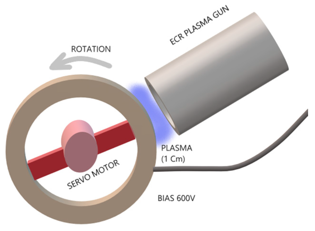
2.1. Coating Process
2.2. Surface Characterization
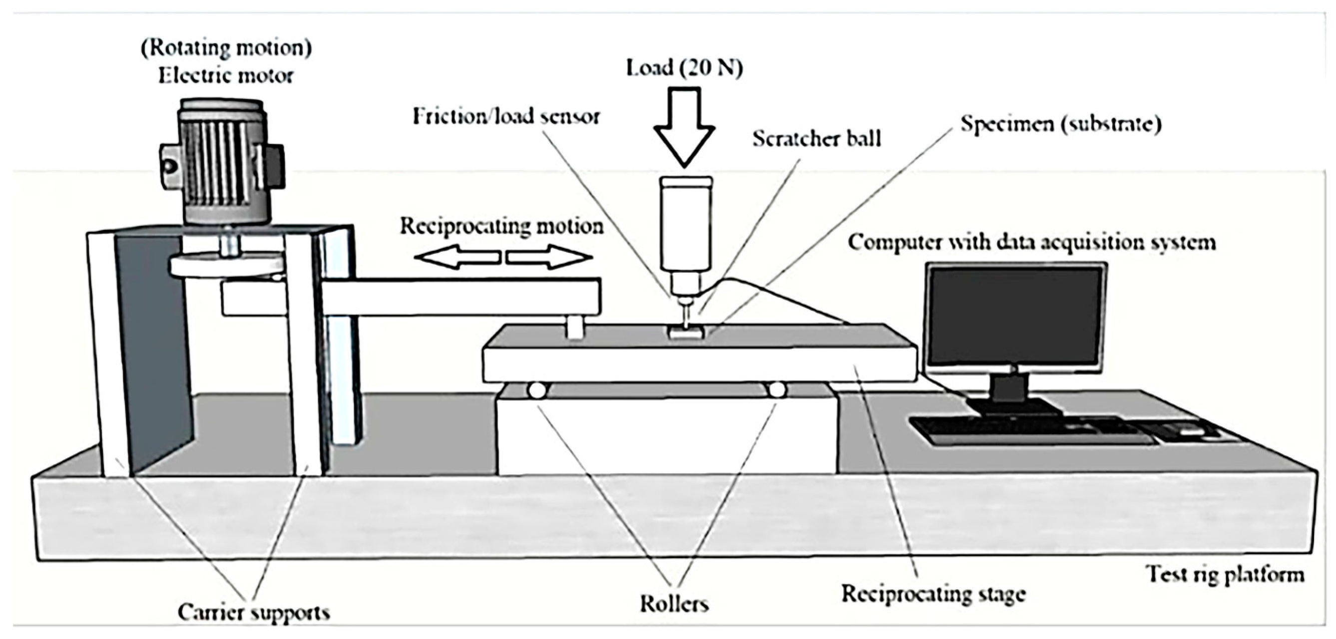
2.3. Mechanical Tests
- Ø: wear rate (mm3/Nm)
- A: trace area (mm2)
- ℓ: amount of reciprocation (mm)
- F: normal load (N)
- s: stroke (m)
2.4. Uncertainty Analysis
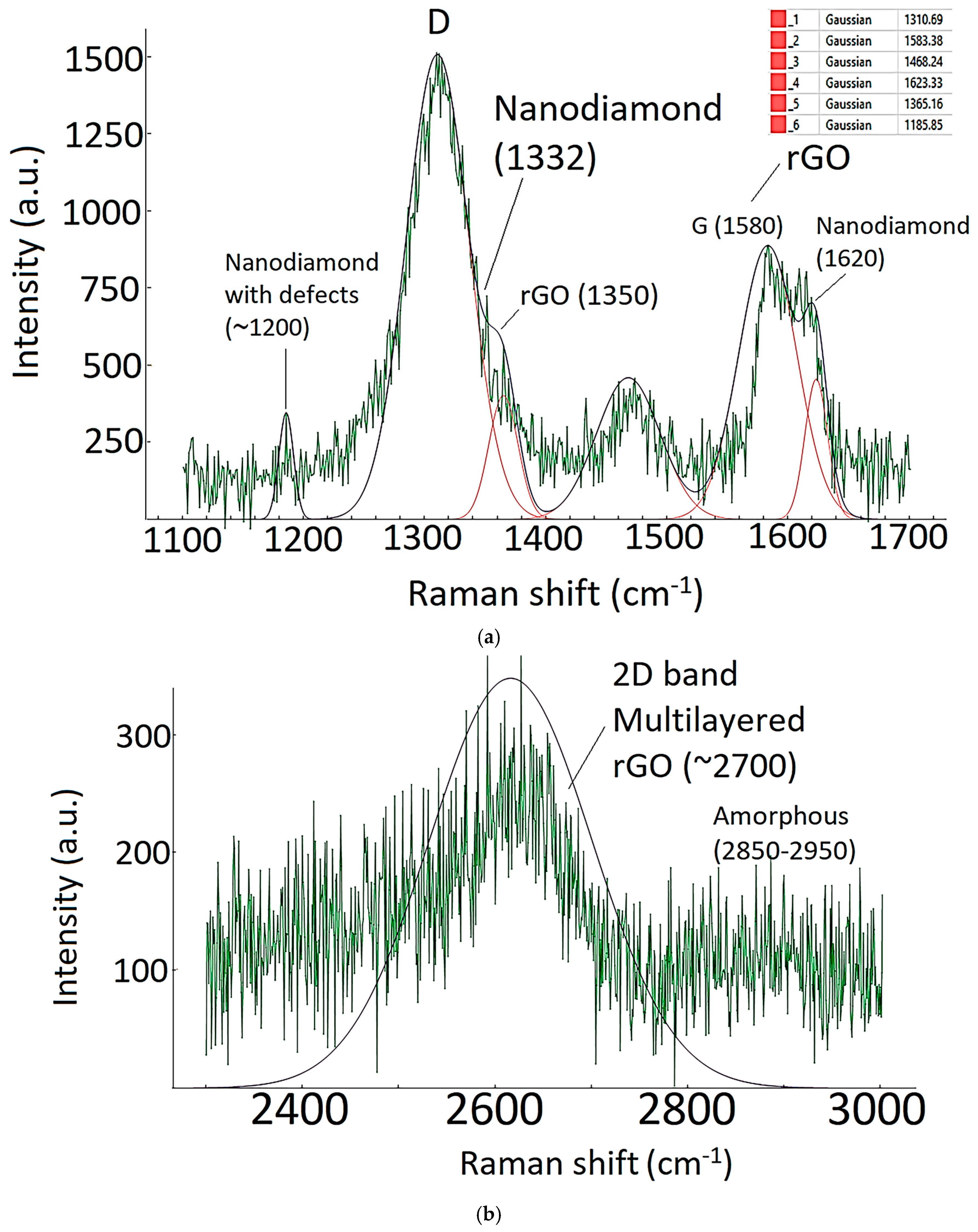
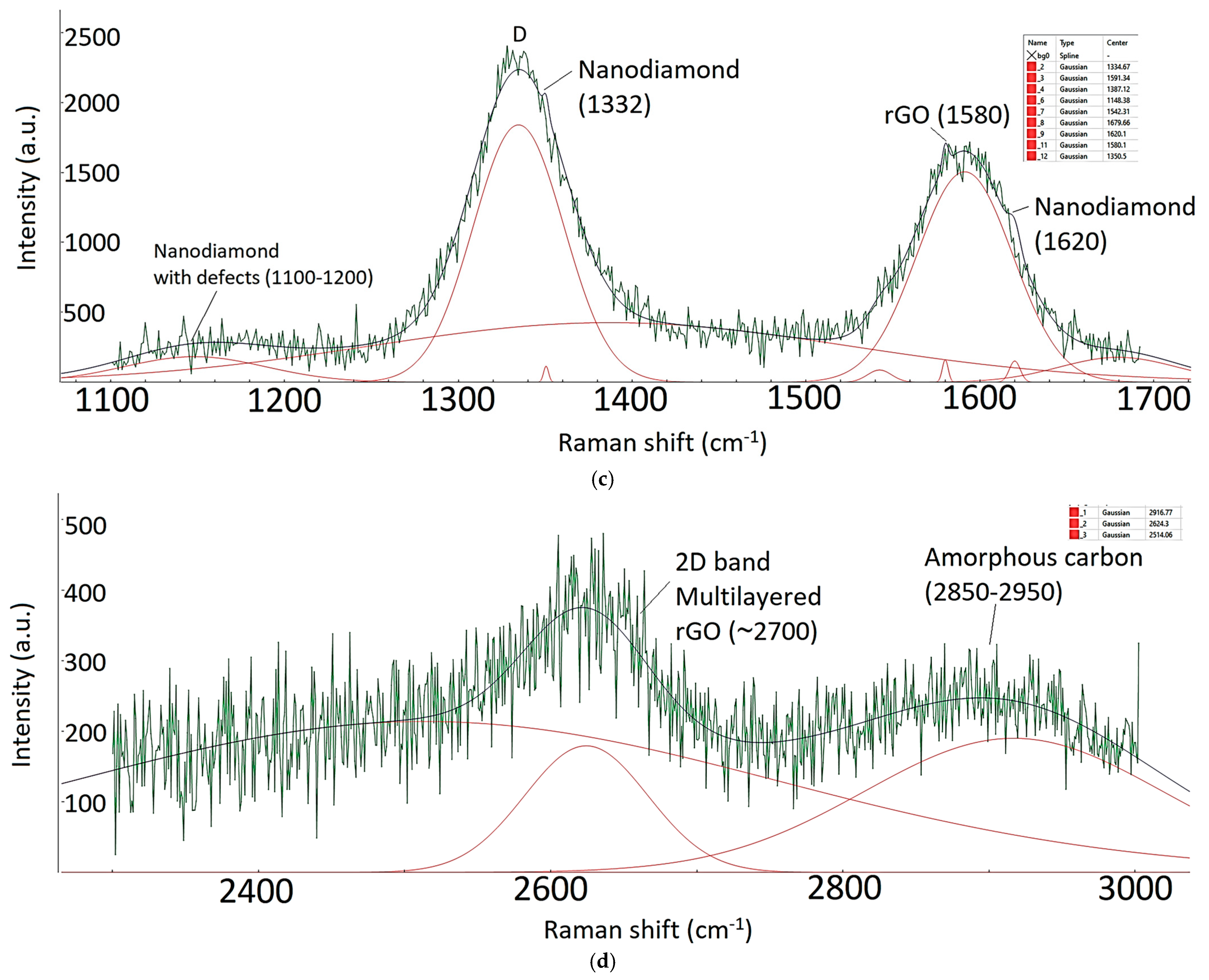
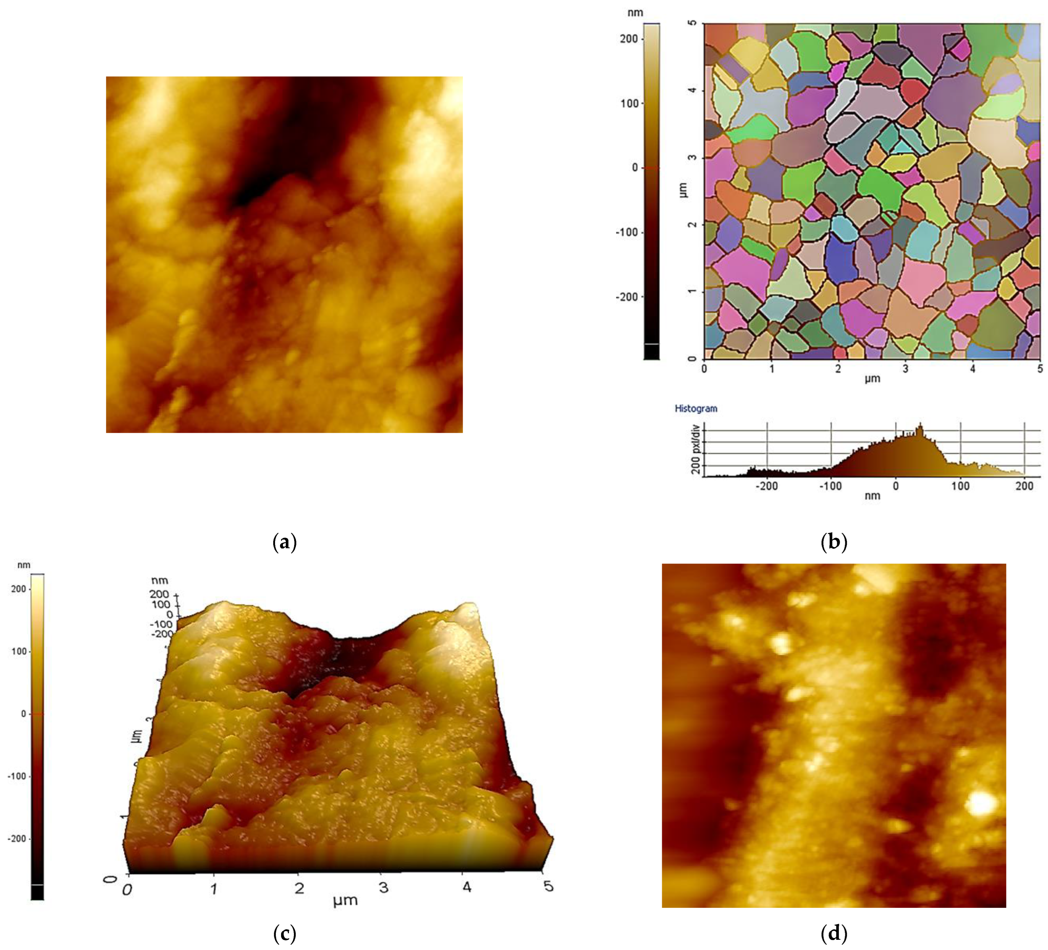
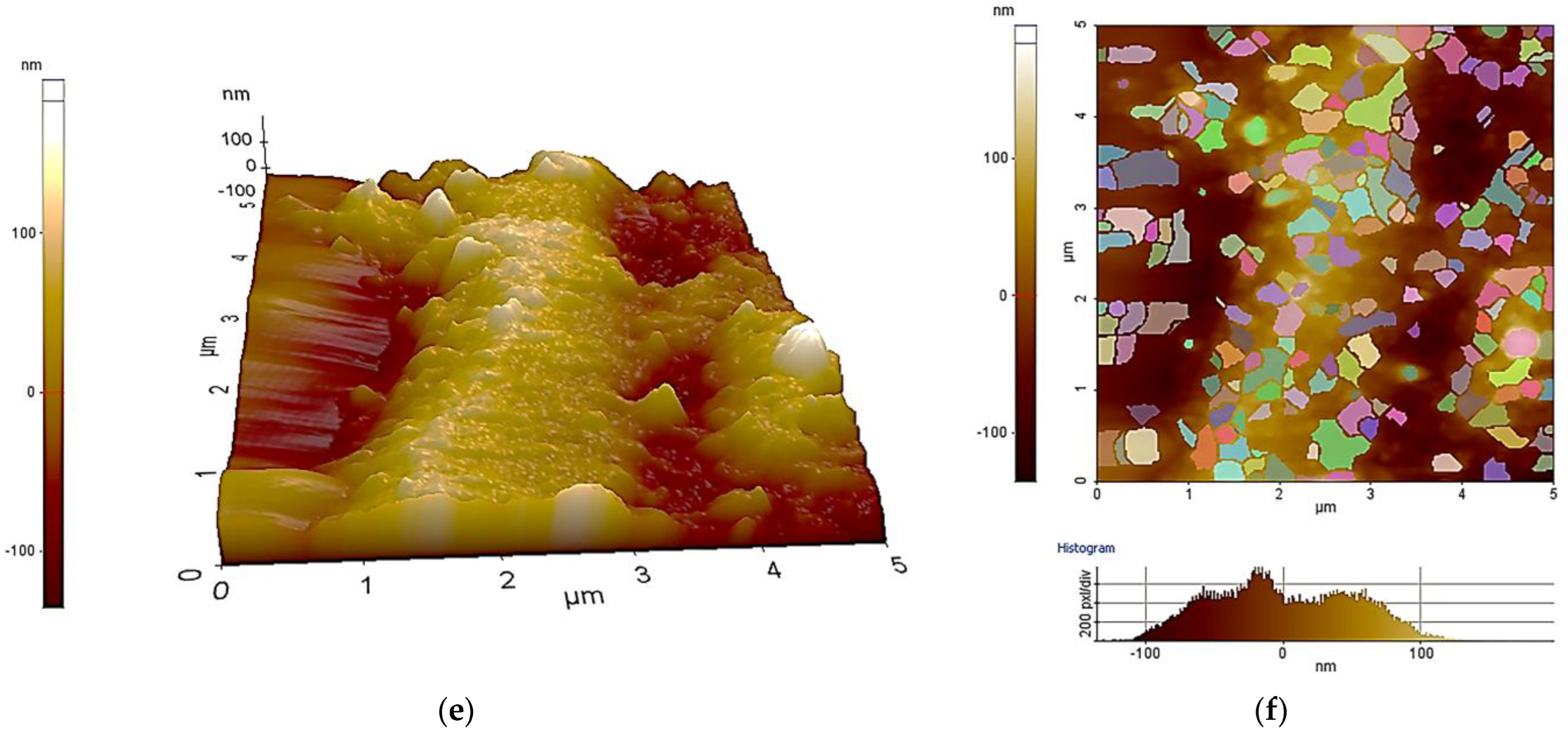
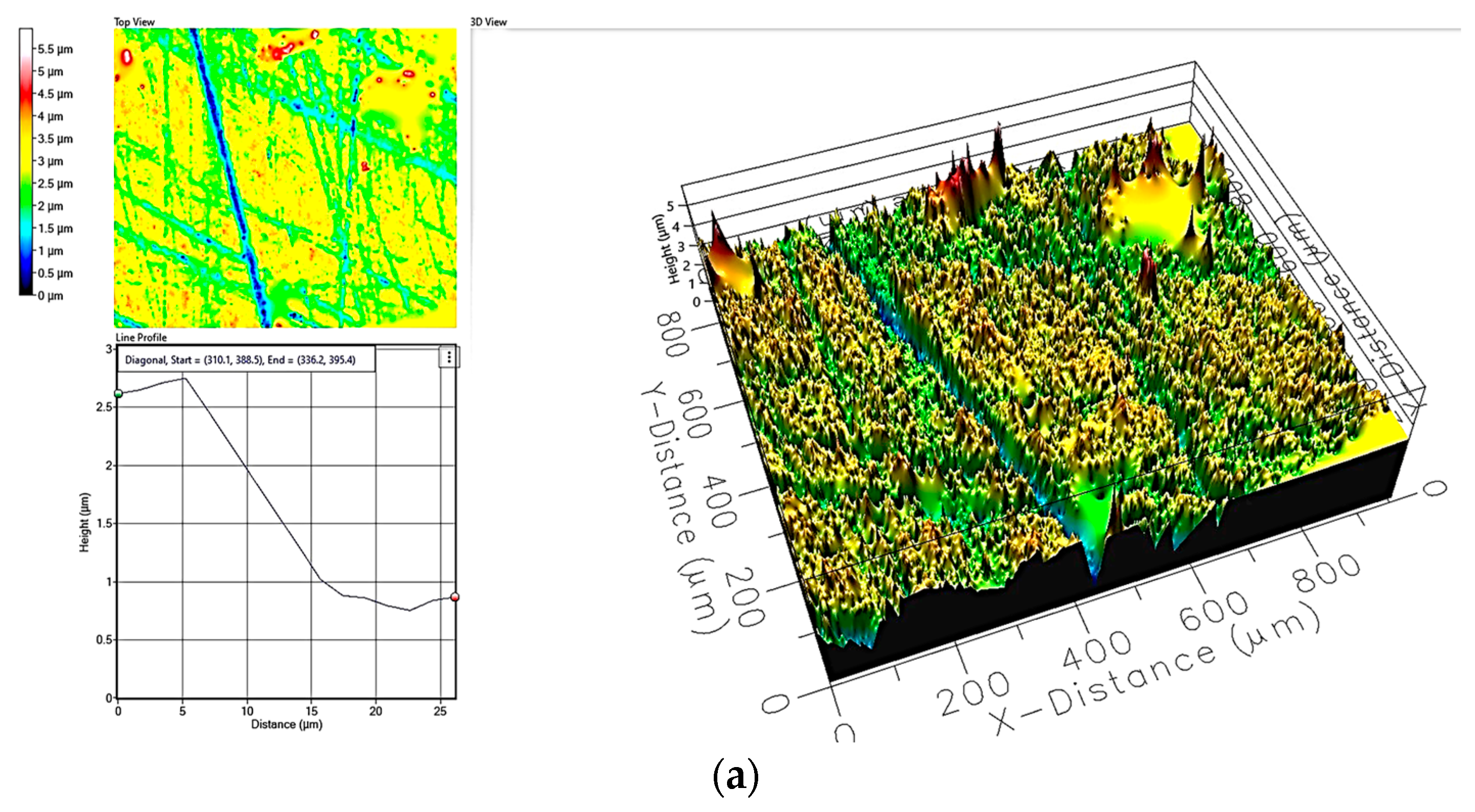
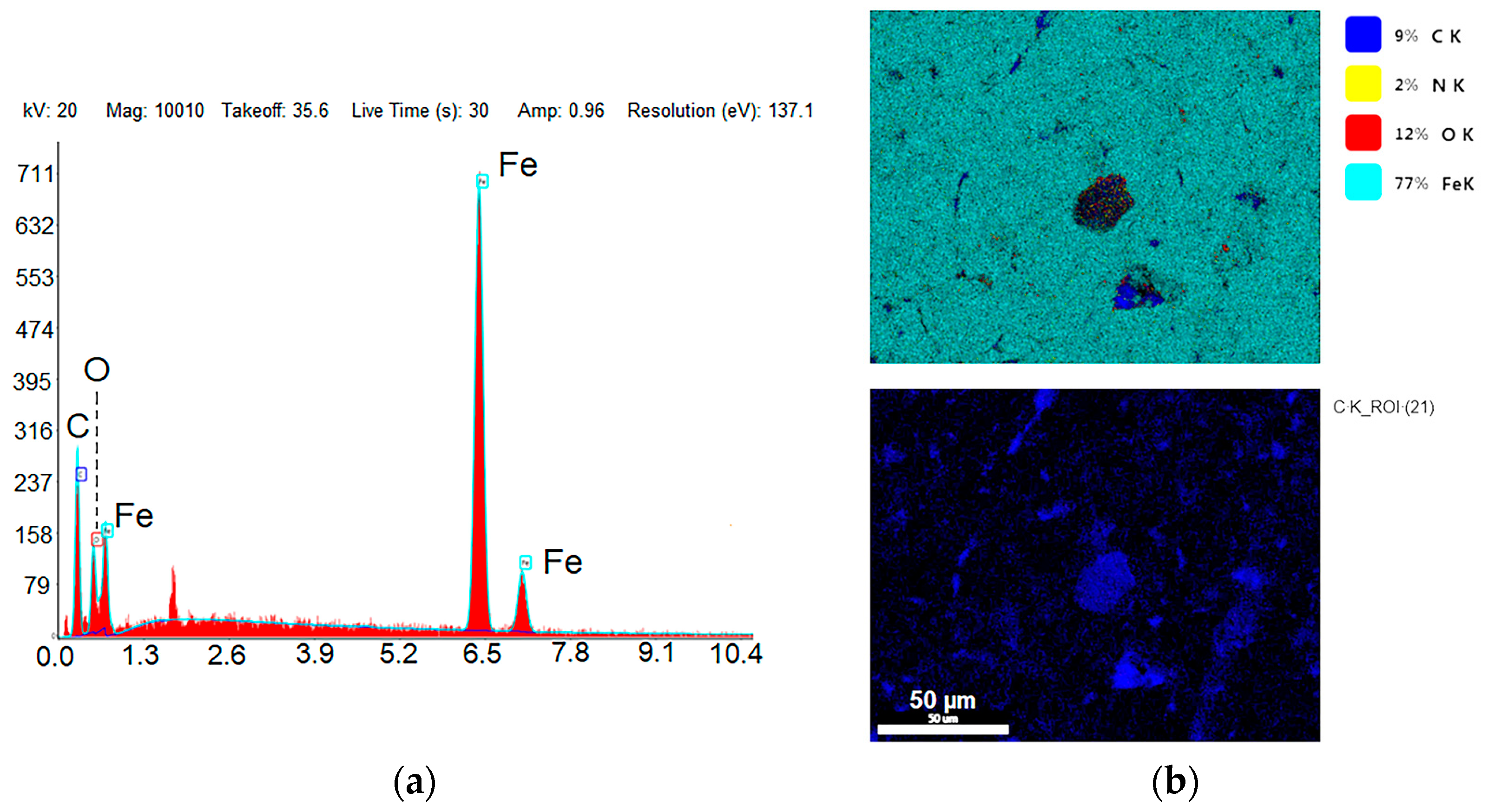
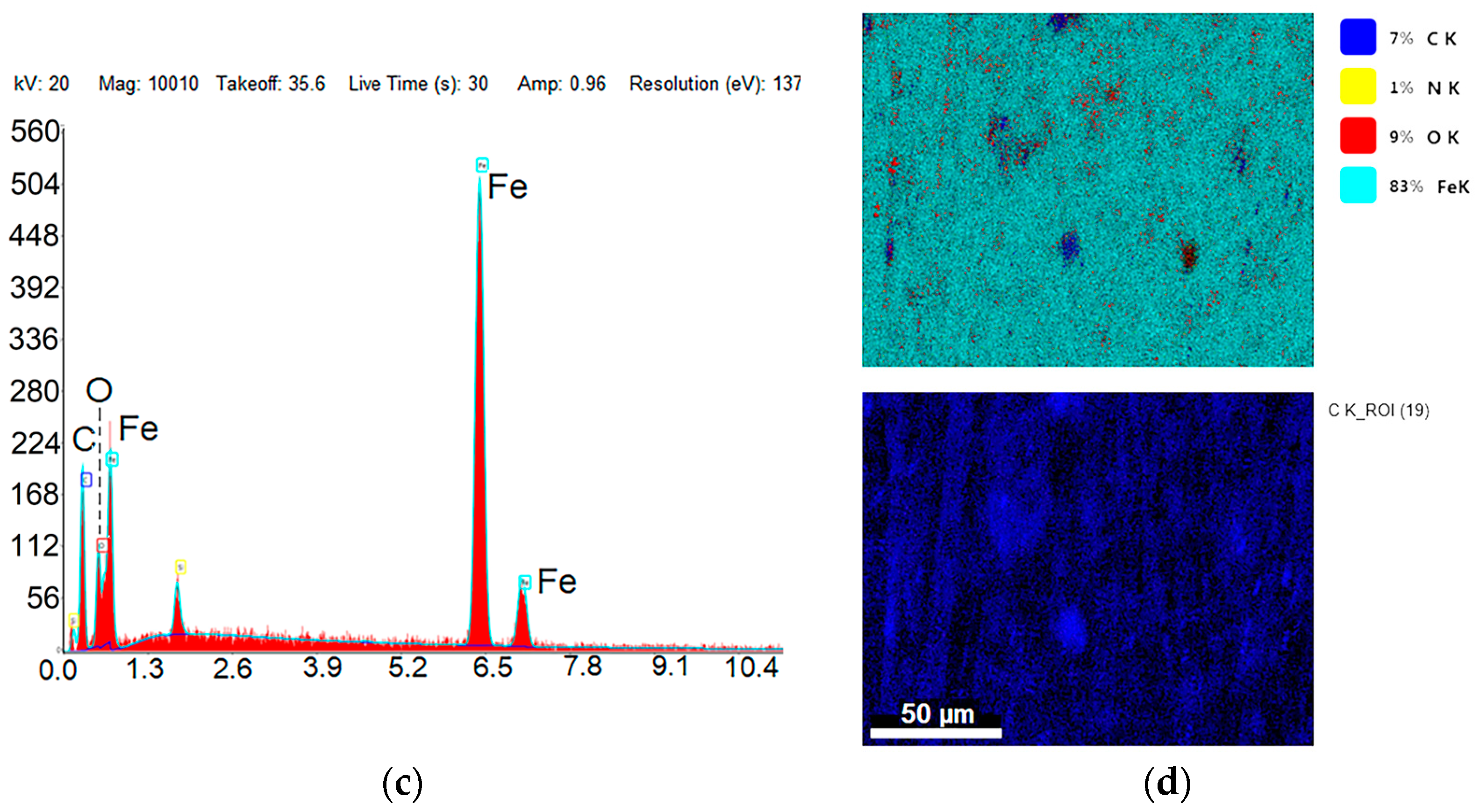
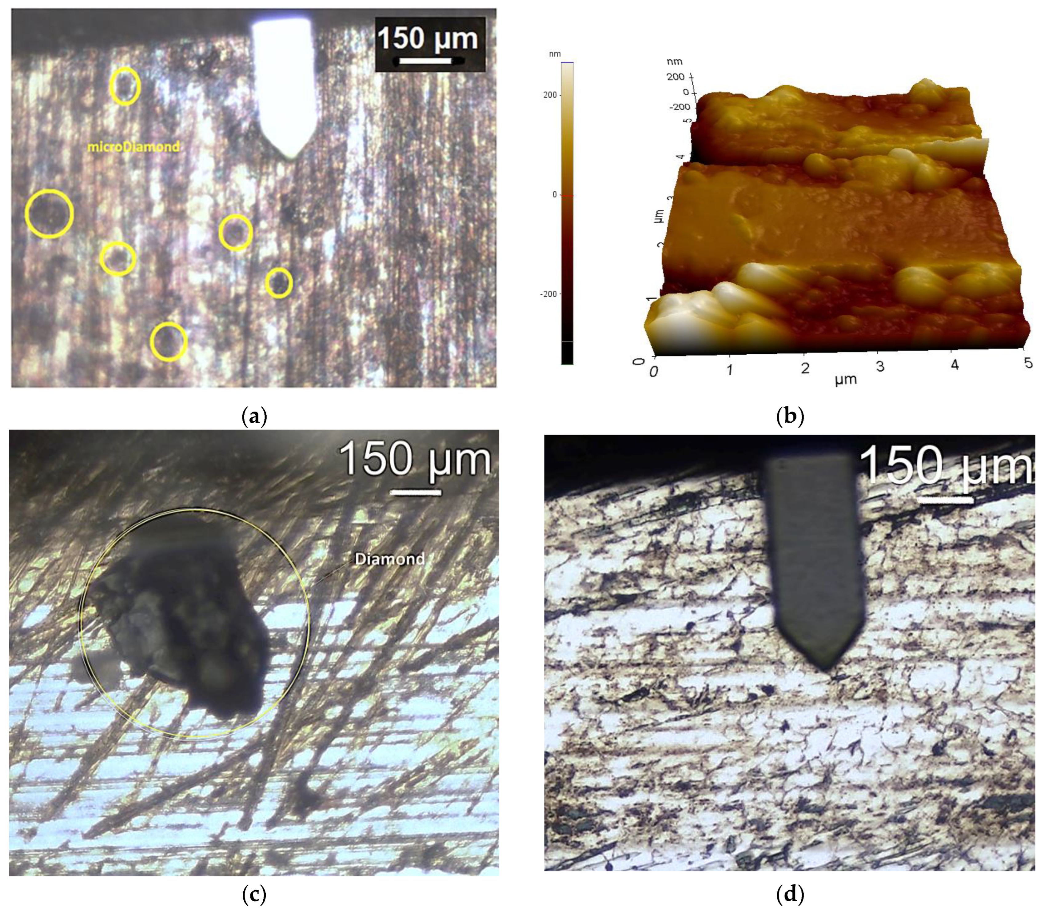
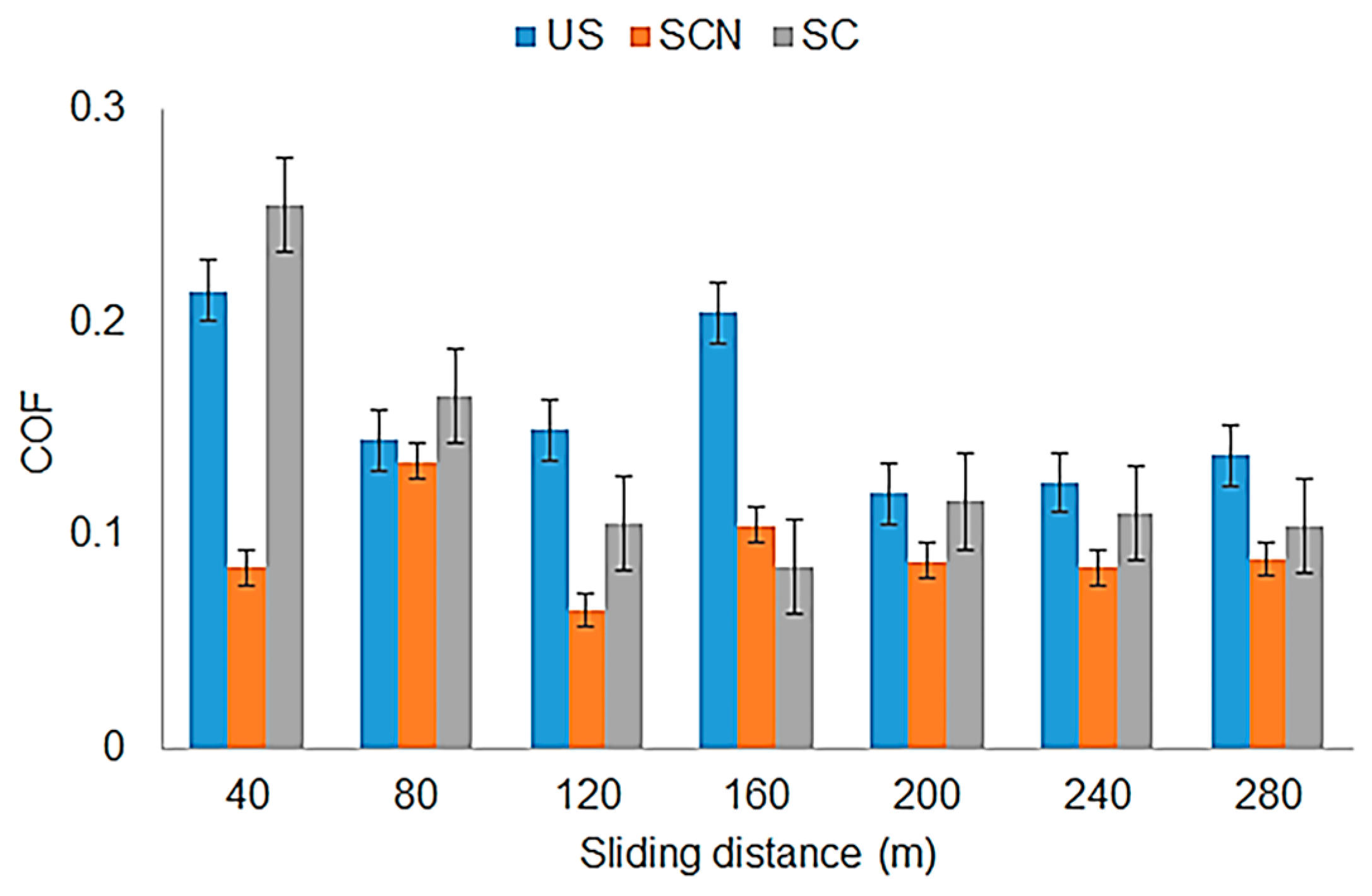
3. Results and Discussion
4. Conclusions
Author Contributions
Funding
Institutional Review Board Statement
Informed Consent Statement
Data Availability Statement
Conflicts of Interest
References
- Al-Jumaili, A.; Alancherry, S.; Bazaka, K.; Jacob, M.V. Review on the Antimicrobial Properties of Carbon Nanostructures. Materials 2017, 10, 1066. [Google Scholar] [CrossRef] [PubMed]
- Erdem Yilmaz, O. Antimicrobial and Gas Adsorption Properties of Electrospun Ferrocene-Polyurethane-Based Nanofibers Containing Silver Nitrate. Arab. J. Sci. Eng. 2023, 48, 389–397. [Google Scholar] [CrossRef]
- Celikel, O.; Kavak, H. Catalyst-Free Carbon Nanowalls Grown on Glass and Silicon Substrates by ECR-MPCVD Method. Diam. Relat. Mater. 2021, 120, 108610. [Google Scholar] [CrossRef]
- Esen, M.; Ilhan, I.; Karaaslan, M.; Unal, E.; Dincer, F.; Sabah, C. Electromagnetic Absorbance Properties of a Textile Material Coated Using Filtered Arc-Physical Vapor Deposition Method. J. Ind. Text. 2015, 45, 298–309. [Google Scholar] [CrossRef]
- Yilmaz, A.C.; Esen, M. Improving Tribological Performance of Piston Ring Steel Substrates by DLC/Nano-Crystalline Diamond Coating. Arab. J. Sci. Eng. 2022, 47, 15441–15453. [Google Scholar] [CrossRef]
- Dresselhaus, M.S.; Dresselhaus, G.; Saito, R.; Jorio, A. Raman Spectroscopy of Carbon Nanotubes. Phys. Rep. 2005, 409, 47–99. [Google Scholar] [CrossRef]
- Pang, H.; Wang, X.; Zhang, G.; Chen, H.; Lv, G.; Yang, S. Characterization of Diamond-like Carbon Films by SEM, XRD and Raman Spectroscopy. Appl. Surf. Sci. 2010, 256, 6403–6407. [Google Scholar] [CrossRef]
- Itoh, T.; Shimabukuro, S.; Kawamura, S.; Nonomura, S. Preparation and Electron Field Emission of Carbon Nanowall by Cat-CVD. Thin Solid Films 2006, 501, 314–317. [Google Scholar] [CrossRef]
- Kar, R.; Patel, N.N.; Chopade, S.S.; Mukherjee, S.; Das, A.K.; Patil, D.S. Bias-Independent Growth of Carbon Nanowalls by Microwave Electron-Cyclotron Resonance Plasma CVD. J. Exp. Nanosci. 2014, 9, 575–581. [Google Scholar] [CrossRef]
- Poluektov, N.P.; Kharchenko, V.N.; Usatov, I.G. Ionization of Sputtered Metal Atoms in a Microwave ECR Plasma Source. Plasma Phys. Reports 2001, 27, 625–633. [Google Scholar] [CrossRef]
- Takehiro, S.; Yamanaka, N.; Shindo, H.; Shingubara, S.; Horiike, Y. Sputtering of Aluminum Film Using Microwave Plasma with High Magnetic Field. Jpn. J. Appl. Phys. 1991, 30, 3657–3661. [Google Scholar] [CrossRef]
- Xiong, Y.; Gao, H.; Ren, N.; Liu, Z. Atomic Layer Deposition of Copper Thin Film and Feasibility of Deposition on Inner Walls of Waveguides. Plasma Sci. Technol. 2018, 20, 035507. [Google Scholar] [CrossRef]
- Gorbatkin, S.M.; Poker, D.B.; Rhoades, R.L.; Doughty, C.; Berry, L.A.; Rossnagel, S.M. Cu Metallization Using a Permanent Magnet Electron Cyclotron Resonance Microwave Plasma/Sputtering Hybrid System. J. Vac. Sci. Technol. B Microelectron. Nanom. Struct. Process. Meas. Phenom. 1996, 14, 1853–1859. [Google Scholar] [CrossRef]
- Holber, W.M.; Logan, J.S.; Grabarz, H.J.; Yeh, J.T.C.; Caughman, J.B.O.; Sugerman, A.; Turene, F.E. Copper Deposition by Electron Cyclotron Resonance Plasma. J. Vac. Sci. Technol. A Vac. Surf. Film. 1993, 11, 2903–2910. [Google Scholar] [CrossRef]
- Aydil, E.S.; Gregus, J.A.; Gottscho, R.A. Electron Cyclotron Resonance Plasma Reactor for Cryogenic Etching. Rev. Sci. Instrum. 1993, 64, 3572–3584. [Google Scholar] [CrossRef]
- Deenamma Vargheese, K.; Mohan Rao, G. Electron Cyclotron Resonance Plasma Source for Ion Assisted Deposition of Thin Films. Rev. Sci. Instrum. 2000, 71, 467–472. [Google Scholar] [CrossRef]
- Srisantirut, T.; Phetchakul, T. Development of Hetero-Junction Cells with a DLC Film Anti-reflection Layer. In Asia Conference on Environment and Sustainable Development; Ujikawa, K., Ishiwatari, M., Hullebusch, E.V., Eds.; Springer Nature: Singapore, 2024. [Google Scholar] [CrossRef]
- Akbari, M.; Kamruddin, M.; Morad, R.; Khamlich, S.; Bucher, R. Characterization of Vertically-Oriented Graphene Nanosheets Grown on Copper Substrate. Mater. Today Proc. 2021, 36, 232–236. [Google Scholar] [CrossRef]
- Kapsiz, M.; Geffroy, S.; Holzer, A.; Schmitz, K. Tribological Performances of Diamond-Like Carbon Coatings for Hydraulic Applications. Chem. Eng. Technol. 2022, 46, 118–127. [Google Scholar] [CrossRef]
- Wang, C.; Wen, F.; Wang, Y.; Guo, W. Structure and Tribological Properties of Multiphase Carbon Coatings Fabricated by Multi-Arc Ion Plating. Surf. Coat. Technol. 2024, 477, 130319. [Google Scholar] [CrossRef]
- Yin, S.; Wu, H.; Yi, X.; Huang, Z.; Ye, C.; Li, P.; Zhang, Y.; Shi, J.; Hua, K.; Wang, H. Enhanced Graphene Oxide Adhesion on Steel Surface Through Boronizing Functionalization Treatment: Toward the Robust Ultralow Friction. Carbon 2023, 206, 201–210. [Google Scholar] [CrossRef]
- Liu, D.H.; Lai, Y.S. Effectiveness of Electromagnetic Interference Shielding of Sputtered Nitrogen-Doped Carbon Thin Films. Diam. Relat. Mater. 2021, 111, 108234. [Google Scholar] [CrossRef]
- Leal, G.; Fraga, M.A.; Rasia, L.A.; Massi, M. Impact of high N2 flow ratio on the chemical and morphological characteristics of sputtered N-DLC films. Surf. Interf. Anal. 2017, 49, 99–106. [Google Scholar] [CrossRef]
- Khanbolouki, P.; Tehrani, M. Purification, Structural Evolutions, and Electrical Properties of Carbon Nanotube Yarns Processed via Incandescent Annealing. Carbon 2020, 168, 710–718. [Google Scholar] [CrossRef]
- Huang, W.; Wang, Y.; Luo, G.; Wei, F. 99.9% Purity Multi-Walled Carbon Nanotubes By Vacuum High-Temperature Annealing. Carbon 2003, 41, 2585–2590. [Google Scholar] [CrossRef]
- Sundaram, R.; Yamada, T.; Hata, K.; Sekiguchi, A. Purifying Carbon Nanotube Wires by Vacuum Annealing. Mater. Today Proc. 2018, 5, 27316–27326. [Google Scholar] [CrossRef]
- Niven, J.F.; Johnson, M.B.; Juckes, S.M.; White, M.A.; Alvarez, N.T.; Shanov, V. Influence of Annealing on Thermal and Electrical Properties of Carbon Nanotube Yarns. Carbon 2016, 99, 485–490. [Google Scholar] [CrossRef]
- Mohammed, A.; Abdullah, A. Scanning Electron Microscopy (SEM): A Review. In Proceedings of the 2018 International Conference on Hydraulics and Pneumatics—HERVEX, Băile Govora, Romania, 7–9 November 2018; pp. 77–85. [Google Scholar]
- Orlando, A.; Franceschini, F.; Muscas, C.; Pidkova, S.; Bartoli, M.; Rovere, M.; Tagliaferro, A. A Comprehensive Review on Raman Spectroscopy Applications. Chemosensors 2021, 9, 262. [Google Scholar] [CrossRef]
- Bunaciu, A.A.; Udristioiu, E.G.; Aboul-Enein, H.Y. X-Ray Diffraction: Instrumentation and Applications. Crit. Rev. Anal. Chem. 2015, 45, 289–299. [Google Scholar] [CrossRef]
- Benea, L.; Basa, S.; Danaila, E.; Caron, N.; Raquet, O.; Ponthiaux, P.; Celis, J. Fretting and Wear Behaviors of Ni/Nano-WC Composite Coatings in Dry and Wet Conditions. Mat. Des. 2015, 65, 550–558. [Google Scholar] [CrossRef]
- Subramanian, B.; Thangavel, V. Experimental Investigations on Performance, Emission and Combustion Characteristics of Diesel-Hydrogen and Diesel-HHO Gas in A Dual Fuel CI Engine. Int. J. Hydrogen Energy 2020, 45, 25479–25492. [Google Scholar] [CrossRef]
- Albers, P.W.; Leich, V.; Ramirez-Cuesta, A.J.; Cheng, Y.; Hönig, J.; Parker, S.F. The Characterization of Commercial 2D Carbons: Graphene, Graphene Oxide and Reduced Graphene Oxide. Mater. Adv. 2022, 3, 2810–2826. [Google Scholar] [CrossRef]
- Ferrari, A.C.; Basko, D.M. Raman Spectroscopy as a Versatile Tool for Studying the Properties of Graphene. Nature Nanotechnol. 2013, 8, 235–246. [Google Scholar] [CrossRef]
- Gates, B.C. Highly Conductive Graphene Oxide-Based Papers. Nature Nanotechnol. 2009, 3, 481–485. [Google Scholar] [CrossRef]
- Kharisov, B.I.; Kharissova, O.V.; Chávez-Guerrero, L. Synthesis Techniques, Properties, and Applications of Nanodiamonds. Synth. React. Inorg. Met. -Org. Nano-Met. Chem. 2010, 40, 84–101. [Google Scholar]
- Mermoux, M.; Chang, S.; Girard, H.A.; Arnault, J.C. Raman Spectroscopy Study of Detonation Nanodiamond. Diam. Rel. Mater. 2018, 15, 522–525. [Google Scholar] [CrossRef]
- Jorio, A.; Filho, A.G.S. Raman Studies of Carbon Nanostructures. Annu. Rev. Mater. Res. 2016, 46, 357–382. [Google Scholar] [CrossRef]
- Karczemska, A.; Szurgot, M.; Kozanecki, M.; Szynkowska, M.I.; Ralchenko, V.; Danilenko, V.V.; Louda, P.; Mitura, S. Extraterrestrial, Terrestrial and Laboratory Diamonds-Differences and Similarities. Diam. Relat. Mater. 2008, 17, 1179–1185. [Google Scholar] [CrossRef]
- Scardaci, V.; Compagnini, G. Raman Spectroscopy Investigation of Graphene Oxide Reduction by Laser Scribing. C 2021, 7, 48. [Google Scholar] [CrossRef]
- King, A.A.K.; Davies, B.R.; Noorbehesht, N.; Newman, P.; Church, T.L.; Harris, A.T.; Razal, J.M.; Minett, A.I. A New Raman Metric for the Characterization of Graphene Oxide and Its Derivatives. Sci. Rep. 2016, 6, 19491. [Google Scholar] [CrossRef]
- Kaniyoor, A.; Ramaprabhu, S. A Raman Spectroscopic Investigation of Graphite Oxide Derived Graphene. AIP Adv. 2012, 2, 032183. [Google Scholar] [CrossRef]
- Chu, P.K.; Li, L. Characterization of Amorphous and Nanocrystalline Carbon Films. Mater. Chem. Phys. 2006, 96, 253–277. [Google Scholar] [CrossRef]
- Fedoseeva, Y.V.; Pozdnyakov, G.A.; Okotrub, A.V.; Kanygin, M.A.; Nastaushev, Y.V.; Vilkov, O.Y.; Bulusheva, L.G. Effect of Substrate Temperature on the Structure of Amorphous Oxygenated Hydrocarbon Films Grown with a Pulsed Supersonic Methane Plasma Flow. Appl. Surf. Sci. 2016, 385, 464–471. [Google Scholar] [CrossRef]
- Yang, B.; Yu, B.; Li, H.; Huang, N.; Liu, L.; Jiang, X. Enhanced and Switchable Silicon-Vacancy Photoluminescence in Air-Annealed Nanocrystalline Diamond Films. Carbon 2020, 156, 242–252. [Google Scholar] [CrossRef]
- Yasin, G.; Arif, M.; Shakeel, M.; Dun, Y.; Zuo, Y.; Khan, W.Q.; Tang, Y.; Khan, A.; Nadeem, M. Exploring the Nickel–Graphene Nanocomposite Coatings for Superior Corrosion Resistance: Manipulating the Effect of Deposition Current Density on Its Morphology, Mechanical Properties, and Erosion-Corrosion Performance. Adv. Eng. Mater. 2018, 20, 1701166. [Google Scholar] [CrossRef]
- Cicala, G.; Magaletti, V.; Carbone, G.; Senesi, G.S. Load Sensitive Super-Hardness of Nanocrystalline Diamond Coatings. Diam. Relat. Mater. 2020, 101, 107653. [Google Scholar] [CrossRef]
- Pusty, M.; Sharma, A.; Sinha, L.; Chaudhary, A.; Shirage, P. Comparative Study with a Unique Arrangement to Tap Piezoelectric Output to Realize a Self-Poled PVDF Based Nanocomposite for Energy Harvesting Applications. ChemistrySelect 2017, 2, 2774–2782. [Google Scholar] [CrossRef]
- Iyer, M.S.; Wang, F.M.; Jayapalan, R.R.; Veeramani, S.; Rajangam, I. RGO Based Immunosensor Amplified Using MWCNT and CNF Nanocomposite as Analytical Tool for CA125 Detection. Anal. Biochem. 2021, 634, 114393. [Google Scholar] [CrossRef]
- Drewniak, S.; Muzyka, R.; Stolarczyk, A.; Pustelny, T.; Kotyczka-Morańska, M.; Setkiewicz, M. Studies of Reduced Graphene Oxide and Graphite Oxide in the Aspect of Their Possible Application in Gas Sensors. Sensors 2016, 16, 103. [Google Scholar] [CrossRef]
- Krishnamoorthy, K.; Veerapandian, M.; Yun, K.; Kim, S.J. The Chemical and Structural Analysis of Graphene Oxide with Different Degrees of Oxidation. Carbon 2013, 53, 38–49. [Google Scholar] [CrossRef]
- Zeng, A.; Yin, Y.; Bilek, M.; McKenzie, D. Ohmic Contact to Nitrogen Doped Amorphous Carbon Films. Surf. Coat. Technol. 2005, 198, 202–205. [Google Scholar] [CrossRef]
- Li, J.; Kim, S.J.; Han, S.; Chae, H. Characterization of sp2/sp3 Hybridization Ratios of Hydrogenated Amorphous Carbon Films Deposited in C2H2 Inductively Coupled Plasmas. Surf. Coat. Technol. 2021, 422, 127514. [Google Scholar] [CrossRef]


| Sample ID | Process | Process Pressure (Torr) | N2 Flow Rate (sccm) | CH4 Flow Rate (sccm) | Plasma Current (mA) | Bias Voltage (V) | Rotation Rate (°/min) | Process Duration (min) | Coating Thickness (µm) |
|---|---|---|---|---|---|---|---|---|---|
| US | Etching | 7.0 ± 0.5 × 10⁻³ | 11.28 ± 1.0 | - | 26 | −580 ± 30 | 5 | 60 ± 2 | - |
| SCN | Coating | 5.1 ± 0.2 × 10⁻³ | 11.00 ± 1.0 | 6.82 | 26 | −580 ± 20 | 5 | 60 ± 2 | 2.72 ± 0.2 |
| SC | Coating | 5.2 ± 0.2 × 10⁻³ | - | 6.74 | 26 | −580 ± 20 | 5 | 60 ± 2 | 3.55 ± 0.2 |
| Analysis | Device | Technical Specs |
|---|---|---|
| Laser-cutting | Senfeng (Jinan City, China) | Laser power: 1.5–3 kW Positioning accuracy: ±0.05 mm Max. speed: 80 m/min |
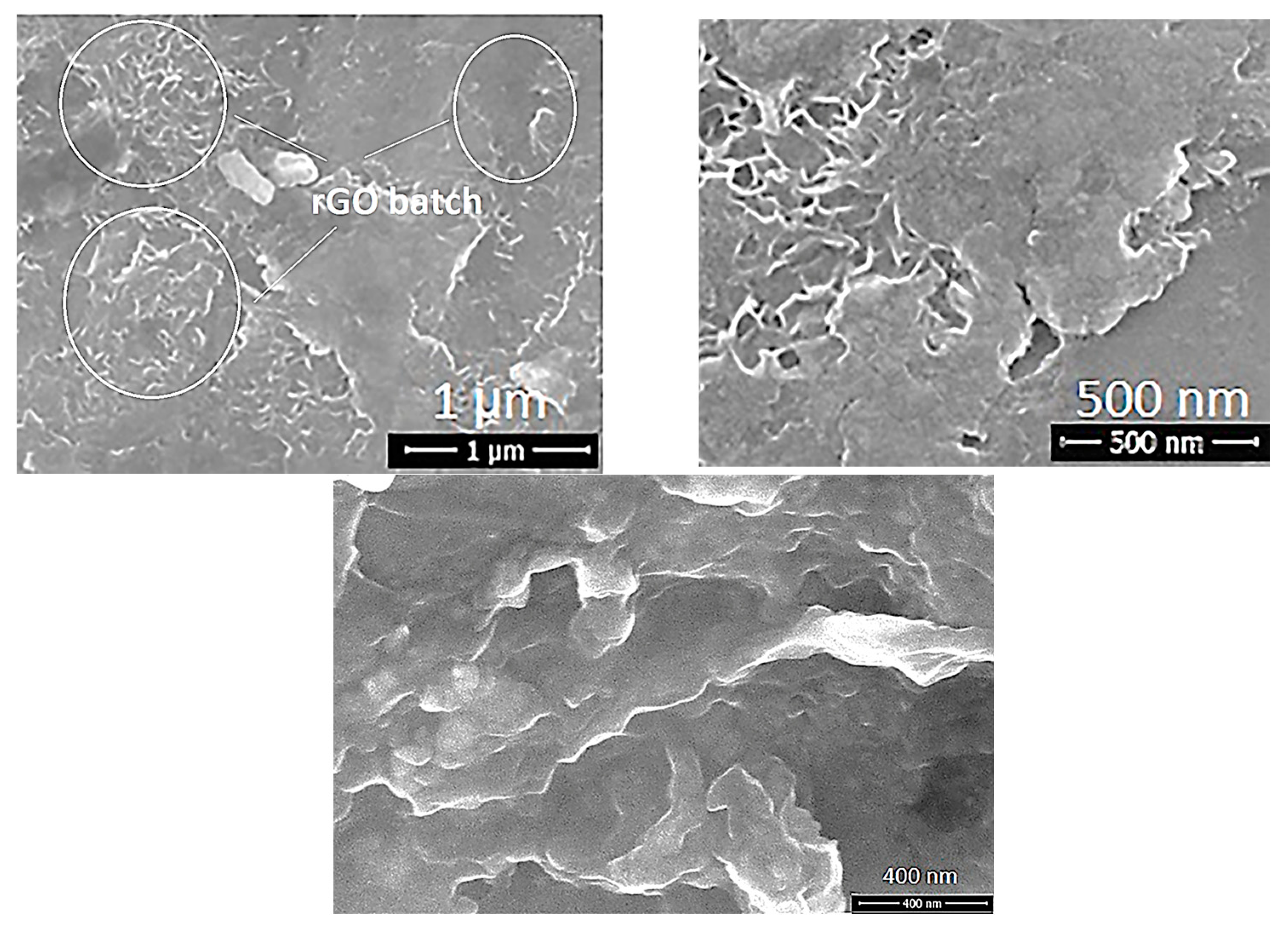
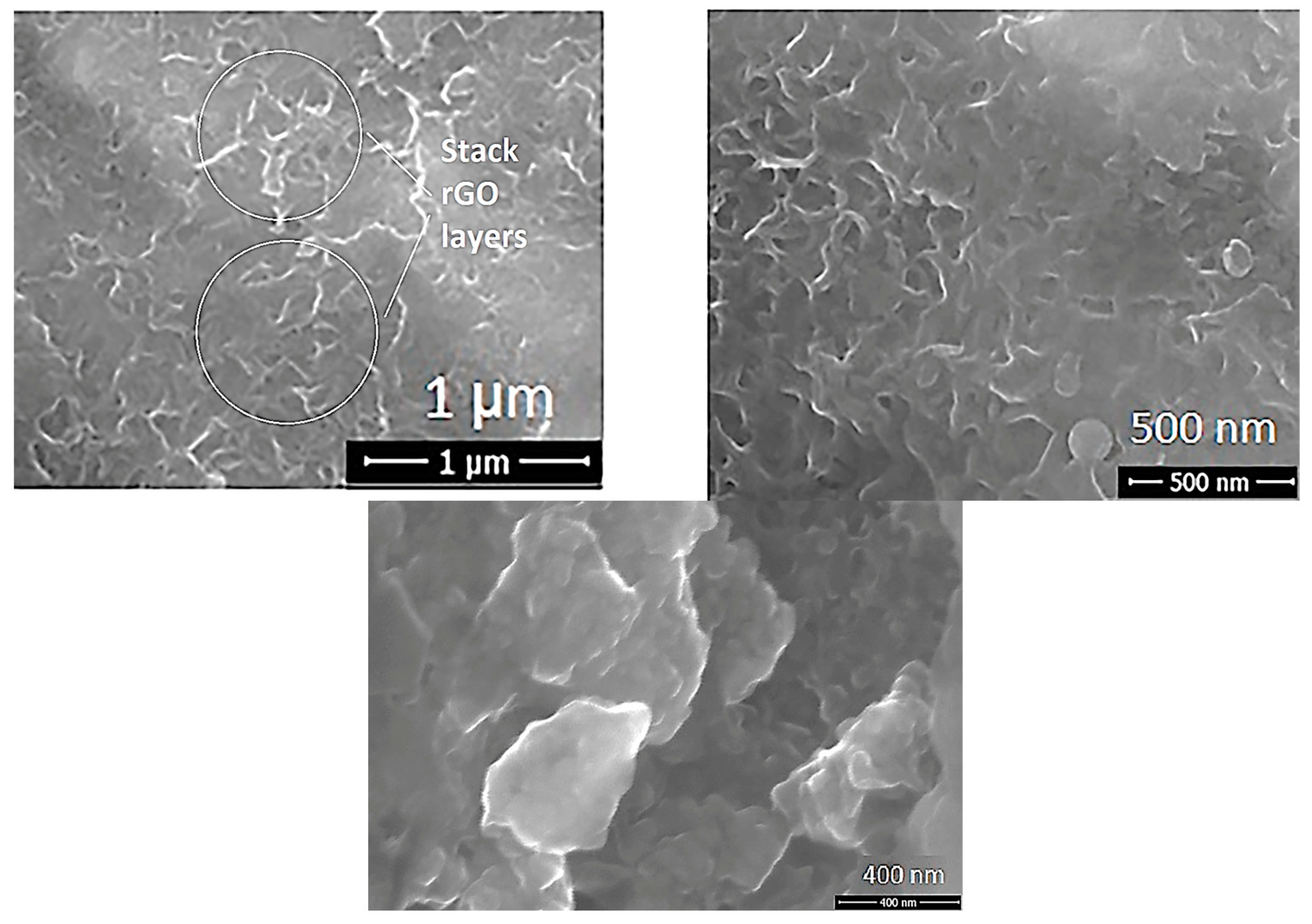
| SEM and EDX | FEI Quanta 650 (Hillsboro, OR, USA) | Resolution: 1.2 nm @ 30 kV Magnification: 6–106× |
| XRD | Rigaku Miniflex II (Tokyo, Japan) | X-ray source: Cu anode (λ Cu Kα = 1.5418 Å), Measurement range (2θ) = 2–145° |
| Raman | Renishaw In Via Qontor (Wotton-under-Edge, UK) | Wavelength range: 200–2200 nm Lasers: 229–1064 nm Stability: <±0.01 cm−1 |
| AFM | Park Systems NX10 (Suwon, Republic of Korea) | Field of view: 480 × 360 µm (10× objective lens) CCD: 5 MP |
| Profilometer | Filmetrics Profilm 3D (Quezon City, Philippines) | Thickness range: 50–10 mm Camera: 2592 × 1944 (5 MP) |
| Variable | Error (%) |
|---|---|
| COF | ±1.6 |
| ϕ | ±2.2 |
| Ra | ±2.5 |
| Hardness | ±3.7 |
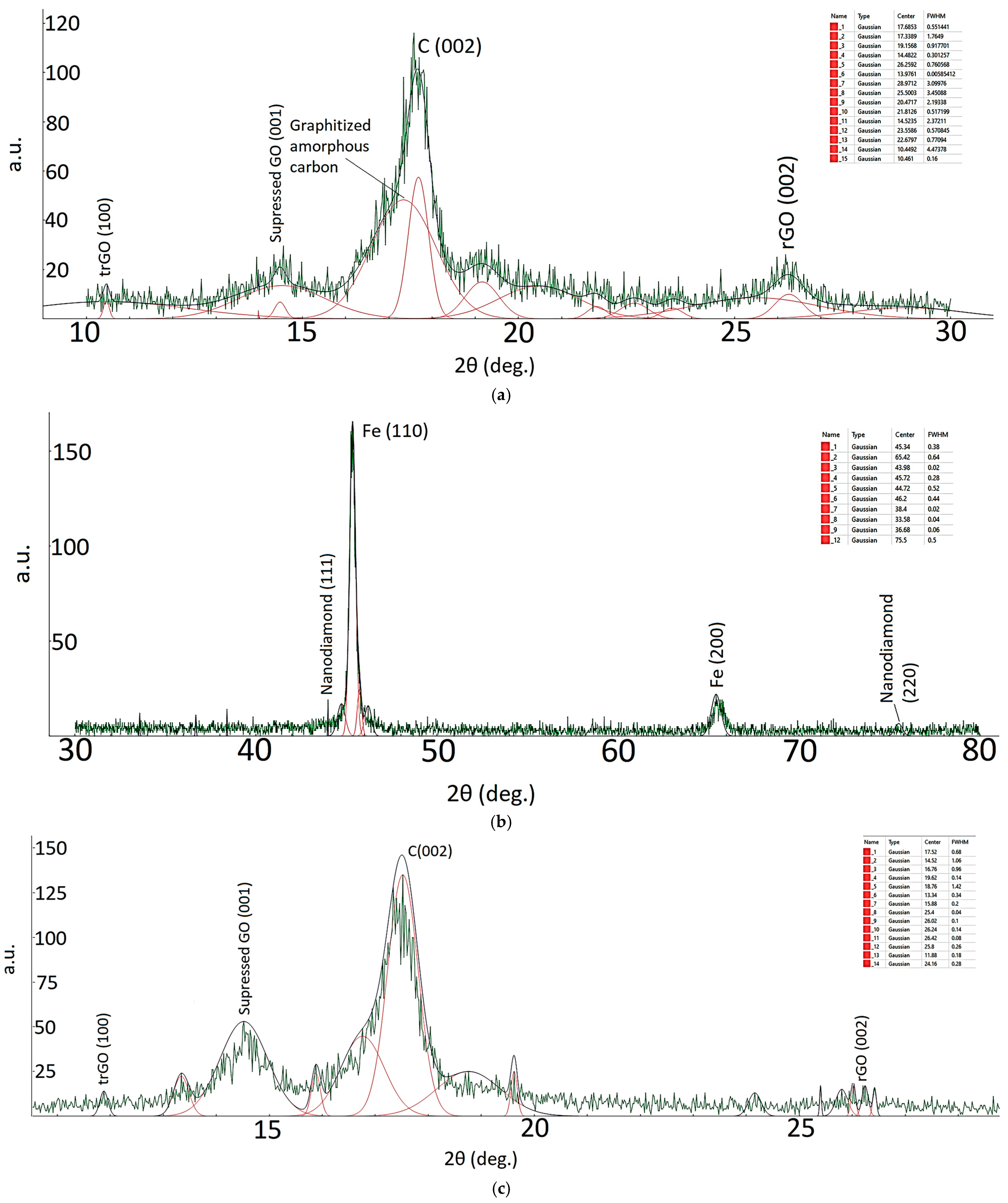
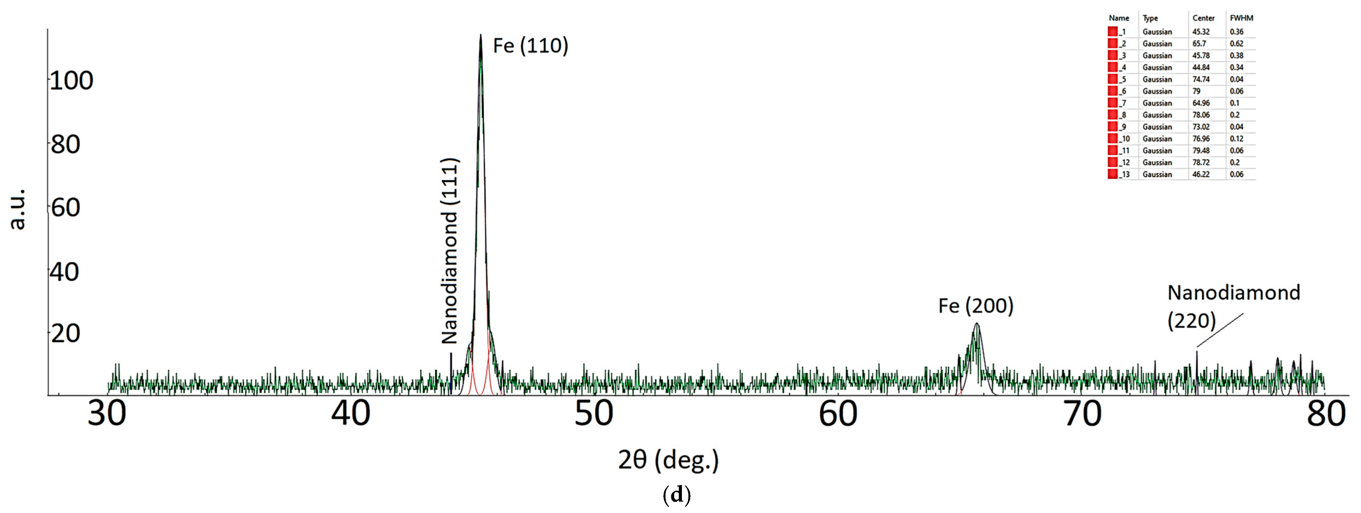
| 2Ɵ | FWMH (°) | Grain Size (nm) |
|---|---|---|
| 10.44 | 4.47 | 1.86 |
| 14.48 | 0.30 | 27.87 |
| 17.33 | 0.55 | 15.25 |
| 26.26 | 0.76 | 11.21 |
| 43.98 | 0.02 | 447.27 |
| 75.5 | 0.02 | 524.59 |
| 2Ɵ | FWMH (°) | Grain Size (nm) |
|---|---|---|
| 11.88 | 0.18 | 46.33 |
| 14.52 | 1.06 | 7.89 |
| 16.76 | 0.96 | 8.73 |
| 26.02 | 0.1 | 85.13 |
| 45.78 | 0.38 | 23.69 |
| 73.02 | 0.04 | 258.03 |
| US (Before N2 Etching) | SC | SCN | ||||
|---|---|---|---|---|---|---|
| Element | Weight % | Atomic % | Weight % | Atomic % | Weight % | Atomic % |
| C | 16.86 | 44.67 | 29.35 | 59.41 | 27.06 | 55.74 |
| N | - | - | 2.42 | 4.24 | 3.64 | 6.37 |
| O | 4.87 | 9.68 | 7.3 | 10.61 | 7.42 | 12.54 |
| Si | 1.89 | 2.14 | 1.52 | 1.44 | 1.41 | 1.16 |
| Fe | 76.37 | 43.5 | 59.41 | 24.3 | 60.45 | 24.2 |
| Ø × 10−9(mm3/Nm) | Hardness (HV) | Roughness (μm) | ||||||||||||||
|---|---|---|---|---|---|---|---|---|---|---|---|---|---|---|---|---|
| Ra | Rz | Av. | Av. | σ | σ | |||||||||||
| 1 | 2 | 3 | Av. | σ | No.1 | No.2 | No.3 | No.1 | No.2 | No.3 | Ra | Rz | Ra | Rz | ||
| US | 37.2 | 264 | 254 | 250 | 256 | 5.89 | 0.83 | 0.64 | 0.74 | 5.32 | 4.53 | 4.73 | 0.74 | 4.86 | 0.09 | 0.41 |
| SCN | 12.5 | 293 | 287 | 292 | 291 | 2.63 | 0.26 | 0.31 | 0.37 | 2.08 | 2.69 | 2.79 | 0.31 | 2.52 | 0.06 | 0.38 |
| SC | 16.1 | 280 | 272 | 273 | 275 | 3.56 | 0.35 | 0.36 | 0.43 | 2.83 | 2.61 | 3.07 | 0.38 | 2.85 | 0.04 | 0.23 |
Disclaimer/Publisher’s Note: The statements, opinions and data contained in all publications are solely those of the individual author(s) and contributor(s) and not of MDPI and/or the editor(s). MDPI and/or the editor(s) disclaim responsibility for any injury to people or property resulting from any ideas, methods, instructions or products referred to in the content. |
© 2025 by the authors. Licensee MDPI, Basel, Switzerland. This article is an open access article distributed under the terms and conditions of the Creative Commons Attribution (CC BY) license (https://creativecommons.org/licenses/by/4.0/).
Share and Cite
Esen, M.; Yilmaz, A.C.; Kavak, H. Structural and Tribological Analysis of Multilayer Carbon-Based Nanostructures Deposited via Modified Electron Cyclotron Resonance–Chemical Vapor Deposition. Appl. Sci. 2025, 15, 3402. https://doi.org/10.3390/app15063402
Esen M, Yilmaz AC, Kavak H. Structural and Tribological Analysis of Multilayer Carbon-Based Nanostructures Deposited via Modified Electron Cyclotron Resonance–Chemical Vapor Deposition. Applied Sciences. 2025; 15(6):3402. https://doi.org/10.3390/app15063402
Chicago/Turabian StyleEsen, Mehmet, Ali Can Yilmaz, and Hamide Kavak. 2025. "Structural and Tribological Analysis of Multilayer Carbon-Based Nanostructures Deposited via Modified Electron Cyclotron Resonance–Chemical Vapor Deposition" Applied Sciences 15, no. 6: 3402. https://doi.org/10.3390/app15063402
APA StyleEsen, M., Yilmaz, A. C., & Kavak, H. (2025). Structural and Tribological Analysis of Multilayer Carbon-Based Nanostructures Deposited via Modified Electron Cyclotron Resonance–Chemical Vapor Deposition. Applied Sciences, 15(6), 3402. https://doi.org/10.3390/app15063402