
Enhanced Linearity in Intracranial Pressure Monitoring System Through Sample Isolation Bridge ROIC


Abstract
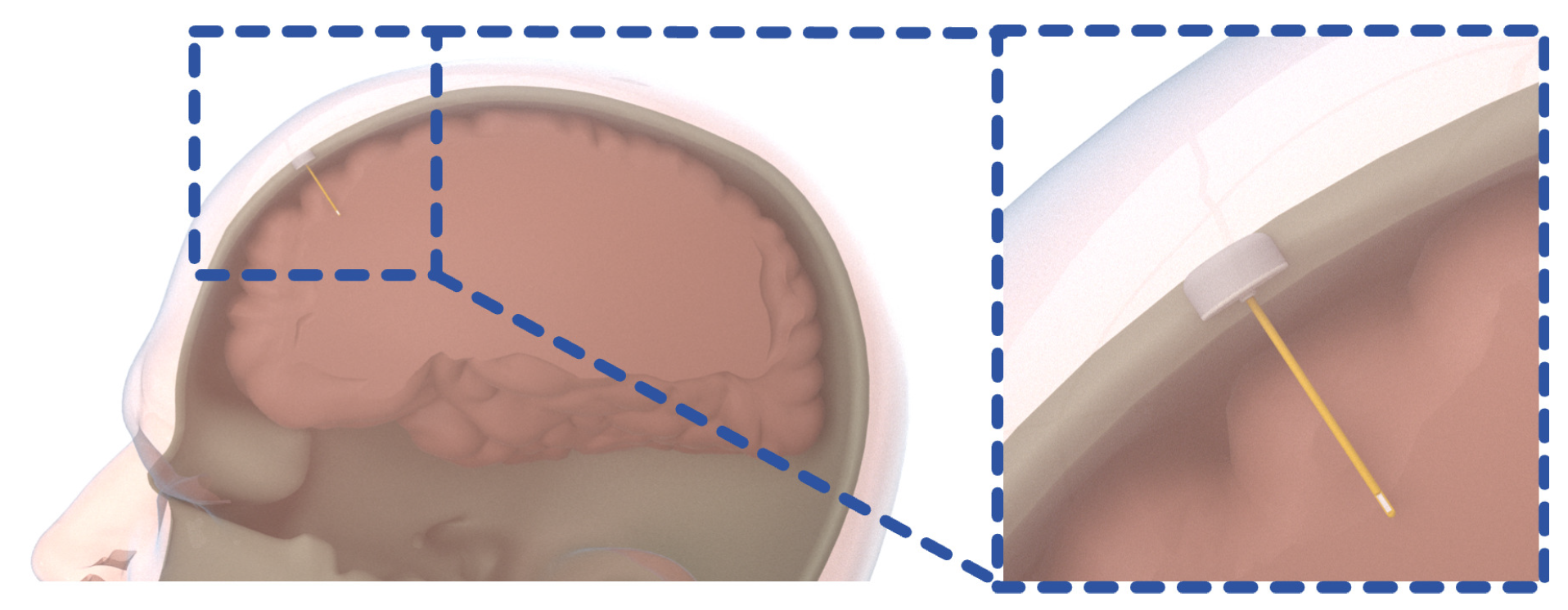
1. Introduction
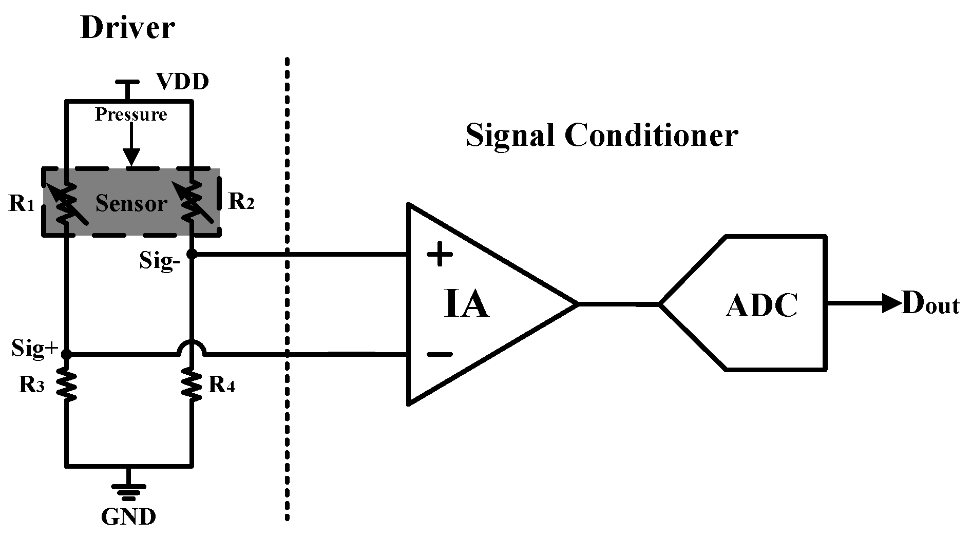
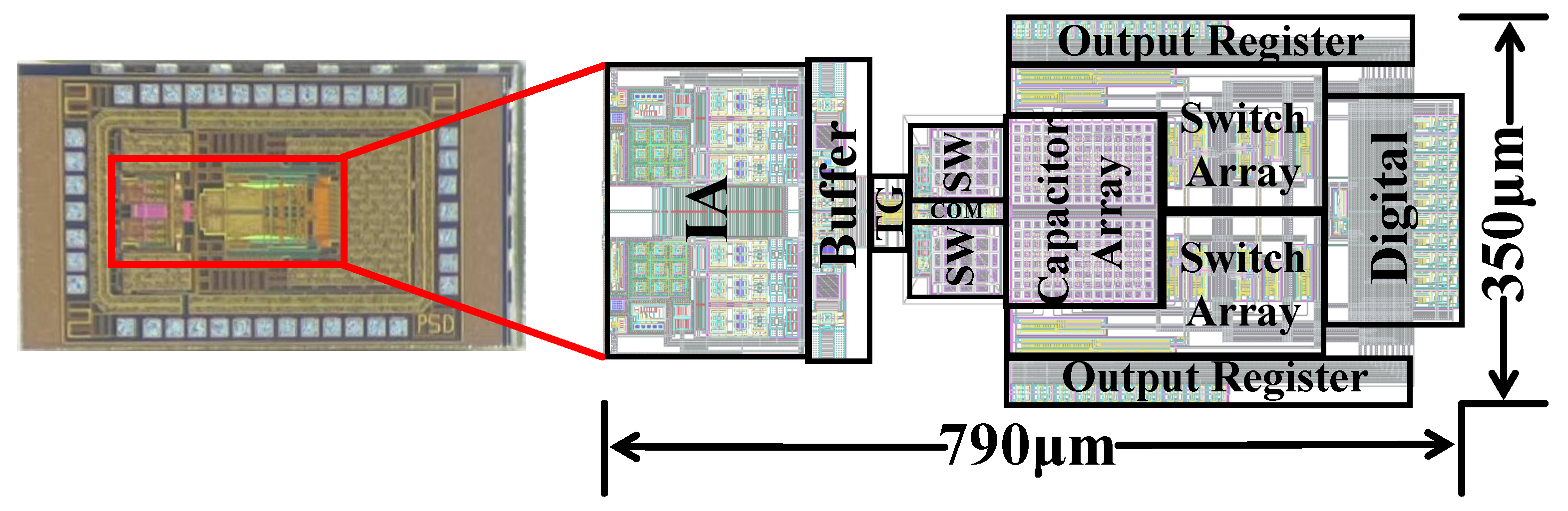
2. System Design of the ROIC
3. ROIC Implementation Details
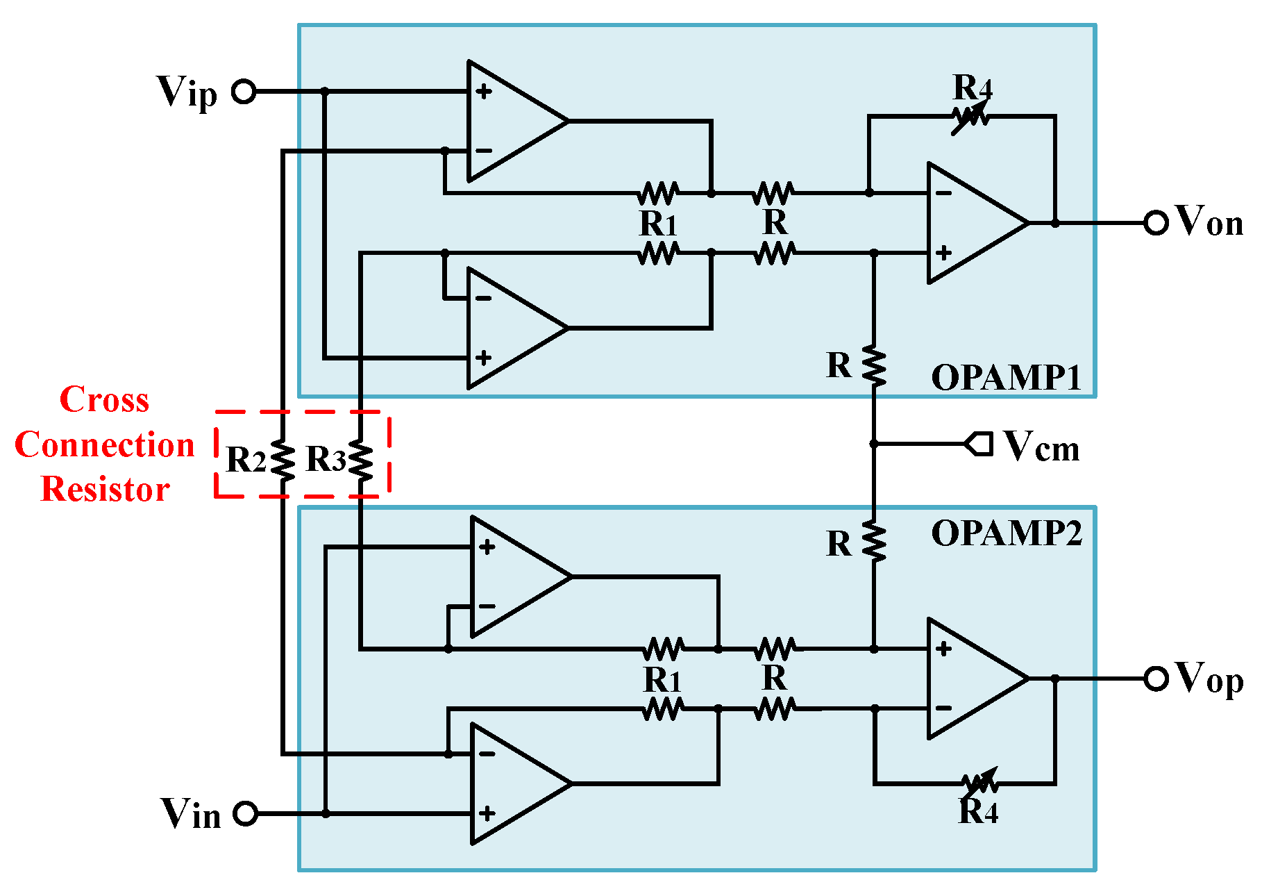
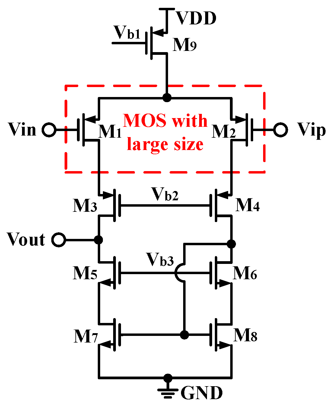
3.1. Cross-Connection Instrumentation Amplifier Scheme
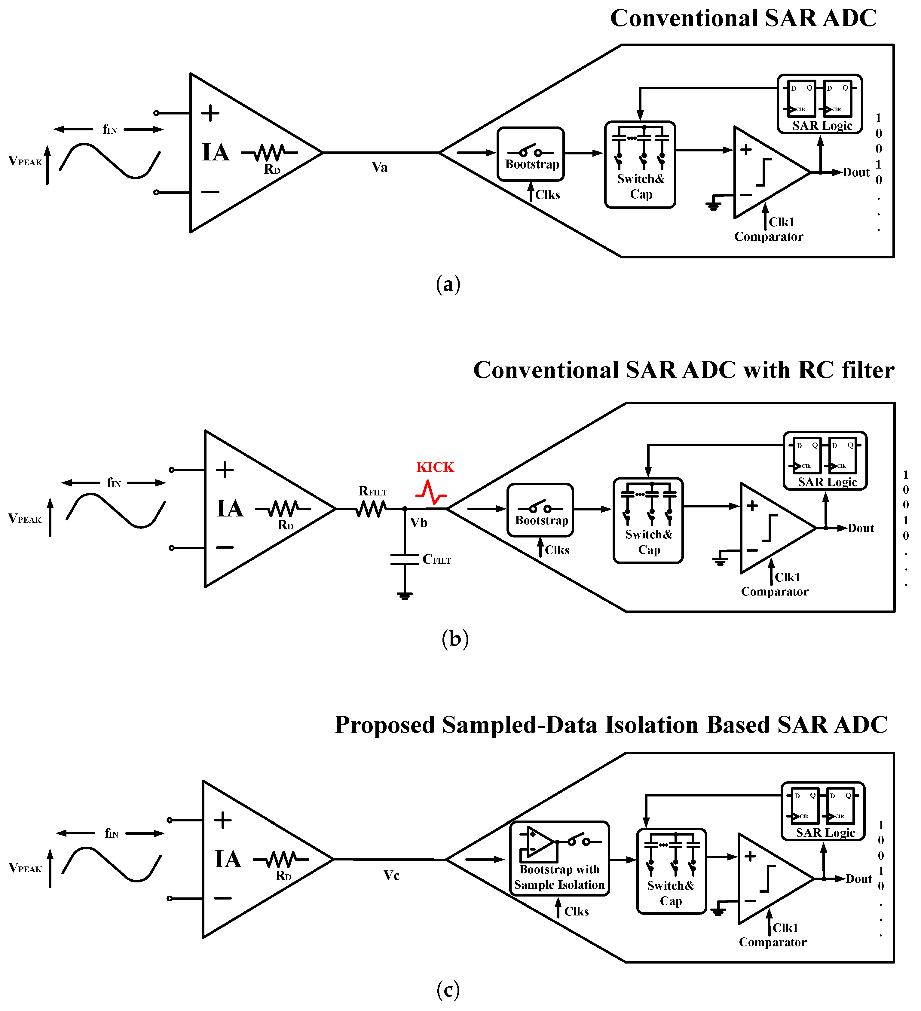
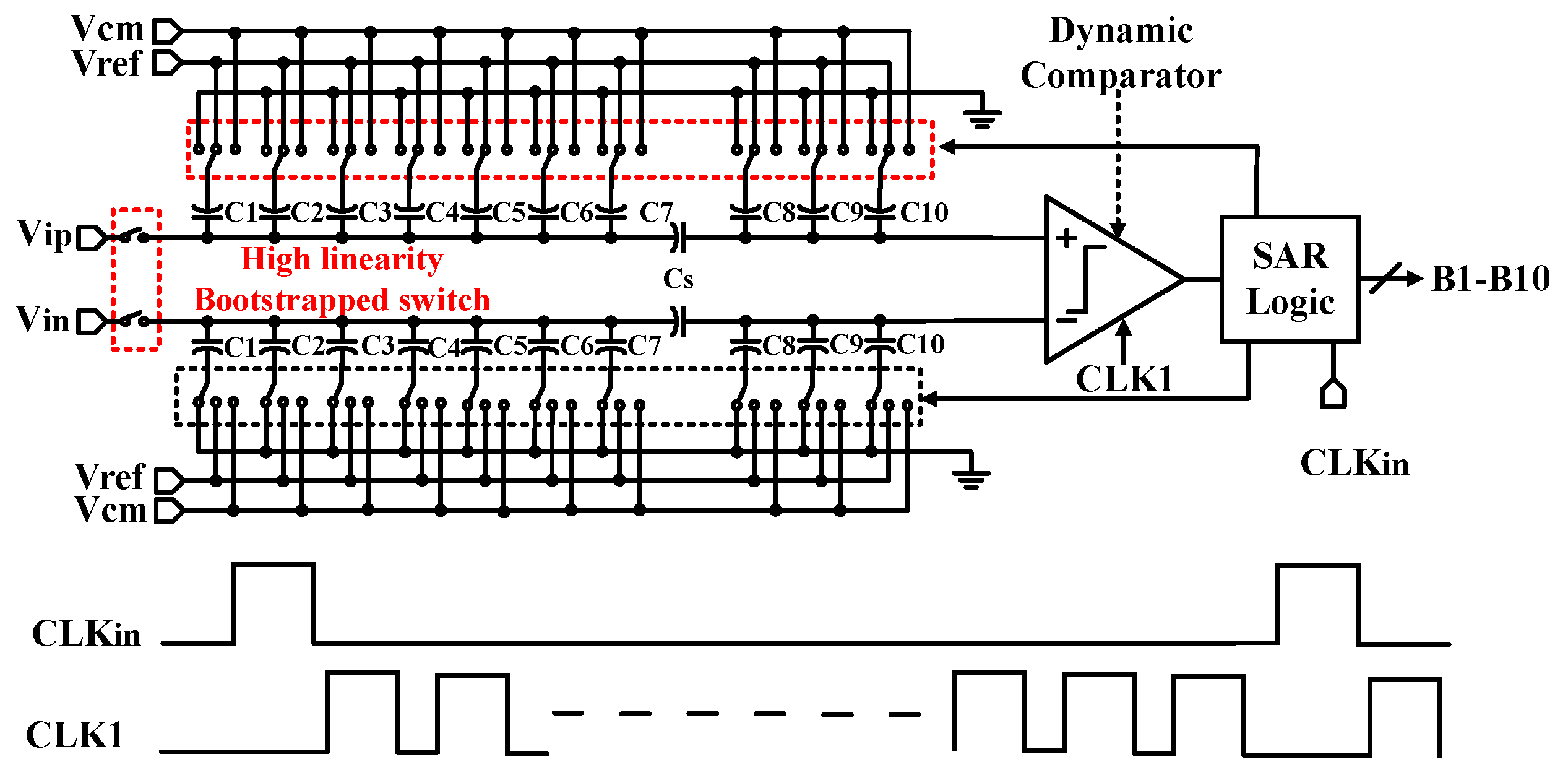
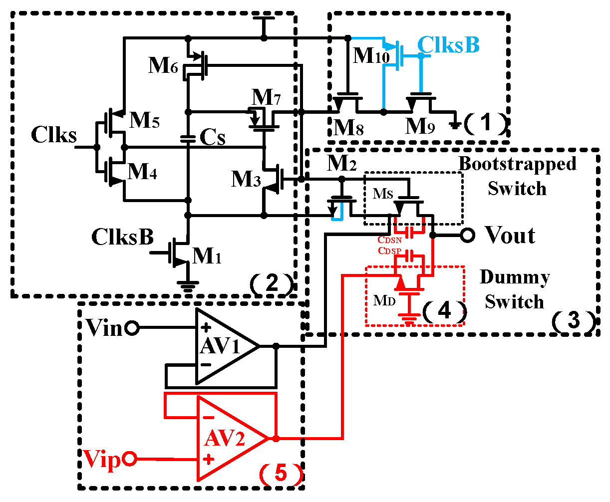
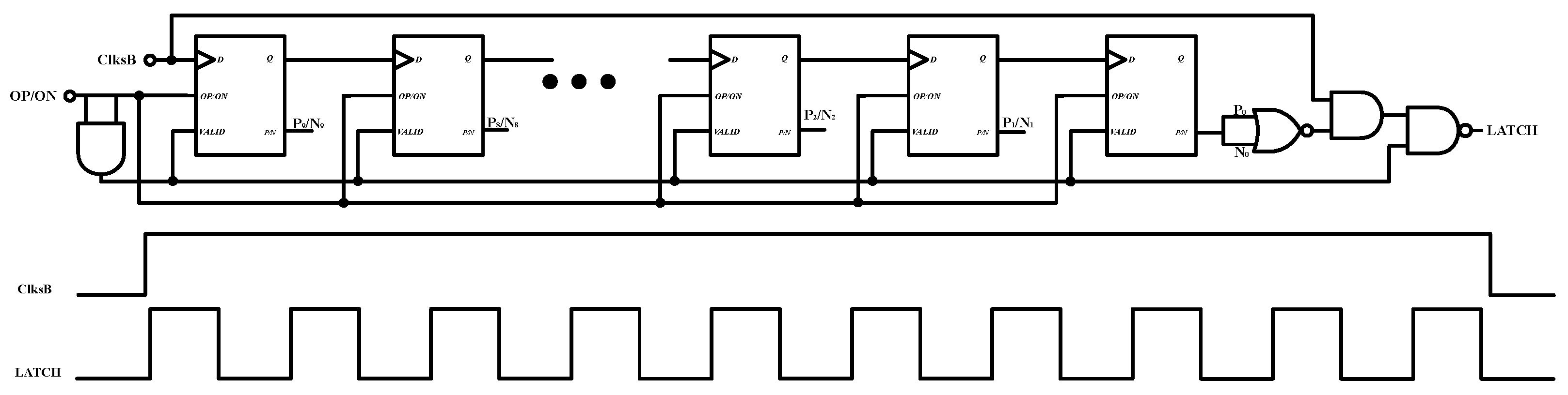
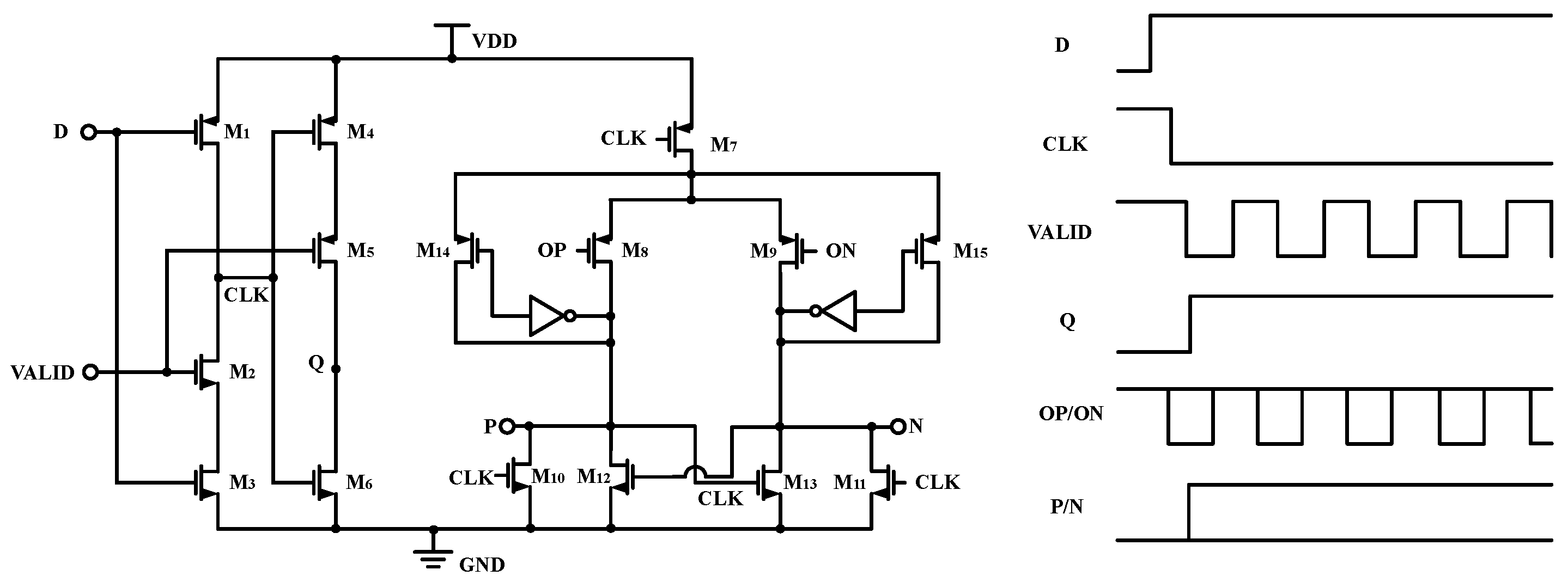
3.2. Sample-Data Isolation Based SAR ADC
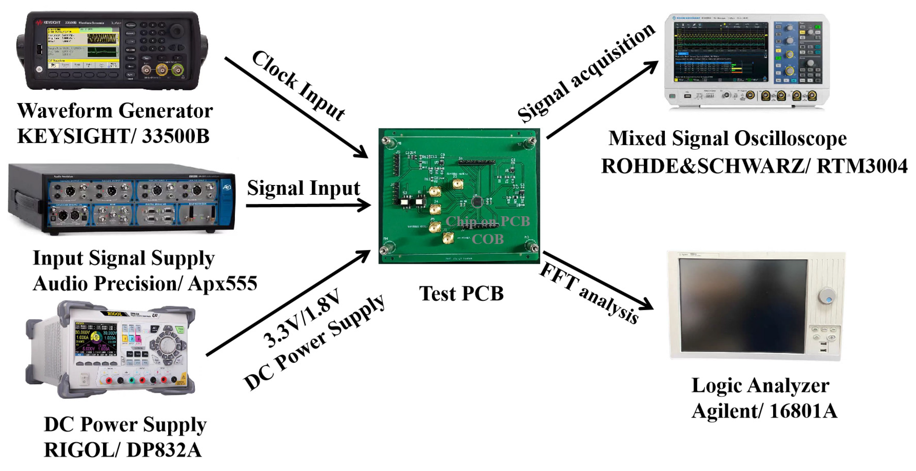
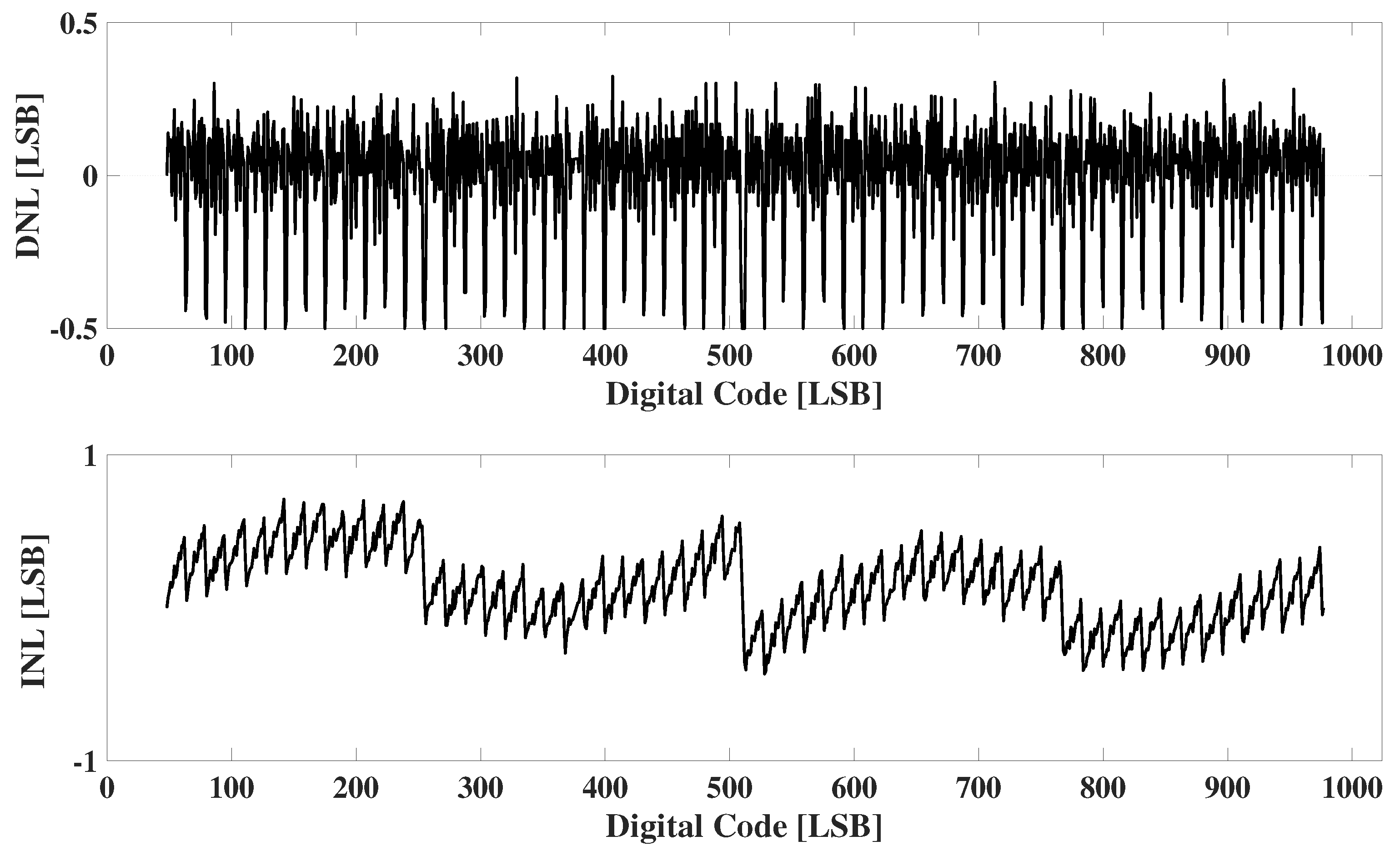
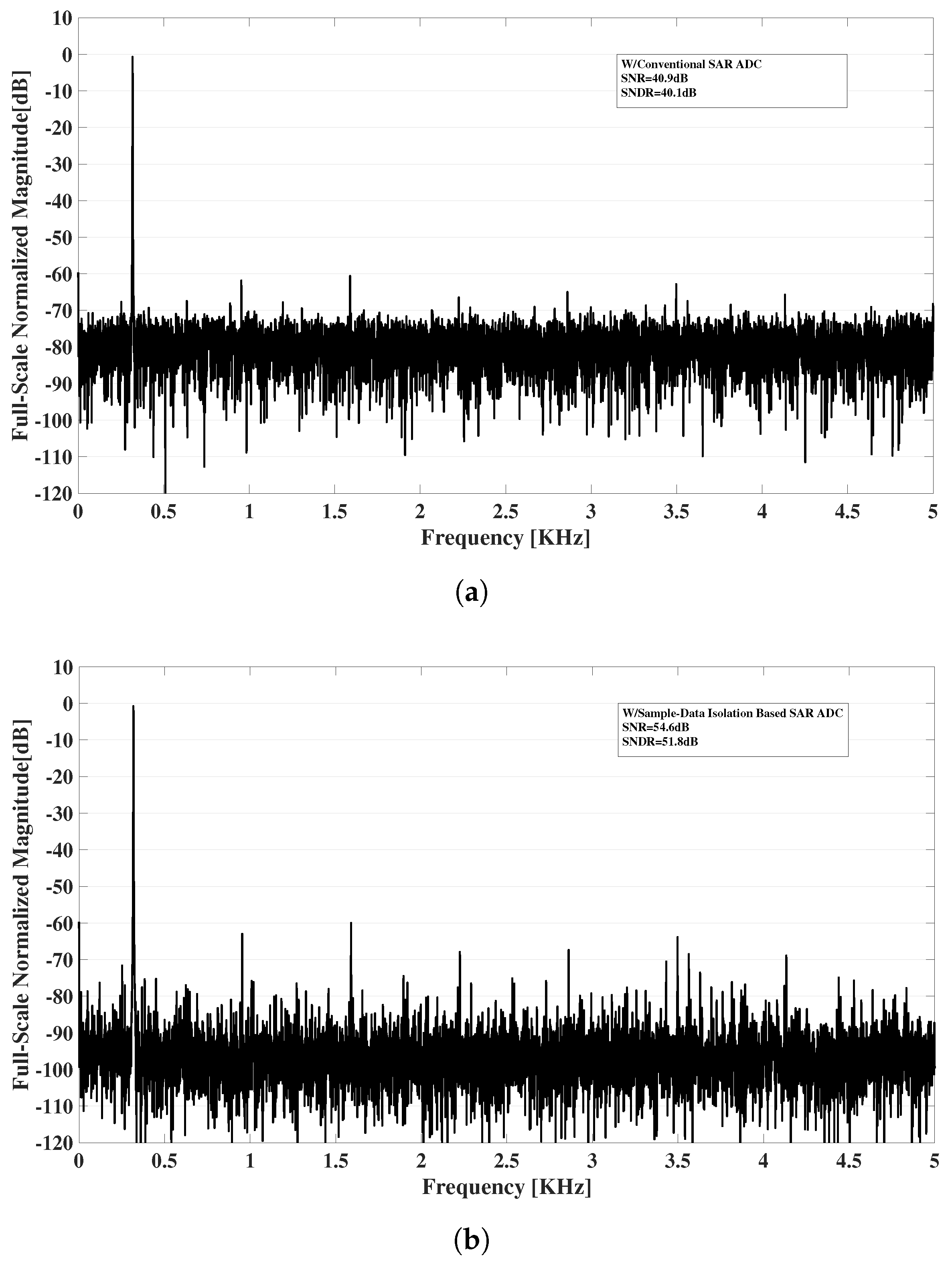
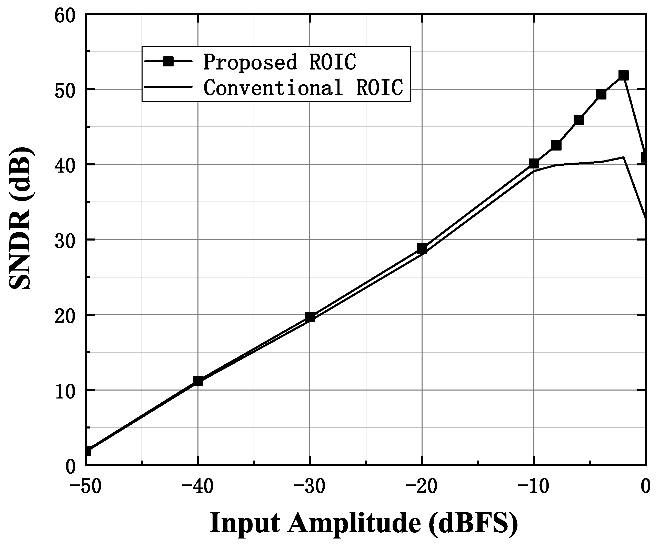
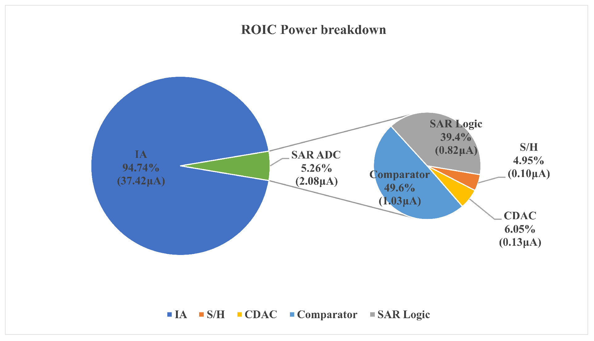
4. Measurement Results
5. Conclusions
Author Contributions
Funding
Institutional Review Board Statement
Informed Consent Statement
Data Availability Statement
Acknowledgments
Conflicts of Interest
References
- Eide, P.K.; Sorteberg, A.; Meling, T.R.; Sorteberg, W. Baseline pressure errors (BPEs) extensively influence intracranial pressure scores: Results of a prospective observational study. BioMed. Eng. OnLine 2014, 13, 1–16. [Google Scholar] [CrossRef]
- Eide, P.K.; Due-Tønnessen, B.; Helseth, E.; Lundar, T. Differences in quantitative characteristics of intracranial pressure in hydrocephalic children treated surgically or conservatively. Pediatr. Neurosurg. 2002, 36, 304–313. [Google Scholar] [CrossRef] [PubMed]
- Pedersen, S.H.; Lilja-Cyron, A.; Andresen, M.; Juhler, M. The relationship between intracranial pressure and age-chasing age-related reference values. World Neurosurg. 2018, 110, 119–123. [Google Scholar] [CrossRef]
- Washko, F.M.; Edwards, W.S.; Washko, L.A. Development of a Smart Cervical Collar System for Feedback Control of Intracranial Pressure after Traumatic Head Injury. In Proceedings of the 2021 Seventh International conference on Bio Signals, Images, and Instrumentation (ICBSII), Chennai, India, 25–27 March 2021; pp. 1–6. [Google Scholar]
- Jahangir, A.; Tirdad, K.; Dela Cruz, A.; Sadeghian, A.; Cusimano, M. An Application of Machine Learning to Forecast Hypertension Signals in Intracranial Pressure: A Comparison of Various Algorithms. IEEE Syst. Man Cybern. Mag. 2022, 8, 29–38. [Google Scholar] [CrossRef]
- Andrade, R.A.P.; Oshiro, H.E.; Miyazaki, C.K.; Hayashi, C.Y.; de Morais, M.A.; Brunelli, R.; Carmo, J.P. A Nanometer Resolution Wearable Wireless Medical Device for Non Invasive Intracranial Pressure Monitoring. IEEE Sens. J. 2021, 21, 22270–22284. [Google Scholar] [CrossRef]
- Wu, Z.; Jiang, H.; Guo, Y.; Zhang, C.; Jia, W.; Wang, Z. Wireless intracranial pressure monitoring system based on an air pressure sensor. In Proceedings of the 2017 IEEE Biomedical Circuits and Systems Conference (BioCAS), Turin, Italy, 19–21 October 2017; pp. 1–4. [Google Scholar]
- Jiang, H.; Guo, Y.; Wu, Z.; Zhang, C.; Jia, W.; Wang, Z. Implantable Wireless Intracranial Pressure Monitoring Based on Air Pressure Sensing. IEEE Trans. Biomed. Circuits Syst. 2018, 12, 1076–1087. [Google Scholar] [CrossRef] [PubMed]
- Liu, T.; Yao, P.; Li, Z.; Feng, H.; Zhuang, C.; Sun, X.; Liu, C.; Xue, N. Implantable Sufficiently Integrated Multimodal Flexible Sensor for Intracranial Monitoring. In Proceedings of the 2021 IEEE Sensors, Sydney, Australia, 31 October–3 November 2021; pp. 1–4. [Google Scholar]
- Harika, P.B.; Kundu, S. Design of MEMS-Based Piezoresistive Pressure Sensor Using Two Concentric Wheatstone bridge Circuits for Intracranial Pressure Measurement. In Proceedings of the 2022 IEEE International Conference of Electron Devices Society Kolkata Chapter (EDKCON), Kolkata, India, 26–27 November 2022; pp. 380–385. [Google Scholar]
- Harary, M.; Dolmans, R.G.; Gormley, W.B. Intracranial pressure monitoring—Review and avenues for development. Sensors 2018, 18, 465. [Google Scholar] [CrossRef]
- Topalli, G.; Fan, Y.; Cheung, M.Y.; Veeraraghavan, A.; Hirzallah, M.; Chi, T. 17.11 A 9mW Ultrasonic Through Transmission Transceiver for Non-Invasive Intracranial Pressure Sensing. In Proceedings of the 2024 IEEE International Solid-State Circuits Conference (ISSCC), San Francisco, CA, USA, 18–22 February 2024; pp. 334–336. [Google Scholar]
- Raghunathan, A.; Antony, J.K. MEMS based intracranial pressure monitoring sensor. In Proceedings of the 2017 2nd IEEE International Conference on Recent Trends in Electronics, Information & Communication Technology (RTEICT), Bangalore, India, 19–20 May 2017; pp. 451–456. [Google Scholar]
- Meng, T.; Jin, Y. The Schemes for Reducing Temperature Drift in Intracranial Pressure Monitoring Sensor with half-bridge Pressure Transducer. In Proceedings of the 2023 16th International Congress on Image and Signal Processing, BioMedical Engineering and Informatics (CISP-BMEI), Taizhou, China, 28–30 October 2023; pp. 1–6. [Google Scholar]
- Maruyama, M.; Taguchi, S.; Yamanoue, M.; Iizuka, K. An Analog Front-End for a Multifunction Sensor Employing a Weak-Inversion Biasing Technique with 26 nVrms, 25 aCrms, and 19 fArms Input-Referred Noise. IEEE J. Solid-State Circuits 2016, 51, 2252–2261. [Google Scholar] [CrossRef]
- Ghanbari, M.M.; Tsai, J.M.; Nirmalathas, A.; Muller, R.; Gambini, S. An Energy-Efficient Miniaturized Intracranial Pressure Monitoring System. IEEE J. Solid-State Circuits 2017, 52, 720–734. [Google Scholar] [CrossRef]
- Kosuge, A.; Hamada, M.; Kuroda, T. A 6-Gb/s Inductively-Powered Non-Contact Connector With Rotatable Transmission Line Coupler and Interface Bridge IC. IEEE J. Solid-State Circuits 2022, 57, 535–545. [Google Scholar] [CrossRef]
- Jiang, H.; Makinwa, K.A.A. Energy-efficient bridge-to-digital converters. In Proceedings of the 2018 IEEE Custom Integrated Circuits Conference (CICC), San Diego, CA, USA, 8–11 April 2018; pp. 1–7. [Google Scholar]
- Rezvanitabar, A.; Jung, G.; Degertekin, F.L.; Ghovanloo, M. Toward an Energy-Efficient Bridge-to-Digital Intracranial Pressure Sensing Interface. In Proceedings of the 2018 IEEE Biomedical Circuits and Systems Conference (BioCAS), Cleveland, OH, USA, 17–19 October 2018; pp. 1–4. [Google Scholar]
- Besirli, M.; Ture, K.; Barrettino, D.; Beghetti, M.; Mattavelli, M.; Dehollain, C.; Maloberti, F. A 0.4 nJ Excitation Energy Bridge-to-Digital Converter for Implantable Pulmonary Artery Pressure Monitoring. In Proceedings of the 2021 IEEE Biomedical Circuits and Systems Conference (BioCAS), Berlin, Germany, 7–9 October 2021; pp. 1–4. [Google Scholar]
- Besirli, M.; Ture, K.; Beghetti, M.; Dehollain, C.; Mattavelli, M.; Maloberti, F.; Barrettino, D. An Energy-Efficient Bridge-to-Digital Converter for Implantable Pressure Monitoring Systems. IEEE Trans. Biomed. Circuits Syst. 2022, 16, 732–741. [Google Scholar] [CrossRef] [PubMed]
- Zhang, S.; Zhou, X.; Gao, C.; Li, Q. A 130-dB CMRR Instrumentation Amplifier With Common-Mode Replication. IEEE J. Solid-State Circuits 2022, 57, 278–289. [Google Scholar] [CrossRef]
- Fang, L.; Gui, P. A Low-Noise Low-Power Chopper Instrumentation Amplifier with Robust Technique for Mitigating Chopping Ripples. IEEE J. Solid-State Circuits 2022, 57, 1800–1811. [Google Scholar] [CrossRef]
- Zheng, J.; Ki, W.H.; Hu, L.; Tsui, C.Y. Chopper capacitively coupled instrumentation amplifier capable of handling large electrode offset for biopotential recordings. IEEE Trans. Circuits Syst. II Express Briefs 2017, 64, 1392–1396. [Google Scholar] [CrossRef]
- Ha, H.; Van Hoof, C.; Van Helleputte, N. Measurement and Analysis of Input-Signal Dependent Flicker Noise Modulation in Chopper Stabilized Instrumentation Amplifier. IEEE Solid-State Circuits Lett. 2018, 1, 90–93. [Google Scholar] [CrossRef]
- An, J.-S.; Ra, J.-H.; Kang, E.; Pertijs, M.A.P.; Han, S.-H. A Readout IC for Capacitive Touch Screen Panels with 33.9 dB Charge-Overflow Reduction Using Amplitude-Modulated Multi-Frequency Excitation. IEEE J. Solid-State Circuits 2021, 56, 3486–3498. [Google Scholar] [CrossRef]
- Huang, X.; Londoño-Ramírez, H.; Ballini, M.; Van Hoof, C.; Genoe, J.; Haesler, S.; Gielen, G.; Helleputte, N.V.; Lopez, C. Actively Multiplexed μ ECoG Brain Implant System with Incremental-ΔΣ ADCs Employing Bulk-DACs. IEEE J. Solid-State Circuits 2022, 57, 3312–3323. [Google Scholar] [CrossRef]
- Park, S.-H.; Kim, H.-S.; Bang, J.-S.; Cho, G.-H.; Cho, G.-H. A 0.26-nJ/node, 400-kHz Tx Driving, Filtered Fully Differential Readout IC With Parasitic RC Time Delay Reduction Technique for 65-in 169 × 97 Capacitive-Type Touch Screen Panel. IEEE J. Solid-State Circuits 2017, 52, 528–542. [Google Scholar] [CrossRef]
- Xu, Y.; Hu, H.; Muhlestein, J.; Moon, U.-K. A 77-dB-DR 0.65-mW 20-MHz 5th-Order Coupled Source Followers Based Low-Pass Filter. IEEE J. Solid-State Circuits 2020, 55, 2810–2818. [Google Scholar] [CrossRef]
- Lin, F.; Mak, P.-I.; Martins, R.P. An RF-to-BB-Current-Reuse Wideband Receiver with Parallel N-Path Active/Passive Mixers and a Single-MOS Pole-Zero LPF. IEEE J. Solid-State Circuits 2014, 49, 2547–2559. [Google Scholar] [CrossRef]
- Song, P.; Hashemi, H. mm-Wave Mixer-First Receiver with Selective Passive Wideband Low-Pass Filtering. IEEE J. Solid-State Circuits 2021, 56, 1454–1463. [Google Scholar] [CrossRef]
- Malki, B.; Verbruggen, B.; Martens, E.; Wambacq, P.; Craninckx, J. A 150 kHz–80 MHz BW Discrete-Time Analog Baseband for Software-Defined-Radio Receivers using a 5th-Order IIR LPF, Active FIR and a 10 bit 300 MS/s ADC in 28 nm CMOS. IEEE J. Solid-State Circuits 2016, 51, 1593–1606. [Google Scholar] [CrossRef]
- Lee, J.; Lee, K.-R.; Ha, U.; Kim, J.-H.; Lee, K.; Gweon, S.; Jang, J.; Yoo, H.-J. A 0.8-V 82.9- μ W In-Ear BCI Controller IC With 8.8 PEF EEG Instrumentation Amplifier and Wireless BAN Transceiver. IEEE J. Solid-State Circuits 2019, 54, 1185–1195. [Google Scholar] [CrossRef]
- Park, J.H.; Tang, T.; Zhang, L.; Ng, K.A.; Gammad, G.G.L.; Yen, S.-C.; Yoo, J. A 15-Channel Orthogonal Code Chopping Instrumentation Amplifier for Area-Efficient, Low-Mismatch Bio-Signal Acquisition. IEEE J. Solid-State Circuits 2020, 55, 2771–2780. [Google Scholar] [CrossRef]
- Ahmad, M.; Malik, S.; Dewan, S.; Bose, A.K.; Maddipatla, D.; Narakathu, B.B.; Atashbar, M.Z.; Baghini, M.S. An Auto-Calibrated Resistive Measurement System with Low Noise Instrumentation ASIC. IEEE J. Solid-State Circuits 2020, 55, 3036–3050. [Google Scholar] [CrossRef]
- Qu, T.; Pan, Q.; Liu, L.; Zeng, X.; Hong, Z.; Xu, J. A 1.8-GΩ Input-Impedance 0.15–μV Input-Referred–Ripple Chopper Amplifier with Local Positive Feedback and SAR-Assisted Ripple Reduction. IEEE J. Solid-State Circuits 2023, 58, 796–805. [Google Scholar] [CrossRef]
- Wu, R.; Huijsing, J.H.; Makinwa, K.A.A. A 21b ±40 mV range read-out IC for bridge transducers. In Proceedings of the 2011 IEEE International Solid-State Circuits Conference, San Francisco, CA, USA, 20–24 February 2011; pp. 110–112. [Google Scholar]
- Xu, W.; Li, Z.; Fang, Z.; Wang, B.; Hong, L.; Yang, G.; Han, S.-T.; Zhao, X.; Wang, X. A Sub-5mW Monolithic CMOS-MEMS Thermal Flow Sensing SoC with ±6 m/s Linear Range. IEEE J. Solid-State Circuits 2024, 59, 1486–1496. [Google Scholar] [CrossRef]
- Park, Y.; Cha, J.-H.; Han, S.-H.; Park, J.-H.; Kim, S.-J. A 3.8-μW 1.5-NEF 15-GΩ Total Input Impedance Chopper Stabilized Amplifier With Auto-Calibrated Dual Positive Feedback in 110-nm CMOS. IEEE J. Solid-State Circuits 2022, 57, 2449–2461. [Google Scholar] [CrossRef]
- Jiang, H.; Nihtianov, S.; Makinwa, K.A.A. An Energy-Efficient 3.7-nV/ √ Hz Bridge Readout IC with a Stable Bridge Offset Compensation Scheme. IEEE J. Solid-State Circuits 2019, 54, 856–864. [Google Scholar] [CrossRef]
- Donida, A.; Di Dato, G.; Cunzolo, P.; Sala, M.; Piffaretti, F.; Orsatti, P.; Barrettino, D. 21.7 A 0.036mbar circadian and cardiac intraocular pressure sensor for smart implantable lens. In Proceedings of the 2015 IEEE International Solid-State Circuits Conference—(ISSCC) Digest of Technical Papers, San Francisco, CA, USA, 22–26 February 2015; pp. 1–3. [Google Scholar]
- Jiang, H.; Makinwa, K.A.A.Č.; Nihitanov, S. An energy-efficient readout method for piezoresistive differential pressure sensors. In Proceedings of the IECON 2017—43rd Annual Conference of the IEEE Industrial Electronics Society, Beijing, China, 29 October–1 November 2017; pp. 4287–4291. [Google Scholar]
- Harrison, R.R.; Charles, C. A low-power low-noise CMOS amplifier for neural recording applications. IEEE J. Solid-State Circuits 2003, 38, 958–965. [Google Scholar] [CrossRef]
- Zhan, M.; Jie, L.; Zhong, Y.; Sun, N. A 10-mW 10-ENoB 1-GS/s Ring-Amp-Based Pipelined TI-SAR ADC with Split MDAC and Switched Reference Decoupling Capacitor. IEEE J. Solid-State Circuits 2023, 58, 3576–3585. [Google Scholar] [CrossRef]
- Guo, Y.; Jin, J.; Liu, X.; Zhou, J. A 60-MS/s 5-MHz BW Noise-Shaping SAR ADC with Integrated Input Buffer Achieving 84.2-dB SNDR and 97.3-dB SFDR Using Dynamic Level-Shifting and ISI-Error Correction. IEEE J. Solid-State Circuits 2023, 58, 474–485. [Google Scholar] [CrossRef]
- Guo, X.; Li, H.; Chen, Y. A 3.58 nJ/Node Dual Cross Correlation Analog-Front-End Circuit with ADC for Mutual Capacitive Panel. IEEE J. Solid-State Circuits 2024, 59, 282–293. [Google Scholar] [CrossRef]
- Choi, S.; Ku, H.-S.; Son, H.; Kim, B.; Park, H.-J.; Sim, J.-Y. An 84.6-dB-SNDR and 98.2-dB-SFDR Residue-Integrated SAR ADC for Low-Power Sensor Applications. IEEE J. Solid-State Circuits 2018, 53, 404–417. [Google Scholar] [CrossRef]


| Technology | Accuracy | Power Consumption | Size | Complexity | Long-Term Stability |
|---|---|---|---|---|---|
| Strain Gauges | Moderate | Low | Large | Low | Poor |
| Fiber Optic Sensors | High | Moderate | Medium | High | Excellent |
| Piezoresistive Sensors | High | High | Small | Moderate | Moderate |
| Parameter | This Work | [37] | [40] | [41] | [42] |
|---|---|---|---|---|---|
| Architecture | IA+SAR | CFIA+DTΔΣM | CCIA+CTΔΣM | IA+SAR | RC+CTΔΣM |
| Process (nm) | 180 | 700 | 180 | 350 | 350 |
| Supply (V) | 1.8 | 5 | 1.8 | 3.3 | 5 |
| Power (mW) | 0.071 | 1.35 | 2.16 | 0.201 | 4.3 |
| Area (mm2) | 1.35 | 6 | 0.73 | 2 | / |
| BW (kHz) | 200 | 0.004 | 1 | 200 | 2 |
| SNR/SNDR (dB) | 54.6/51.8 | 91.2 */- | -/88 * | -/50 | 80/- |
| FoMSNR (dB) | 149.1(@32×) | 125.9 *(@100×) | - | - | 136.7(@32×) |
| FoMSNDR (dB) | 146.3(@32×) | - | 144.7 *(@100×) | 139.9(@178×) | - |
Disclaimer/Publisher’s Note: The statements, opinions and data contained in all publications are solely those of the individual author(s) and contributor(s) and not of MDPI and/or the editor(s). MDPI and/or the editor(s) disclaim responsibility for any injury to people or property resulting from any ideas, methods, instructions or products referred to in the content. |
© 2025 by the authors. Licensee MDPI, Basel, Switzerland. This article is an open access article distributed under the terms and conditions of the Creative Commons Attribution (CC BY) license (https://creativecommons.org/licenses/by/4.0/).
Share and Cite
Yao, S.; Shan, Q.; Xiao, J.; Wei, Z.; Huang, S. Enhanced Linearity in Intracranial Pressure Monitoring System Through Sample Isolation Bridge ROIC. Appl. Sci. 2025, 15, 3008. https://doi.org/10.3390/app15063008
Yao S, Shan Q, Xiao J, Wei Z, Huang S. Enhanced Linearity in Intracranial Pressure Monitoring System Through Sample Isolation Bridge ROIC. Applied Sciences. 2025; 15(6):3008. https://doi.org/10.3390/app15063008
Chicago/Turabian StyleYao, Shaopeng, Qiang Shan, Jinjin Xiao, Zihui Wei, and Shuilong Huang. 2025. "Enhanced Linearity in Intracranial Pressure Monitoring System Through Sample Isolation Bridge ROIC" Applied Sciences 15, no. 6: 3008. https://doi.org/10.3390/app15063008
APA StyleYao, S., Shan, Q., Xiao, J., Wei, Z., & Huang, S. (2025). Enhanced Linearity in Intracranial Pressure Monitoring System Through Sample Isolation Bridge ROIC. Applied Sciences, 15(6), 3008. https://doi.org/10.3390/app15063008