
Enhancing Security and Efficiency in IoT Assistive Technologies: A Novel Hybrid Systolic Array Multiplier for Cryptographic Algorithms


Abstract
1. Introduction
1.1. Literature Review
1.2. Paper Contribution
1.3. Paper Organization
2. Exploring Dickson Basis Multiplication in GF()
3. Dependency Graph
4. Derivation of the Hybrid Compact Systolic Multiplier
4.1. Scheduling Function
4.2. Projection Function
4.3. The Explored Multiplier Layout
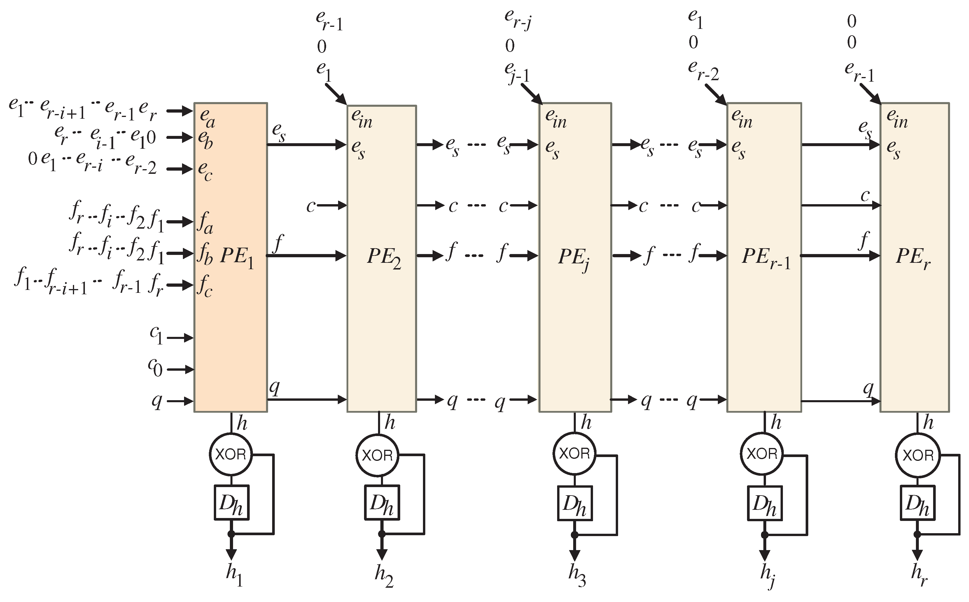
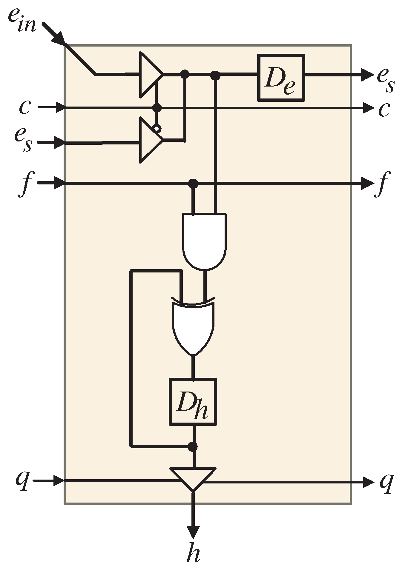
- In the initial clock period, the latches are reset to zero (), ensuring that the input bits of , for j ranging from 1 to r, are initialized appropriately at the inputs of the XOR gates located both within and outside each processing element. This initialization is critical for maintaining data integrity, as depicted in Figure 3, Figure 4 and Figure 5. Concurrently, the control signal c is activated (), allowing the input signals to pass through the input port of the regular PEs (), where j is within the range from 1 to r. This enables the utilization of these signals within each processing element. Additionally, during this clock period, control signals and are deactivated ( and ), permitting the first bits of the and signals, for i ranging from 1 to r, to traverse the input ports and of the first PE ().
- From the second clock period up to the clock period, control signal c is deactivated (), allowing the sequential passage of signals through the input port of the regular PEs (). This step is essential for their effective use within each processing element. During this interval, control signals and remain deactivated ( and ), facilitating the passage of all remaining sequential bits of the and signals through the input ports and of the first PE (), thereby ensuring their availability for processing.
- Upon completing the first r clock cycles, control signal q is activated (), enabling the transfer of the intermediate bits of h to the accumulator, which comprises XOR gates and latches positioned at the output of each PE, as illustrated in Figure 3. These accumulated bits are stored in the latches and are intended to be combined with the output bits generated after the next set of r clock cycles, marking the beginning of the second operational phase of the systolic array.
- Following the completion of the first r clock cycles, the systolic array transitions into a second computation phase. At the first clock cycle of this phase, the latches within each PE are reset to initialize the input bits of , for j ranging from 1 to r, to zero at the inputs of the XOR gates, as shown in Figure 4 and Figure 5. Simultaneously, control signal c is activated () to facilitate the utilization of zero input signals assigned to input port within each regular PE (). During this clock period, control signals and are set to 1 and 0, respectively ( and ), allowing the first bits of the and signals, for i ranging from 1 to r, to pass through the input ports and of the first PE ().
- From the second clock period until the clock period of the second computation phase, control signal c is deactivated (), enabling the sequential passage of signals through the input port of the regular PEs (). This allows for their effective use within each processing element. During this period, control signals and maintain their states ( and ), ensuring that all remaining sequential bits of the and signals pass through the input ports and .
- At the conclusion of the second r clock cycles, control signal q is activated () to transfer the intermediate bits of h to the accumulator (XOR gates and latches) located at the output of each PE, as shown in Figure 3. These bits are added to the previously stored output bits from the first computation phase. The accumulated bits are retained in the latches for subsequent addition to the next output bits produced after the third r clock cycles, marking the beginning of the third operational phase of the systolic array.
- After the second r clock cycles, the systolic array enters the third computation phase. At the first clock cycle of this phase, the latches within each PE are reset to initialize the input bits of , for j ranging from 1 to r, to zero at the inputs of the XOR gates inside each PE, as shown in Figure 4 and Figure 5. Concurrently, control signal c is activated () to facilitate the use of the input signals , for j ranging from 1 to r, assigned to input port within each regular PE (). Furthermore, during this clock period, control signals and are both activated ( and ), allowing the first bits of the and signals, for i ranging from 1 to r, to pass through the input ports and of the first PE ().
- From the second clock period until the clock period of the third computation phase, control signal c is deactivated (), facilitating the sequential passage of the signals , for i ranging from 1 to r, through the input port , thereby allowing their effective use within each of the regular PEs (). During these clock periods, control signals and retain their states ( and ), enabling all remaining sequential bits of the and signals, for i ranging from 1 to r, to traverse the input ports and , respectively. This ensures their availability for processing throughout these clock cycles.
- At the conclusion of the third computation phase, control signal q is activated () to facilitate the transfer of the resulting intermediate bits of h to the accumulator (XOR gates and latches) located at the output of each PE, as depicted in Figure 3. The obtained bits are added to the output bits previously stored in the latches following the second computation phase. The output bits from the third computation phase will likewise be stored in the latches, culminating in the final computation result of the hybrid systolic multiplier.
5. Findings and Analysis
5.1. Complexity Examination
5.2. Implementation Insights and Results
6. Findings Overview and Conclusions
Author Contributions
Funding
Institutional Review Board Statement
Informed Consent Statement
Data Availability Statement
Acknowledgments
Conflicts of Interest
Abbreviations
| IoT | Internet of Things |
| TLS | Transport Layer Security |
| PKI | Public Key Infrastructure |
| PB | Polynomial Basis |
| NB | Normal Basis |
| DB | Dual Basis |
| RB | Redundant Basis |
| PE | Processing Element |
| ADP | Area-Delay Product |
| PDP | Power-Delay Product |
| ASIC | Application Specific Integrated Circuit |
| ECC | Elliptic Curve Cryptography |
| DG | Dependency Graph |
| AOP | All-One Polynomial |
| VLSI | Very Large Scale Integrated Circuit |
| CPD | Critical Path Delay |
References
- Ahmmed, Z.N.; Kheder, M.Q. Enhancing Mobility With IOT-based Autonomous Wheelchair. Sci. J. Univ. Zakho 2024, 12, 497–504. [Google Scholar] [CrossRef]
- Zhang, Z.; Xu, P.; Wu, C.; Yu, H. Smart Nursing Wheelchairs: A New Trend in Assisted Care and the Future of Multifunctional Integration. Biomimetics 2024, 9, 492. [Google Scholar] [CrossRef] [PubMed]
- Nasabeh, S.S.; Meliá, S. Enhancing quality of life for the hearing-impaired: A holistic approach through the MoSIoT framework. In Universal Access in the Information Society; Springer: Berlin/Heidelberg, Germany, 2024; pp. 1–23. [Google Scholar]
- Lin, C.H.; Li, Y.L.; Ciou, W.S.; Du, Y.C. An IoT-enabled EEG headphones with customized music for chronic tinnitus assessment and symptom management. Internet Things 2024, 28, 101411. [Google Scholar]
- Ibrahim, A.K.; Hassan, M.M.; Ali, I.A. Smart Homes for Disabled People: A Review Study. Sci. J. Univ. Zakho 2022, 10, 213–221. [Google Scholar] [CrossRef]
- Krishnamoorthy, S.; Dua, A.; Gupta, S. Role of emerging technologies in future IoT-driven Healthcare 4.0 technologies: A survey, current challenges and future directions. J. Ambient Intell. Humaniz. Comput. 2023, 14, 361–407. [Google Scholar] [CrossRef]
- Sripathi, M.; Leelavati, T. The Fourth Industrial Revolution: A paradigm shift in healthcare delivery and management. In Digital Transformation in Healthcare 5.0: Volume 1: IoT, AI and Digital Twin; De Gruyter: Berlin, Germany, 2024; p. 67. [Google Scholar]
- Murugan, T.; Jaisingh, W.; Varalakshmi, P. Technologies for Sustainable Healthcare Development; IGI Global: Hershey, PA, USA, 2024. [Google Scholar]
- Zhang, R.; Zhou, Y.; Zhang, J.; Zhao, J. Cloud-integrated robotics: Transforming healthcare and rehabilitation for individuals with disabilities. Proc. Indian Natl. Sci. Acad. 2024, 90, 752–763. [Google Scholar] [CrossRef]
- Adeghe, E.P.; Okolo, C.A.; Ojeyinka, O.T. A review of emerging trends in telemedicine: Healthcare delivery transformations. Int. J. Life Sci. Res. Arch. 2024, 6, 137–147. [Google Scholar] [CrossRef]
- Vrančić, A.; Zadravec, H.; Orehovački, T. The Role of Smart Homes in Providing Care for Older Adults: A Systematic Literature Review from 2010 to 2023. Smart Cities 2024, 7, 1502–1550. [Google Scholar] [CrossRef]
- Valero, C.; Pérez, J.; Solera-Cotanilla, S.; Vega-Barbas, M.; Suarez-Tangil, G.; Alvarez-Campana, M.; López, G. Analysis of security and data control in smart personal assistants from the user’s perspective. Future Gener. Comput. Syst. 2023, 144, 12–23. [Google Scholar] [CrossRef]
- Sivakumar, C.; Mone, V.; Abdumukhtor, R. Addressing privacy concerns with wearable health monitoring technology. Wiley Interdiscip. Rev. Data Min. Knowl. Discov. 2024, 14, e1535. [Google Scholar] [CrossRef]
- Nissar, G.; Khan, R.A.; Mushtaq, S.; Lone, S.A.; Moon, A.H. IoT in healthcare: A review of services, applications, key technologies, security concerns, and emerging trends. Multimed. Tools Appl. 2024, 83, 80283. [Google Scholar] [CrossRef]
- Marchang, J.; Di Nuovo, A. Assistive multimodal robotic system (AMRSys): Security and privacy issues, challenges, and possible solutions. Appl. Sci. 2022, 12, 2174. [Google Scholar] [CrossRef]
- Ahmed, S.F.; Alam, M.S.B.; Afrin, S.; Rafa, S.J.; Rafa, N.; Gandomi, A.H. Insights into Internet of Medical Things (IoMT): Data fusion, security issues and potential solutions. Inf. Fusion 2024, 102, 102060. [Google Scholar] [CrossRef]
- Bernal, S.L.; Celdrán, A.H.; Pérez, G.M.; Barros, M.T.; Balasubramaniam, S. Cybersecurity in brain-computer interfaces: State-of-the-art, opportunities, and future challenges. arXiv 2019, arXiv:1908.03536. [Google Scholar]
- Hasan, A.; Negre, C. Low space complexity multiplication over binary fields with Dickson polynomial representation. IEEE Trans. Comput. 2010, 60, 602–607. [Google Scholar] [CrossRef]
- Chiou, C.W.; Lee, C.M.; Sun, Y.S.; Lee, C.Y.; Lin, J.M. High-throughput Dickson basis multiplier with a trinomial for lightweight cryptosystems. IET Comput. Digit. Tech. 2018, 12, 187–191. [Google Scholar] [CrossRef]
- Chiou, C.; Sun, Y.S.; Lee, C.M.; Liou, J.Y. Low-complexity unidirectional systolic Dickson basis multiplier for lightweight cryptosystems. Electron. Lett. 2019, 55, 28–30. [Google Scholar] [CrossRef]
- Pillutla, S.R.; Boppana, L. Area-efficient low-latency polynomial basis finite field GF(2m) systolic multiplier for a class of trinomials. Microelectron. J. 2020, 97, 104709. [Google Scholar] [CrossRef]
- Imana, J.L. LFSR-Based Bit-Serial GF(2m) Multipliers Using Irreducible Trinomials. IEEE Trans. Comput. 2020, 70, 156–162. [Google Scholar]
- Pillutla, S.R.; Boppana, L. Low-latency area-efficient systolic bit-parallel GF(2m) multiplier for a narrow class of trinomials. Microelectron. J. 2021, 117, 105275. [Google Scholar] [CrossRef]
- Li, Y.; Cui, X.; Zhang, Y. An Efficient CRT-based Bit-parallel Multiplier for Special Pentanomials. IEEE Trans. Comput. 2021, 71, 736–742. [Google Scholar] [CrossRef]
- Li, Y.; Zhang, Y.; He, W. Fast hybrid Karatsuba multiplier for type II pentanomials. IEEE Trans. Very Large Scale Integr. (VLSI) Syst. 2020, 28, 2459–2463. [Google Scholar] [CrossRef]
- Meher, P.K.; Lou, X. Low-Latency, Low-Area, and Scalable Systolic-Like Modular Multipliers for GF(2m) Based on Irreducible All-One Polynomials. IEEE Trans. Circuits Syst. I Regul. Pap. 2016, 64, 399–408. [Google Scholar] [CrossRef]
- Mohaghegh, S.; Yemiscoglu, G.; Muhtaroglu, A. Low-Power and Area-Efficient Finite Field Multiplier Architecture Based on Irreducible All-One Polynomials. In Proceedings of the 2020 IEEE International Symposium on Circuits and Systems (ISCAS), Virtual, 10–21 October 2020; pp. 1–5. [Google Scholar]
- Zhang, Y.; Li, Y. Efficient Hybrid GF(2m) Multiplier for All-One Polynomial Using Varied Karatsuba Algorithm. IEICE Trans. Fundam. Electron. Comput. Sci. 2021, 104, 636–639. [Google Scholar] [CrossRef]
- Chiou, C.W.; Lee, C.Y.; Deng, A.W.; Lin, J.M. Concurrent error detection in Montgomery multiplication over GF(2m). IEICE Trans. Fundam. Electron. Commun. Comput. Sci. 2006, E89-A, 566–574. [Google Scholar] [CrossRef]
- Zhou, B.B. A New Bit Serial Systolic Multiplier over GF(2m). IEEE Trans. Comput. 1988, 37, 749–751. [Google Scholar] [CrossRef]
- Fenn, S.T.J.; Taylor, D.; Benaissa, M. A Dual Basis Bit Serial Systolic Multiplier for GF(2m). Integr. VLSI J. 1995, 18, 139–149. [Google Scholar] [CrossRef]
- Kim, K.W.; Jeon, J.C. Polynomial Basis Multiplier Using Cellular Systolic Architecture. IETE J. Res. 2014, 60, 194–199. [Google Scholar] [CrossRef]
- Choi, S.; Lee, K. Efficient systolic modular multiplier/squarer for fast exponentiation over GF(2m). IEICE Electron. Express 2015, 12, 20150222. [Google Scholar] [CrossRef]
- Kim, K.W.; Jeon, J.C. A semi-systolic Montgomery multiplier over GF(2m). IEICE Electron. Express 2015, 12, 20150769. [Google Scholar] [CrossRef]
- Lee, C.Y.; Lu, E.H.; Lee, J.Y. Bit-Parallel Systolic Multipliers for GF(2m) Fields Defined by All-One and Equally-Spaced Polynomials. IEEE Trans. Comput. 2001, 50, 358–393. [Google Scholar]
- Lee, C.Y.; Lu, E.H.; Sun, L.F. Low-Complexity Bit-Parallel Systolic Architecture for Computing AB2 + C in a Class of Finite Field GF(2m). IEEE Trans. Circuits Syst. II 2001, 50, 519–523. [Google Scholar]
- Lee, C.Y.; Chiou, C.W. Efficient Design of Low-Complexity Bit-Parallel Systolic Hankel Multipliers to Implement Multiplication in Normal and Dual Bases of GF(2m). IEICE Trans. Fundam. Electron. Commun. Comput. Sci. 2005, E88-A, 3169–3179. [Google Scholar] [CrossRef]
- Lee, C.Y. Low-latency bit-pararallel systolic multiplier for irreducible xm + xn + 1 with GCD(m,n) = 1. IEICE Trans. Fundam. Electron. Commun. Comput. Sci. 2008, 55, 828–837. [Google Scholar]
- Bayat-Sarmadi, S.; Farmani, M. High-Throughput Low-Complexity Systolic Montgomery Multiplication Over GF(2m) Based on Trinomials. IEEE Trans. Circuits Syst. II 2015, 62, 377–381. [Google Scholar]
- Mathe, S.E.; Boppana, L. Bit-parallel systolic multiplier over GF(2m) for irreducible trinomials with ASIC and FPGA implementations. IET Circuits Desvices Syst. 2018, 12, 315–325. [Google Scholar] [CrossRef]
- Lee, C.Y.; Chiou, C.W.; Lin, J.M. Concurrent error detection in a polynomial basis multiplier over GF(2m). J. Electron. Test. 2006, 22, 143–150. [Google Scholar] [CrossRef]
- Huang, W.T.; Chang, C.H.; Chiou, C.W.; Chou, F.H. Concurrent error detection and correction in a polynomial basis multiplier over GF(2m). IET Inf. Secur. 2010, 4, 111–124. [Google Scholar] [CrossRef]
- Lee, K. Resource and Delay Efficient Polynomial Multiplier over Finite Fields GF(2m). J. Korea Soc. Digit. Ind. Inf. Manag. 2020, 16, 1–9. [Google Scholar]
- Lee, K. Low Complexity Systolic Montgomery Multiplication over Finite Fields GF(2m). J. Korea Soc. Digit. Ind. Inf. Manag. 2022, 18, 1–9. [Google Scholar]
- Mathe, S.E.; Boppana, L. Design and Implementation of a Sequential Polynomial Basis Multiplier over GF(2m). KSII Trans. Internet Inf. Syst. 2017, 11, 2680–2700. [Google Scholar]
- Ibrahim, A. Efficient Parallel and Serial Systolic Structures for Multiplication and Squaring Over GF(2m). Can. J. Electr. Comput. Eng. 2019, 42, 114–120. [Google Scholar] [CrossRef]
- Gebali, F. Algorithms and Parallel Computers; John Wiley: New York, NY, USA, 2011. [Google Scholar]
- Ibrahim, A.; Gebali, F. Scalable and Unified Digit-Serial Processor Array Architecture for Multiplication and Inversion over GF(2m). IEEE Trans. Circuits Syst. I Regul. Pap. 2017, 22, 2894–2906. [Google Scholar] [CrossRef]
- Ibrahim, A.; Alsomani, T.; Gebali, F. New Systolic Array Architecture for Finite Field Inversion. IEEE Can. J. Electr. Comput. Eng. 2017, 40, 23–30. [Google Scholar] [CrossRef]
- Chiou, C.W.; Lin, J.M.; Lee, C.Y.; Ma, C.T. Novel Mastrovito Multiplier over GF(2m) Using Trinomial. In Proceedings of the 2011 5th International Conference on Genetic and Evolutionary Computing (ICGEC), Kinmen, Taiwan, 29 August–1 September 2011; pp. 237–242. [Google Scholar]
- Ibrahim, A.; Gebali, F.; Bouteraa, Y.; Tariq, U.; Ahanger, T.; Alnowaiser, K. Compact Bit-Parallel Systolic Multiplier Over GF(2m). IEEE Can. J. Electr. Comput. Eng. 2021, 44, 199–205. [Google Scholar] [CrossRef]


| Aspect | Transitional Designs | Our Proposal |
|---|---|---|
| Resource Efficiency | High computational demand, unsuitable for IoT devices | Optimized hybrid systolic array with reduced power and space requirements |
| Complexity | Quadratic complexity leading to integration challenges | Linear complexity for easier implementation in compact devices |
| Miniaturization | Limited capability for miniaturization in existing designs | Compact design tailored for resource-constrained environments |
| Multiplier Layout | Tri-State | AND | XOR | MUX | Latch | Latency | CPD | Area Complexity | Time Complexity |
|---|---|---|---|---|---|---|---|---|---|
| Chiou [19] | 0 | 0 | |||||||
| Chiou [20] | 0 | 0 | |||||||
| Lee [43] | 0 | 0 | |||||||
| Lee [44] | 0 | 0 | |||||||
| Chiou [50] | 0 | r | |||||||
| Proposed | r | 0 |
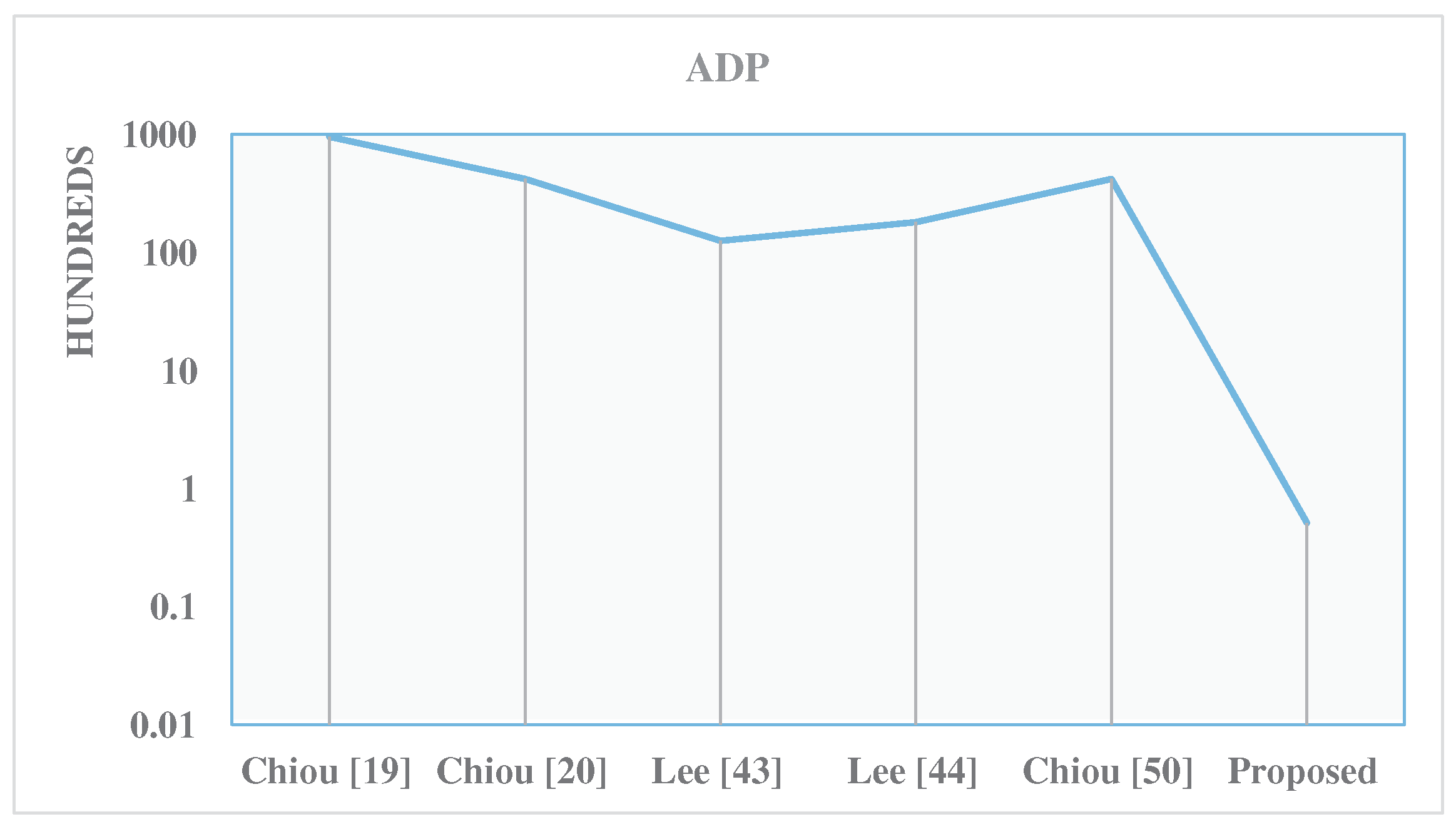
| Design | r | A [Kgates] | D [ns] | P [mW] | ADP | PDP | A Saving (%) | P Saving (%) | ADP Saving (%) | PDP Saving (%) |
|---|---|---|---|---|---|---|---|---|---|---|
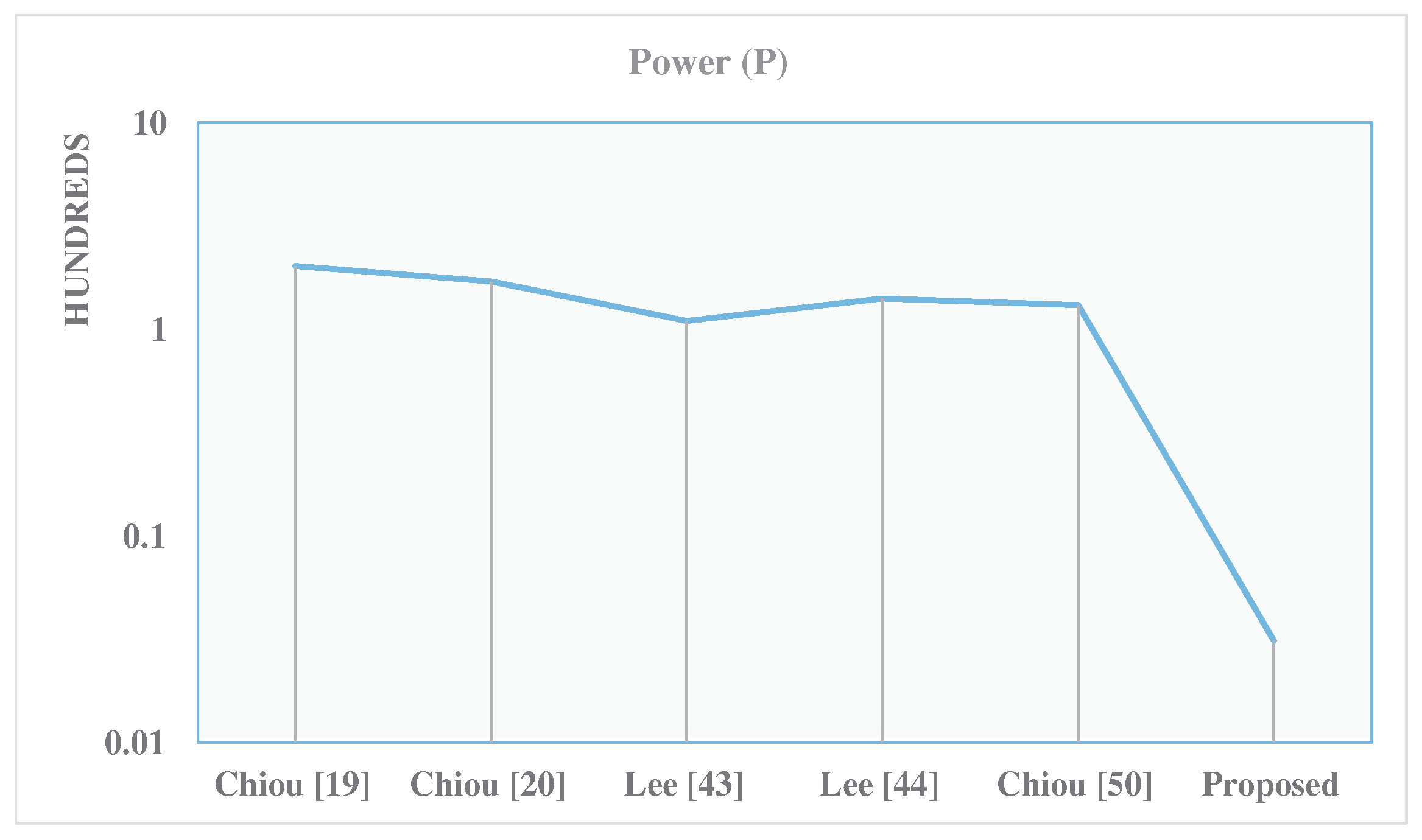
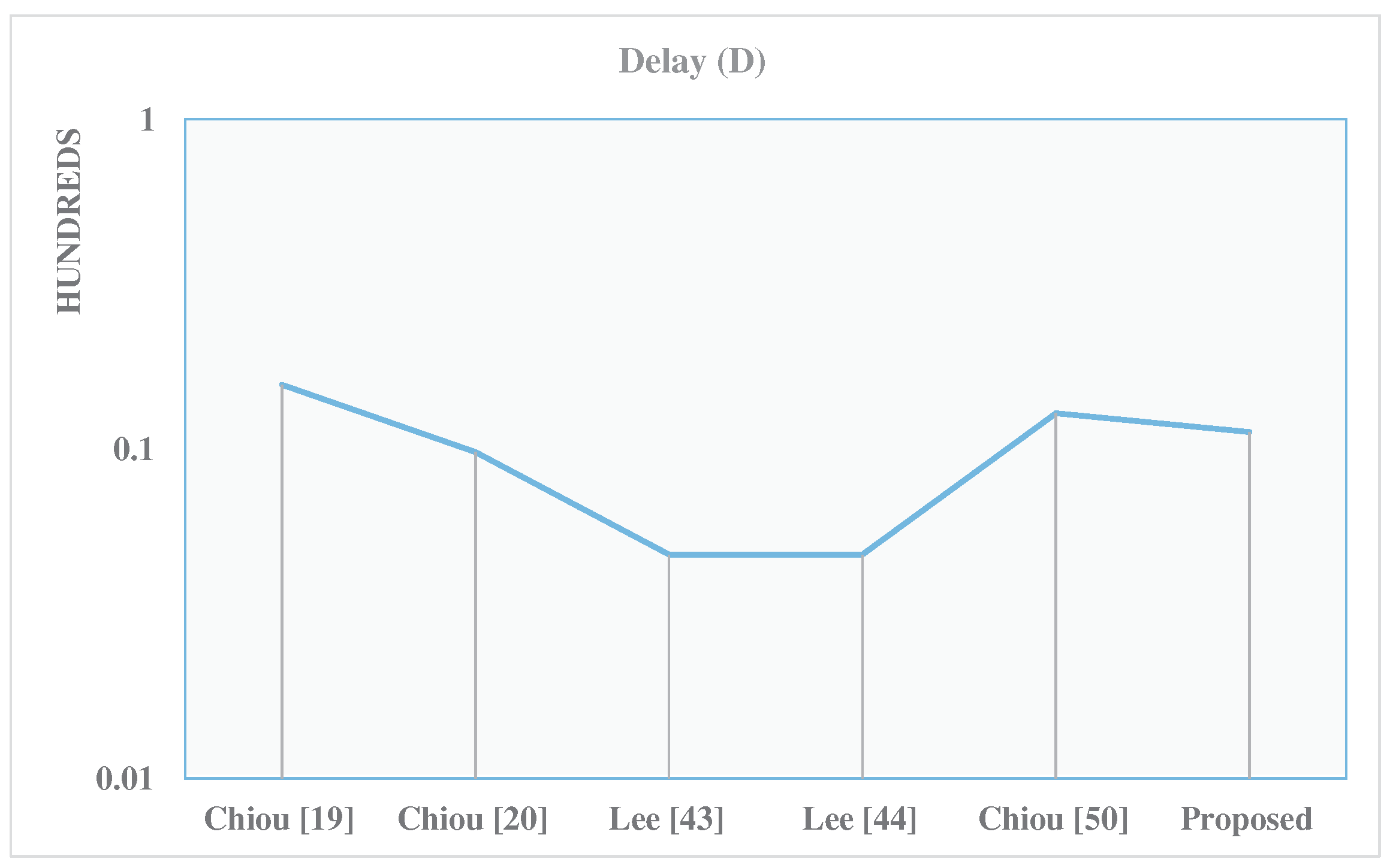
| Chiou [19] | 283 | 6083 | 15.6 | 202 | 95,117 | 3163 | 99.8 | 96.9 | 99.9 | 98.8 |
| Chiou [20] | 283 | 4276 | 9.8 | 170 | 41,720 | 1655 | 99.7 | 96.2 | 99.8 | 97.7 |
| Lee [43] | 283 | 2631 | 4.8 | 109.5 | 12,562 | 523 | 99.6 | 94.2 | 99.5 | 92.8 |
| Lee [44] | 283 | 3771.2 | 4.8 | 140 | 18,005 | 670 | 99.7 | 95.5 | 99.6 | 94.3 |
| Chiou [50] | 283 | 3274 | 12.8 | 131 | 41,904 | 1671 | 99.7 | 95.1 | 99.8 | 97.7 |
| Proposed | 283 | 4.5 | 11.2 | 3 | 51 | 34 | - | - | - |
Disclaimer/Publisher’s Note: The statements, opinions and data contained in all publications are solely those of the individual author(s) and contributor(s) and not of MDPI and/or the editor(s). MDPI and/or the editor(s) disclaim responsibility for any injury to people or property resulting from any ideas, methods, instructions or products referred to in the content. |
© 2025 by the authors. Licensee MDPI, Basel, Switzerland. This article is an open access article distributed under the terms and conditions of the Creative Commons Attribution (CC BY) license (https://creativecommons.org/licenses/by/4.0/).
Share and Cite
Ibrahim, A.; Gebali, F. Enhancing Security and Efficiency in IoT Assistive Technologies: A Novel Hybrid Systolic Array Multiplier for Cryptographic Algorithms. Appl. Sci. 2025, 15, 2660. https://doi.org/10.3390/app15052660
Ibrahim A, Gebali F. Enhancing Security and Efficiency in IoT Assistive Technologies: A Novel Hybrid Systolic Array Multiplier for Cryptographic Algorithms. Applied Sciences. 2025; 15(5):2660. https://doi.org/10.3390/app15052660
Chicago/Turabian StyleIbrahim, Atef, and Fayez Gebali. 2025. "Enhancing Security and Efficiency in IoT Assistive Technologies: A Novel Hybrid Systolic Array Multiplier for Cryptographic Algorithms" Applied Sciences 15, no. 5: 2660. https://doi.org/10.3390/app15052660
APA StyleIbrahim, A., & Gebali, F. (2025). Enhancing Security and Efficiency in IoT Assistive Technologies: A Novel Hybrid Systolic Array Multiplier for Cryptographic Algorithms. Applied Sciences, 15(5), 2660. https://doi.org/10.3390/app15052660